
1
White Electronic Designs Corporation (508) 366-5151 www.whiteedc.com
Sept. 2002 Rev. 3A
ECO #15528
EDI7F331MC
1Mx32 and 2x1Mx32 Densities
Based on AMD - AM29F080 Flash Device
Fast Read Access Time - 80ns
5- Volt-Only Reprogramming
Sector Erase Architecture
Uniform sectors of 64 Kbytes each
Any combination of sectors can be erased
Also supports full chip erase
Sector Protection
Hardware method that disables any combination of sectors
from write or erase operations
Embedded Erase Algorithms
Automatically preprograms and erases the chip or any
combination of sectors
Embedded Program Algorithms
Automatically programs and verifies data at specified
address
Data Polling and Toggle Bit feature for detection of program or
erase cycle completion
Low Power Dissipation
60mA per Device Active Current
10µA per Device CMOS Standby Current
Typical Endurance >100,000 Cycles
Single 5 Volt ±10% Supply
CMOS and TTL Compatible Inputs and Outputs
Commercial and Industrial Temperature Range
Package
80 Pin SIMM (JEDEC)
The EDI7F331MC and EDI7F2331MC are organized as one and
two banks of 1Mx32 respectively. The modules are based on
AMDs AM29F080 - 1Mx8 Flash device in TSOP packages which
are mounted on an FR4 substrate.
Both modules offer access times between 80 and 150ns allowing
for operation of high-speed microprocessors without wait states.
EDI7F331MC-BNC: 1Mx32 80 PIN SIMM
EDI7F2331MC-BNC: 2x1Mx32 80 PIN SIMM
1Mx32 FLASH MODULE
FEATURES
FIG. 1
BLOCK DIAGRAMS
A0-A19
G\
DQ0-DQ7
DQ8-DQ15
DQ16-DQ23
DQ24-DQ31
1Mx8
1Mx8
1Mx8
1Mx8
1Mx8
1Mx8
1Mx8
1Mx8
E1\
E0\
W0\
W1\
W2\
W3\
A0-A19
G\
DQ0-DQ7
DQ8-DQ15
DQ16-DQ23
DQ24-DQ31
1Mx8
1Mx8
1Mx8
1Mx8
E0\
W0\
W1\
W2\
W3\
DESCRIPTION
3
White Electronic Designs Corporation (508) 366-5151 www.whiteedc.com
Sept. 2002 Rev. 3A
ECO #15528
EDI7F331MC
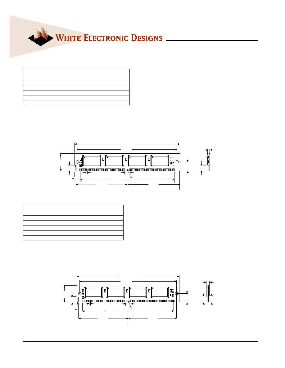
Pin Configurations and Block Diagram
Note: To order an Industrial grade product substitute the letter C in the Suffix with
the letter I.
ORDERING INFORMATION
PACKAGE NO. 346: 80 PIN SIMM (JEDEC)
PACKAGE NO. 361: 80 PIN SIMM (JEDEC)
J1
J3
153
0.062 R
0.062 R
0.850
MAX.
MIN.
4.655 MAX.
4.384
0.250
2.245
2.192
0.400
4.150
0.050 TYP.
0.250
0.120
MAX.
0.125
R3
R1
J1
J3
153
P1
0.850
MAX.
4.150
0.050 TYP.
0.250
J2-1
J2-2
J2-3
0.062 R
0.062 R
MAX.
MIN.
0.225
MIN.
4.655 MAX.
4.384
0.250
2.245
2.192
0.400
0.170
0.125
R3
ORDERING INFORMATION
Note: To order an Industrial grade product substitute the letter C in the Suffix with
the letter I.
Part Number
Speed
Package
(ns)
EDI7F331MC80BNC
80
346
EDI7F331MC90BNC
90
346
EDI7F331MC100BNC
100
346
EDI7F331MC120BNC
120
346
EDI7F331MC150BNC
150
346
Part Number
Speed
Package
(ns)
EDI7F2331MC80BNC
80
361
EDI7F2331MC90BNC
90
361
EDI7F2331MC100BNC
100
361
EDI7F2331MC120BNC
120
361
EDI7F2331MC150BNC
150
361
ALL DIMENSIONS ARE IN INCHES
DATASHEET APPROVALS
ECO#
EDI PART NO.
NEW REV
DATE
APPROVAL:
INITIAL
DATE
CORRECTION ON PAGES
JUAN GUZMAN
MUKESH TRIVEDI
PAUL MARIEN
LARRY WINROTH
DAVE KELLY
MARK DOWNEY
DAVE HARRISON
TONY LEE
BOB KHEDERIAN
LUIS ESTELLA
YES
NO
LINE
:________
WILL THIS DATASHEET GO ON THE WEB?
FAMILY:
____________
PROD.TYPE:
________
ORG:___________
IS THIS A NEW DATASHEET?
DENSITY:________
SPEED:__________
WILL THIS DATASHEET REPLACE AN EXISTING
PKG:____________
DATASHEET THAT'S ALREADY ON THE WEB?
VOLTAGE:________
IF YES, WHAT DATASHEET IS IT REPLACING?
WHAT SECTION SHOULD THIS DATASHEET BE
PLACED IN ON THE WEB?
AFTER REVIEWING OR MAKING CORRECTIONS ON THE DATASHEET (S)
PLEASE SIGN-OFF ON THIS SHEET AND ,MAKE YOUR CORRECTIONS ≠ON
THE ORIGINAL COPY(S).
AFTER REVIEWING THE DATA SHEET, TEST ENGINEERING WILL COMPLETE THE SECTION BELOW.
TEST PROGRAM CHANGE REQUIRED:
YES:_________NO____________DATE:___________
TEST ENGINEER SIGNATURE___________________
IF YES, DO NOT RELEASE DATA SHEET UNTIL TEST PROGRAM CHANGE IS COMPLETED.
TEST PROGRAM CHANGE COMPLETION DATE:__________
TEST PROGRAM NAME AND REVISION_________________
TEST ENGINEER SIGNATURE__________________________
FO-00342R1.DOC
ECO# 14942
SHEET 1 OF
1
9/25/02
9/26/02
9/27/02
L.K.
M.A.
EDI7F331MC
15528
3A
9/23/02
