EDI7F4331MC
1
White Electronic Designs Corporation ∑ (602) 437-1520 ∑ www.wedc.com
White Electronic Designs
Sept. 2002 Rev. 1A
White Electronic Designs Corp. reserves the right to change products or specifications without notice.
The EDI7F4331MC is organized as four banks of 1Mx32.
The module is based on AMDs AM29F080 - 1Mx8 Flash
device in TSOP packages which are mounted on an FR4
substrate.
The module offers access times between 80 and 150ns
allowing for operation of high-speed microprocessors
without wait states.
*This product is subject to change without notice.
n
4x1Mx32
n
Based on AMD - AM29F080 Flash Device
n
Fast Read Access Time - 80ns
n
5V Only Reprogramming
n
Sector Erase Architecture
n
Uniform sectors of 64 Kbytes each
n
Any combination of sectors can be erased
n
Also supports full chip erase
n
Sector Protection
n
Hardware method that disables any
combination of sectors from write or erase
operations
n
Embedded Erase Algorithms
n
Automatically pre-programs and erases the
chip or any combination of sectors
n
Embedded Program Algorithms
n
Automatically programs and verifies data at
specified address
n
Data Polling and Toggle Bit feature for detection of
program or erase cycle completion
n
Low Power Dissipation
n
60mA per Device Active Current
n
10µA per Device CMOS Standby Current
n
Typical Endurance >100,000 Cycles
n
Single 5V ±10% Supply
n
CMOS and TTL Compatible Inputs and Outputs
n
Commercial and Industrial Temperature Range
n
Package
n
80 Pin SIMM (JEDEC)
4x1Mx32 FLASH MODULE
DESCRIPTION
FEATURES

EDI7F4331MC
4
White Electronic Designs Corporation ∑ (602) 437-1520 ∑ www.wedc.com
White Electronic Designs
Sept. 2002 Rev. 1A
White Electronic Designs Corp. reserves the right to change products or specifications without notice.
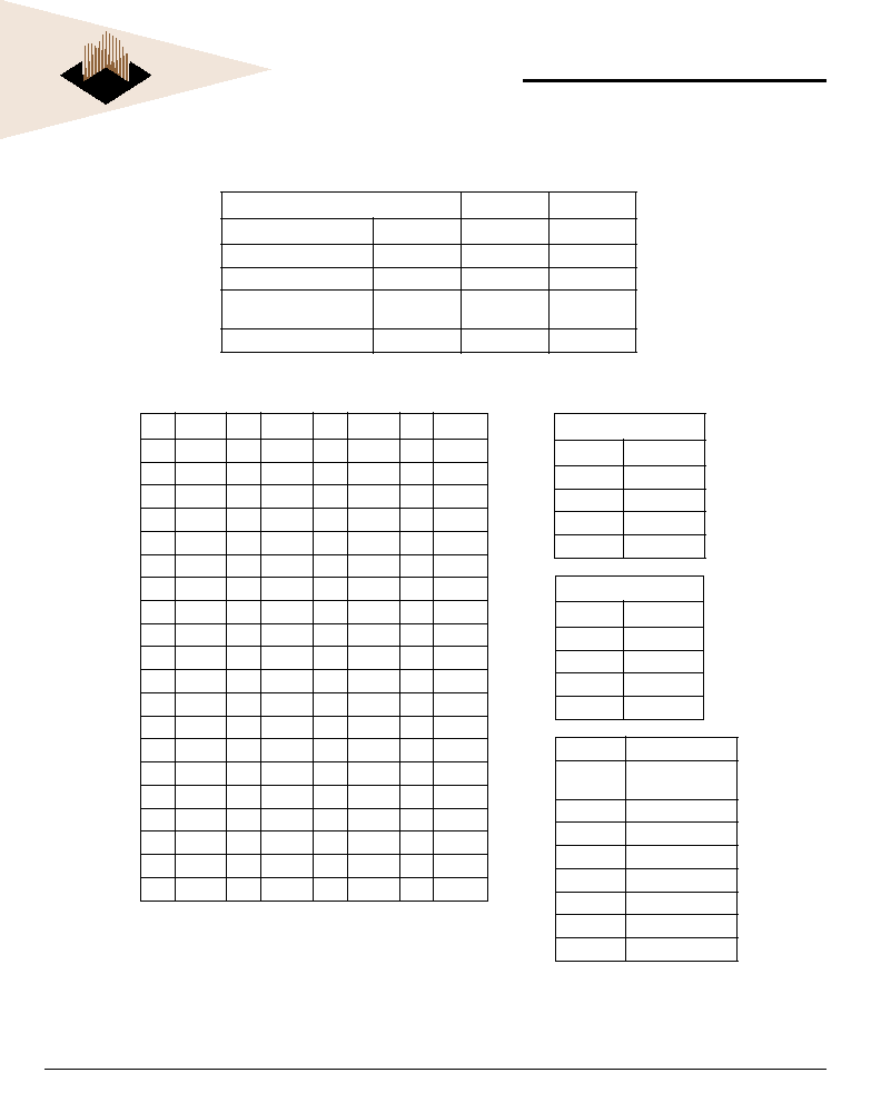
ORDERING INFORMATION
PACKAGE NO. 394: 80 PIN SIMM (JEDEC)
Note: To order an Industrial grade product substitute the letter C in the Suffix
with the letter I.
Part Number
Speed
(ns)
Package
EDI7F4331MC80BNC
80
394
EDI7F4331MC90BNC
90
394
EDI7F4331MC100BNC
100
394
EDI7F4331MC120BNC
120
394
EDI7F4331MC150BNC
150
394
ALL DIMENSIONS ARE IN INCHES