1
White Electronic Designs Corporation (508) 366-5151 www.whiteedc.com
White Electronic Designs
EDI8F82049C
FEATURES
2 M x 8 bit CMOS Static
Random Access Memory
Access Times 70 thru 100ns
Data Retention Function (EDI8F82049LP )
TTL Compatible Inputs and Outputs
Fully Static, No Clocks
High Density Packaging
36 Pin SIP, No. 136
Single +5V (±10%) Supply Operation
DESCRIPTION
The EDI8F82049C is a 16Mb CMOS Static RAM based on four
512K x 8 Static RAMs mounted on a multi-layered epoxy laminate
(FR4) substrate.
A low power version with data retention (EDI8F82049LP) is also
available.
The EDI8F82049C is offered in a 36 pin single-in-line package
(SIP), which provides a cost effective solution to very high packing
density.
All inputs and outputs are TTL compatible and operate from a
single 5V supply.
Fully asynchronous, the EDI8F82049C requires no clocks or
refreshing for operation.
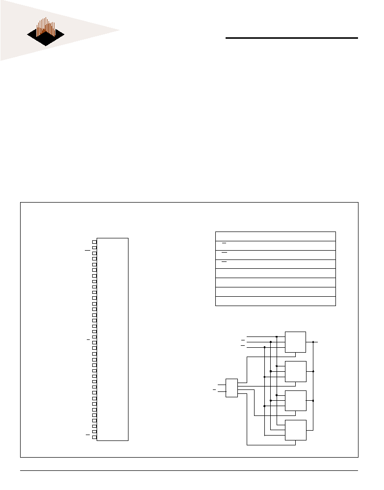
FIG. 1
PIN CONFIGURATION
PIN NAMES
2 Mb x 8 Static RAM CMOS, Module
BLOCK DIAGRAM
Aÿ-A20
Address Inputs
E
Chip Enable
W
Write Enable
G
Output Enable
DQÿ-DQ7
Common Data Input/Output
VCC
Power (+5V±10%)
VSS
Ground
NC
No Connection
DQ
0-7
512K x 8
512K x 8
512K x 8
512K x 8
A
0-18
W
G
A
19-20
E
DEC
1
2
3
4
5
6
7
8
9
10
11
12
13
14
15
16
17
18
19
20
21
22
23
24
25
26
27
28
29
30
31
32
33
34
35
36
A19
VCC
W
DQ2
DQ3
DQ0
A1
A2
A3
A4
VSS
DQ5
A10
A11
A5
A13
A14
A20
E
A15
A16
A12
A18
A6
DQ1
VSS
A0
A7
A8
A9
DQ7
DQ4
DQ6
A17
VCC
G
PIN OUT
July 2002 Rev.1
ECO # 15335
2
White Electronic Designs Corporation Westborough MA (508) 366-5151
White Electronic Designs
EDI8F82049C
ABSOLUTE MAXIMUM RATINGS*
RECOMMENDED DC OPERATING CONDITIONS
DC ELECTRICAL CHARACTERISTICS
CAPACITANCE
(F=1.0MHZ, VIN=VCC OR VSS)
AC TEST CONDITIONS
* Stress greater than those listed under "Absolute Maximum Ratings" may cause
permanent damage to the device. This is a stress rating only and functional operation
of the device at these or any other conditions greater than those indicated in the
operational sections of this specification is not implied. Exposure to absolute maximum
rating conditions for extended periods may affect reliability.
TRUTH TABLE
Parameter
Sym
Min
Typ
Max
Units
Supply Voltage
VCC
4.5
5.0
5.5
V
Supply Voltage
VSS
0
0
0
V
Input High Voltage
VIH
2.2
--
6.0
V
Input Low Voltage
VIL
-0.3
--
0.8
V
NOTE: For TEHQZ,TGHQZ and TWLQZ, CL = 5pF
Input Pulse Levels
VSS to 3.0V
Input Rise and Fall Times
5ns
Input and Output Timing Levels
1.5V
Output Load
TTL, CL =100pF
Parameter
Sym
Conditions
Min
Typ*
Max
Units
Operating Power
ICC1
W, E = VIL, II/O = 0mA,
--
105
mA
Supply Current
Min Cycle
Standby (TTL) Power
ICC2
E ≥ VIH, VIN £ VIL
--
10
mA
Supply Current
VIN ≥ VIH
Full Standby Power
ICC3
E ≥ VCC-0.2V
C
--
15
mA
Supply Current (CMOS)
VIN ≥ VCC-0.2V or
LP
--
1
mA
VIN £ 0.2V
Input Leakage Current
ILI
VIN = 0V to VCC
--
--
±20
µA
Output Leakage Current
ILO
V I/O = 0V to VCC
--
--
±20
µA
Output High Voltage
VOH
IOH =-1.0mA
2.4
--
--
V
Output Low Voltage
VOL
IOL = 2.1mA
--
--
0.4
V
*Typical: TA = 25∞C, VCC = 5.0V
G
E
W
Mode
Output
Power
X
H
X
Standby
High Z
ICC2, ICC3
H
L
H
Output Deselect
High Z
ICC1
L
L
H
Read
DOUT
ICC1
X
L
L
Write
DIN
ICC1
Parameter
Sym
Max
Unit
Address Lines
CI
32
pF
Data Lines
CD/Q
40
pF
Chip Enable and A17-A20 Lines
CC
32
pF
These parameters are sampled, not 100% tested.
Voltage on any pin relative to VSS
-0.5V to 7.0V
Operating Temperature TA (Ambient)
Commercial
0∞C to +70∞C
Industrial
-40∞C to +85∞C
Storage Temperature
-55∞C to +125∞C
Power Dissipation
1 Watt
Output Current.
20 mA
3
White Electronic Designs Corporation (508) 366-5151 www.whiteedc.com
White Electronic Designs
EDI8F82049C
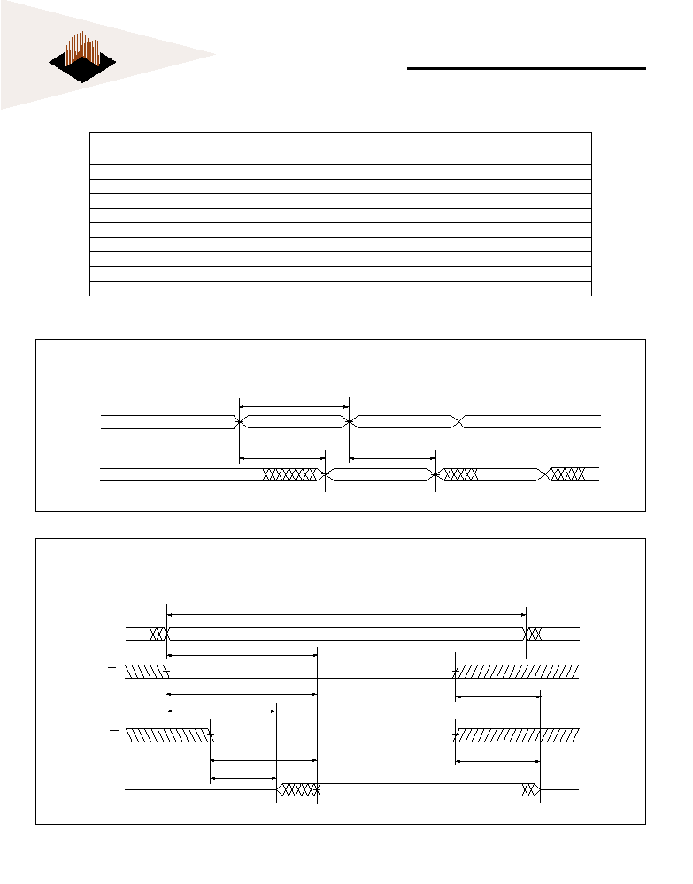
AC CHARACTERISTICS READ CYCLE
FIG. 2
READ CYCLE 1 - W HIGH, G, E LOW
FIG. 3
READ CYCLE 2 - W HIGH
Symbol
70ns
85ns
100ns
Parameter
JEDEC
Alt.
Min Max
Min
Max Min
Max Units
Read Cycle Time
TAVAV
TRC
70
85
100
ns
Address Access Time
TAVQV
TAA
70
85
100
ns
Chip Enable Access Time
TELQVTACS
70
85
100
ns
Chip Enable to Output in Low Z (1)
TELQX TCLZ
5
5
5
ns
Chip Disable to Output in High Z (1)
TEHQZ TCHZ
30
35
40
ns
Output Hold from Address Change
TAVQX TOH
3
3
3
ns
Output Enable to Output Valid
TGLQV TOE
40
45
50
ns
Output Enable to Output in Low Z (1)
TGLQX TOLZ
0
0
0
ns
Output Disable to Output in High Z (1)
TGHQZ TOHZ
30
35
40
ns
Note: Parameter guaranteed, but not tested.
ADDRESS 1
ADDRESS 2
TAVAV
DATA 1
DATA 2
TAVQV
TAVQX
A
Q
E
G
Q
A
TAVQV
TELQV
TELQX
TAVAV
TGLQX
TGLQV
TGHQZ
TEHQZ
4
White Electronic Designs Corporation Westborough MA (508) 366-5151
White Electronic Designs
EDI8F82049C
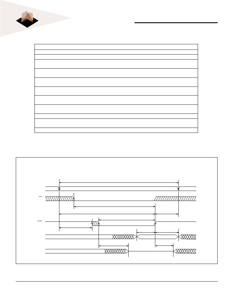
FIG. 4
WRITE CYCLE 1 - W CONTROLLED
AC CHARACTERISTICS WRITE CYCLE
Note: Parameter guaranteed, but not tested.
Write Cycle
Symbol
70ns
85ns
100ns
Parameter
JEDEC
Alt.
Min Max
Min
Max Min
Max Units
Write Cycle Time
TAVAV
TWC
70
85
100
ns
Chip Enable to End of Write
TELWH TCW
65
70
80
ns
TELEH TCW
65
70
80
ns
Address Setup Time
TAVWL
TAS
0
0
0
ns
TAVEL
TAS
0
0
0
ns
Address Valid to End of Write
TAVWH TAW
65
70
80
ns
TAVEH TAW
65
70
80
ns
Write Pulse Width
TWLWH TWP
65
70
80
ns
TWLEH TWP
65
70
80
ns
Write Recovery Time
TWHAX TWR
0
0
0
ns
TEHAX TWR
0
0
0
ns
Data Hold Time
TWHDX TDH
0
0
0
ns
TEHDX TDH
0
0
0
ns
Write to Output in High Z (1)
TWLQZ TWHZ
0
30
0
35
0
40
ns
Data to Write Time
TDV WH TDW
30
35
40
ns
TDV EH TDW
30
35
40
ns
Output Active from End of Write (1)
TWHQX TWLZ
5
5
5
ns
E
A
TAVAV
TELWH
TAVWH
TWLWH
TAVWL
TWHAX
W
HIGH Z
DATA VALID
TWLQZ
TWHQX
TDVWH
TWHDX
Q
D
5
White Electronic Designs Corporation (508) 366-5151 www.whiteedc.com
White Electronic Designs
EDI8F82049C
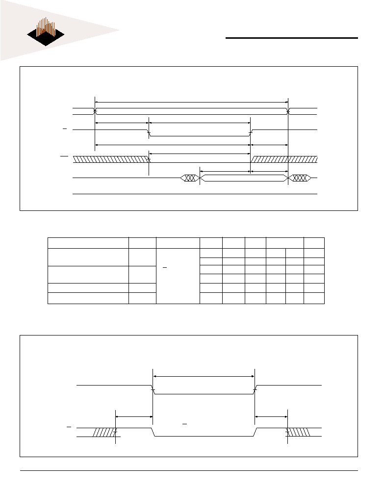
FIG. 5
WRITE CYCLE 2 - E CONTROLLED
DATA RETENTION CHARACTERISTICS
FIG. 6
DATA RETENTION - E CONTROLLED
Characteristic
Sym
Test Conditions
VDD
Min
Typ
Max
Unit
70∞C
85∞C
Data Retention Voltage
VDD
2
--
--
--
V
Data Retention Quiescent Current
ICCDR
E ≥ VDD - 0.2V
2V
--
150
200
µA
VIN ≥ VDD - 0.2V
3V
250
400
µA
Chip Disable to Data Retention Time(1) TCDR
or VIN £ 0.2V0
--
--
--
ns
Operation Recovery Time (1)
TR
TAVAV*
--
--
--
ns
Note: Parameter guaranteed, but not tested.
* Read Cycle Time
LP Version Only
A
TAVEL
HIGH Z
TAVAV
TELEH
E
TAVEH
TEHAX
W
TWLEH
TEHDX
TDVEH
Q
DATA VALID
D
VCC
E
TCDR
TR
Data Retention Mode
E
VDD -0.2V
4.5V
VDD
4.5V

6
White Electronic Designs Corporation Westborough MA (508) 366-5151
White Electronic Designs
EDI8F82049C
PACKAGE NO. XXX
36 PIN SINGLE-IN-LINE PACKAGE
ORDERING INFORMATION
Standard Power
Low Power
Speed
Package
with Data Retention
(ns)
No.
EDI8F82049C70BSC
EDI8F82049LP70BSC
70
xxx
EDI8F82049C85BSC
EDI8F82049LP85BSC
85
xxx
EDI8F82049C100BSC
EDI8F82049LP100BSC
100
xxx
Note: To order an Industrial grade product substitute the letter C in the Suffix with the letter I,
(e.g., EDI8F82049C70BSC becomes EDI8F82049C70BSI).
3.805 MAX
3.500 ± 0.003
0.100 (35 plcs)
0.855
MAX
0.144
MAX
ALL DIMENSIONS ARE IN INCHES