1
White Electronic Designs Corporation ∑ (508) 366-5151 ∑ www.whiteedc.com
EDI8L21665V
February 1999 Rev. 0
ECO #
DESCRIPTION
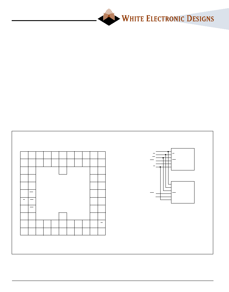
The EDI8L21665VxxBC is a 3.3V, 2x64Kx16 SRAM constructed
with two 64Kx16 die mounted on a multi-layer laminate substrate.
The device is packaged in a 74 lead, 15mm by 15mm, BGA.
Operating with a 3.3V power supply and with access times as fast
as 10ns, the device allows the user to develop a fast external
memory for Texas Instuments' TMS320C5x DSP.
The device consists of two separate banks of 64Kx16 of memory.
Each bank has a separate Chip Enable pin and higher order
address select pin. Bank `A' is controlled using CE
1
\ and A
15A
.
Bank `B' is controlled using CE
2
\ and A
15B
. The two banks have
common I/Os (DQ
0-15
) and control lines (WE\, E\ and G\). E\
connects to the mstrb\ pin of the C54x DSPs and is required for
write and read timing control.
FEATURES
s Access Times of 10, 12 and 15ns
s DSP Memory Solution
∑ Texas Instruments TMS320C5x
s Packaging:
∑ 74 pin BGA, JEDEC MO-151
s 3.3V Operating Supply Voltage
s Single Write Control and Output Enable Lines
s One Chip Enable Line per Memory Bank
s 50% Space Savings vs. Monolithic TSOPs
s Upgrade Path Available in Same Footprint
s Multiple V
CC
and V
SS
Pins
s Reduced Inductance and Capacitance
BLOCK DIAGRAM
PIN CONFIGURATION
A
0
-
14
G
W
CE
1
A
15A
E
G
CE
A
15
CE
A
15
CE
2
A
15A
64K X 16
SSRAM
64K X 16
SSRAM
U1
U2
1
2
3
4
5
6
7
8
9
10
11
A
Vss
Vcc
Vcc DQ
15
DQ
14
Vcc DQ
13
DQ
11
DQ
9
DQ
8
NC
A
B
Vss
Vcc
Vcc Vss
Vss
Vcc DQ
12
DQ
10
DQ
4
Vcc Vcc
B
C
Vss
Vss
Vcc
Vss Vcc
C
D
Vss
Vss
Vss Vcc
D
E
Vss
Vss
Vss Vcc
E
F A
15A
CE
1
DQ
3
DQ
7
F
G
E
W
DQ
5
DQ
0
G
H
Vss
CE
2
DQ
6
DQ
1
H
I
Vss
A
14
Vcc
DQ
2
NC
I
J
Vss
A
12
Vcc A
10
A
8
Vss
A
6
A
4
A
2
A
0
G
J
K A
15B
A
13
Vcc A
11
A
9
Vss
A
7
V
SS
A
5
A
3
A
1
K
1
2
3
4
5
6
7
8
9
10
11
2x64Kx16 SRAM, DSP Memory Solution
2
White Electronic Designs Corporation ∑ (508) 366-5151 ∑ www.whiteedc.com
EDI8L21665V
RECOMMENDED OPERATING CONDITIONS
Description
Symbol
Min
Max
Unit
Input High Voltage
V
IH
2.2
Vcc+0.5
V
Input Low Voltage
V
IL
-0.3
0.8
V
Supply Voltage
Vcc
3.0
3.6
V
CAPACITANCE
(f = 1MHz, V
IN
= V
CC
or V
SS
)
Voltage on Vcc Supply Relative to Vss
-0.5V to 4.6V
V
IN
-0.5V to Vcc+0.5V
Storage Temperature
-55
∞
C to +125
∞
C
Junction Temperature
+125
∞
C
Power Dissipation
3 Watts
Short Circuit Output Current (per I/O)
50 mA
* Stress greater than those listed under "Absolute Maximum Ratings" may cause perma-
nent damage to the device. This is a stress rating only and functional operation of the
device at these or any other conditions greater than those indicated in the operational
sections of this specification is not implied. Exposure to absolute maximum rating condi-
tions for extended periods may affect reliability.
Parameter
Symbol
Max
Unit
Address Lines
CA
8
pF
Data Lines
CD/Q
17
pF
Control Lines
CC
15
pF
PIN DESCRIPTIONS
Pin
Symbol
Type
Description
A
0-14
Input
Addresses
A
15A
Input
Addresses: A
15
on Bank `A' of memory
A
15B
Input
Addresses: A
15
on Bank `B' of memory
W
Input
Write Enable: This active LOW input allows a full 16-bit WRITE to occur.
CE
1
Input
Chip Enable: This active LOW input is used to enable the `A' Bank of the device.
CE
2
Input
Chip Enable: This active LOW input is used to enable the `B' Bank of the device.
G
Input
Output Enable: This active LOW asynchronous input enables the data output drivers.
Various
DQ
0-15
Input/Output
Data Inputs/Outputs
Various
Vcc
Supply
Core power supply: +3.3V -5%/+10%
Various
Vss
Ground
Ground
E
Input
Enable, This active LOW input controls Write and Read Timing
DC ELECTRICAL CHARACTERISTICS
(f = 1MHz, V
IN
= V
CC
or Vss)
Parameter
Symbol
Conditions
Min
Max
Units
Device Selected; all inputs
V
IL
or
V
IH
;
-10ns
380
mA
Power Supply Current: Operating
ICC1
cycle time
t
KC
MIN;
-12ns
360
V
CC
= MAX; outputs open
-15ns
260
Device deselected; V
CC
= MAX;
CMOS Standby
ISB2
all inputs
V
SS
+0.2 or
V
CC
-0.2; all inputs static;
60
mA
CLK frequency = 0
TTL Standby
ISB3
Device deselected; all inputs
V
IL
or
V
IH
;
120
mA
all inputs static; V
CC
= MAX; CLK frequency = 0
Input Leakage Current
ILI
0V
V
IN
V
CC
-5
5
µ
A
Output Leakage Current
ILO
Output(s) disabled, 0V
V
OUT
V
CC
-5
5
µ
A
Output High Voltage
VOH
IOH = -4.0mA
2.4
V
Output Low Voltage
VOL
IOL = 8.0mA
0.4
V
ABSOLUTE MAXIMUM RATINGS*

3
White Electronic Designs Corporation ∑ (508) 366-5151 ∑ www.whiteedc.com
EDI8L21665V
AC TEST CIRCUIT
AC TEST CONDITIONS
50
Vt = 1.5V
Output
Z0 = 50
Z0 = 50
Parameter
I/O
Unit
Input Pulse Levels
V
SS
to 3.0
V
Input Rise and Fall Times (max)
1.5
ns
Input and Output Timing Levels
1.5
V
Output Load
See figure, at left
AC Output Load Equivalent
1.25V
AC ELECTRICAL CHARACTERISTICS
Symbol
10ns
12ns
15ns
Read Cycle
Min
Max
Min
Max
Min
Max
Units
Read Cycle Time
t
AVAV
10
12
15
ns
Address Access Time
t
AVQV
10
12
15
ns
Chip Enable Access
t
ELQV
10
12
15
ns
Output Hold from Address Change
t
AVQX
3
4
4
ns
Chip Enable to Output in Low-Z
t
ELQX
3
4
4
ns
Chip Disable to Output in High-Z
t
EHQZ
5
6
7
ns
Output Enable access time
t
GLQV
5
6
7
ns
Output Enable to Output in Low-Z
t
GLQX
0
0
0
ns
Output Disable to Output in High-Z
t
GHQZ
5
6
7
ns
Write Cycle
Write Cycle Time
t
AVAV
10
12
15
ns
Chip Enable to End of Write
t
ELWH
8
8
9
ns
Address valid to End of Write, with G HIGH
t
AVGHWH
8
8
9
ns
Address Setup Time
t
AVWL
0
0
0
ns
Address Hold from End of Write
t
AVWH
8
8
10
ns
Write Pulse Width
t
WLWH
10
10
11
ns
Write Pulse Width, with G HIGH
t
WLGHWH
8
8
9
ns
Data Setup Time
t
DVWH
6
6
7
ns
Data Hold Time
t
WHDX
0
0
0
ns
Write Disable to Output in Low-Z
t
WHQX
3
4
5
ns
Write Enable to Output in High-Z
t
WLQZ
5
6
7
ns

4
White Electronic Designs Corporation ∑ (508) 366-5151 ∑ www.whiteedc.com
EDI8L21665V
READ CYCLE TIMING DIAGRAMS
A
Q
READ CYCLE 1 (W HIGH; G, E LOW)
t
AVQX
t
AVQV
t
AVAV
DATA 2
ADDRESS 1
ADDRESS 2
DATA 1
A
Q
READ CYCLE 2 (W HIGH)
t
AVQV
t
ELQV
t
GLQV
t
ELQX
t
GLQX
t
AVAV
t
EHQZ
t
GHQZ
G
E
WRITE CYCLE TIMING DIAGRAM
A
D
WRITE CYCLE 2, E CONTROLLED
t
AVEH
t
ELEH
t
EHAX
t
DVEH
t
EHDX
t
AVAV
DATA VALID
HIGH Z
W
E
Q
t
AVEL
NOTES: All Writes are E controlled when connected to the TMS320C54X. E is connected to MSTRB and W is connected to R/W of the TMS320C54X.
5
White Electronic Designs Corporation ∑ (508) 366-5151 ∑ www.whiteedc.com
EDI8L21665V
EDI8L21665V
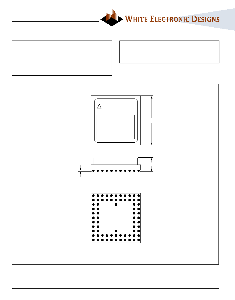
PACKAGE DESCRIPTION:
74 PIN BGA
PACKAGE NO. 428
THERMAL PACKAGE
PERFORMANCE:
J
A
= 28
∞
C/Watt (Natural Connection)
J
B
= 4
∞
C/Watt
Commercial Temperature Range (0
∞
C to +70
∞
C)
Part Number
Speed
Package
(ns)
No.
EDI8L21665V10BC
10
428
EDI8L21665V12BC
12
428
EDI8L21665V15BC
15
428
ORDERING INFORMATION
0.591 SQ.
0.125 MAX
0.029 MAX
ALL DIMENSIONS ARE IN INCHES
Industrial Temperature Range (-40
∞
C to +85
∞
C)
Part Number
Speed
Package
(ns)
No.
EDI8L21665V15BI
15
428