EDI9F37512C
512Kx37 SRAM Module
1
EDI9F37512C Rev. 3 4/98 ECO #9755
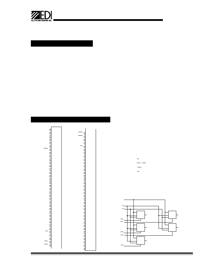
Aÿ-A18
Address Inputs
E
Chip Enables
W0-W3
Write Enable
AW
Parity Write Enable
G
Output Enable
DQÿ-DQ31
Common Data Input/Output
VCC
Power (+5V±10%)
VSS
Ground
PD0-PD1
Presence Detect
Features
512Kx37 bit CMOS Static
Random Access Memory
∑ Access Times: 45 and 55 ns
∑ Individual Byte Selects
∑ Fully Static, No Clocks
∑ TTL Compatible I/O
High Density Package
∑ 72 lead SIMM, No. 418
∑ Common Data Inputs and Outputs
Single +5V (±10%) Supply Operation
The EDI9F37512C is a high speed 20 megabit Static
RAM module organized as 512K words x 37 bits. This
module is constructed from five 512Kx8 Static RAMs in
TSOP packages on an epoxy laminate (FR4) board.
Four write selects (W0-W3) are used to independently
enable the four bytes. Reading and writing can be
executed on individual bytes or any combination of
multiple bytes through proper use of selects.
The EDI9F37512C is offered in a 72 lead SIMM which
allows 20 megabits of memory to be placed in less than
1.5 square inch or board space.
All inputs and outputs are TTL compatible and operate
from a single 5V supply. Fully asynchronous circuitry
requires no clocks or refreshing for operation and pro-
vides equal access and cycle times for ease of use.
The SIMM module contains two Presence Detect pins
which are used to identify module memory density in
applications where alternate modules can be inter-
changed.
Pin Configurations and Block Diagram
Pin Names
512Kx37 Static RAM
CMOS, High Speed Module
Electronic Designs Incorporated
∑ One Research Drive ∑ Westborough, MA 01581 USA ∑ 508-366-5151 ∑ FAX 508-836-4850 ∑
http://www.electronic-designs.com
32
10
11
12
13
14
15
16
17
18
19
20
21
22
23
24
25
26
27
28
29
30
31
33
34
35
36
DQ1
DQ3
DQ8
DQ9
DQ2
DQ10
DQ11
VCC
DQ4
DQ13
DQ5
DQ14
DQ6
DQ15
DQ7
VSS
AD3
AD4
AD1
AD2
VSS
AD0
DQ0
A1
A3
A5
A7
W0
AW
A0
A2
A4
DQ12
A6
W1
E
1
2
3
4
5
6
7
8
9
VSS
DQ24
DQ16
DQ25
DQ17
DQ26
DQ18
DQ27
DQ19
VCC
DQ20
DQ28
DQ21
DQ29
DQ22
VSS
DQ30
DQ23
DQ31
37
38
39
40
41
42
43
44
45
46
47
48
49
50
51
54
56
57
58
59
60
61
62
63
64
65
66
67
68
69
70
71
72
52
53
55
W3
W2
NC
PD1
PD0
A10
A11
A12
A13
A14
A15
A16
A18
A17
A8
A9
G
DQ0-DQ7
DQ8-DQ15
DQ16-DQ23
DQ24-DQ31
W0
W1
W2
W3
AW
AD0-AD4
A0-A18
G
E

2
EDI9F37512C Rev. 3 4/98 ECO #9755
EDI9F37512C
512Kx37 SRAM Module
AC Characteristics Read Cycle
Symbo
45ns
55ns
Parameter
JEDEC
Alt.
Min
Max
Min
Max
Units
Read Cycle Time
TAVAV
TRC
45
55
ns
Address Access Time
TAVQV
TAA
45
55
ns
Chip Enable Access
TELQV
TACS
45
55
ns
Chip Enable to Output in Low Z (1)
TELQX
TCLZ
3
3
ns
Chip Disable to Output in High Z (1)
TEHQZ
TCHZ
18
25
ns
Output Hold from Address Change
TAVQX
TOH
3
3
ns
Output Enable to Output Valid
TGLQV
TOE
15
25
ns
Output Enable to Output in Low Z (1)
TGLQX
TOLZ
0
0
ns
Output Disable to Output in High Z(1)
TGHQZ TOHZ
15
15
ns
Read Cycle 2 - W High
Read Cycle 1 - W High, G, E Low
Notes: 1. Parameter guaranteed, but not tested.
TGHQZ
TELQV
TELQX
E
G
Q
TEHQZ
A
TGLQV
TGLQX
TAVQV
TAVAV
TAVQV
TAVQX
DATA 2
A
Q
ADDRESS 1
ADDRESS 2
DATA 1

EDI9F37512C
512Kx37 SRAM Module
3
EDI9F37512C Rev. 3 4/98 ECO #9755
Notes: 1. Parameter guaranteed, but not tested.
Symbol
45ns
55ns
Parameter
JEDEC
Alt.
Min
Max
Min
Max
Units
Write Cycle Time
TAVAV
TWC
45
55
ns
Chip Enable to End of Write
TELWH
TCW
25
45
ns
TWLEH
TCW
25
45
ns
Address Setup Time
TAVWL
TAS
0
0
ns
TAVEL
TAS
0
0
ns
Address Valid to End of Write
TAVWH
TAW
25
45
ns
TAVEH
TAW
25
45
ns
Write Pulse Width
TWLWH
TWP
25
40
ns
TELEH
TWP
25
40
ns
Write Recovery Time
TWHAX
TWR
0
0
ns
TEHAX
TWR
0
0
ns
Data Hold Time
TWHDX
TDH
0
0
ns
TEHDX
TDH
0
0
ns
Write to Output in High Z (1)
TWLQZ
TWHZ
0
6
0
28
ns
Data to Write Time
TDVWH
TDW
20
30
ns
TDVEH
TDW
20
30
ns
Output Active from End of Write (1) TWHQX
TWLZ
3
3
ns
AC Characteristics Write Cycle
Write Cycle 2 - E Controlled
A
W
E
D
Q
TAVAV
TAVEL
TEHAX
TDVEH
TEHDX
TELEH
TAVEH
DATA VALID
HIGH Z
TWLEH
4
EDI9F37512C Rev. 3 4/98 ECO #9755
EDI9F37512C
512Kx37 SRAM Module
Electronic Designs Incorporated
∑ One Research Drive ∑ Westborough, MA 01581USA ∑ 508-366-5151 ∑ FAX 508-836-4850 ∑
http://www.electronic-designs.com
Electronic Designs Inc. reserves the right to change specifications without notice. CAGE No. 66301
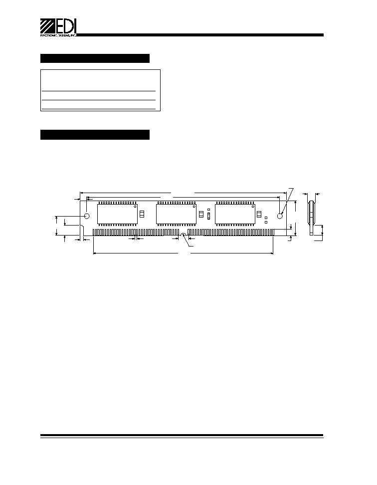
Package Description
Part Number
Speed
Package
(ns)
No.
EDI9F37512C45MMC
45
418
EDI9F37512C55MMC
55
418
Ordering Information
Package No. 418
72 Pin ZIP
.250
.050 TYP.
.125 DIA. TYP.
(2 PLCS.)
MAX.
3.984
4.255 MAX.
.130
REF.
.060 R.
3.750
.400
.250
.080
.220
MIN.
.720
MAX.
.300
.133 REF.
REF.
P1