August 2000 Rev. 3 - ECO #13134
1
PCMCIA Flash Memory Card
FVA Series
PC Card Products
Features
∑
Low cost Linear Flash Card
∑ Single 5 Volt Supply
∑Based on FlashFile
TM
Components
∑Fast Read Performance
- 100ns or 150ns Maximum Access Time
∑ x16 Data Interface
- Odd byte not accessible on Even byte
∑ High Performance Random Writes
- 10µs Typical Word Write Time
∑ Automated Write and Erase Algorithms
- Intel Command Set
∑ 50µA Typical Deep Power-Down
∑ 100,000 Erase Cycles per Block
∑ 64K word symmetrical Block Architecture
∑ PC Card Standard Type I Form Factor
The WEDC Value Series (FV) Flash memory cards
offers a low cost linear Flash solid state storage
solution for code and data storage, high performance
disk emulation, mobile PC and embedded
applications.
The WEDC Value series is based on Intel/Sharp Flash
memories. Cards are based on the 28F008SA (8Mb),
28F008S5 (8Mb) or 28F016S5 (16Mb) devices whose
device codes are A2H, A6H and AAH respectively.
Systems should be able to recognize all three codes.
The symmetrically blocked architecture and single 5V
operation provides a cost effective, high performance,
nonvolatile storage solution. The PC Card form factor
offers an industry standard pinout and mechanical
outline, allowing density upgrades without system
design changes.
The Value series is designed as a simple x16 linear
array of Flash devices. Two Flash devices in parallel
provide the lower and upper bytes for the 16 bit
access. The Value series does not provide access of
the ODD byte (D8 - D15) on the even byte data path
(D0 - D7).
WEDC's standard Value Series Flash Card is shipped
with no attribute memory or CIS (Card Information
Structure) information. An option for 2KB of attribute
memory with CIS information is available. The CIS
for the WEDC Value series may also be stored in
Block 0 (even bytes, D0 - D7 only) of the Flash
memory, this option is available by request only.
WEDC's standard cards are shipped with WEDC's
Logo. Cards are also available with blank housings
(no Logo). The blank housings are available in both a
recessed (for label) and flat housing. Please contact
WEDC sales representative for further information on
Custom artwork.
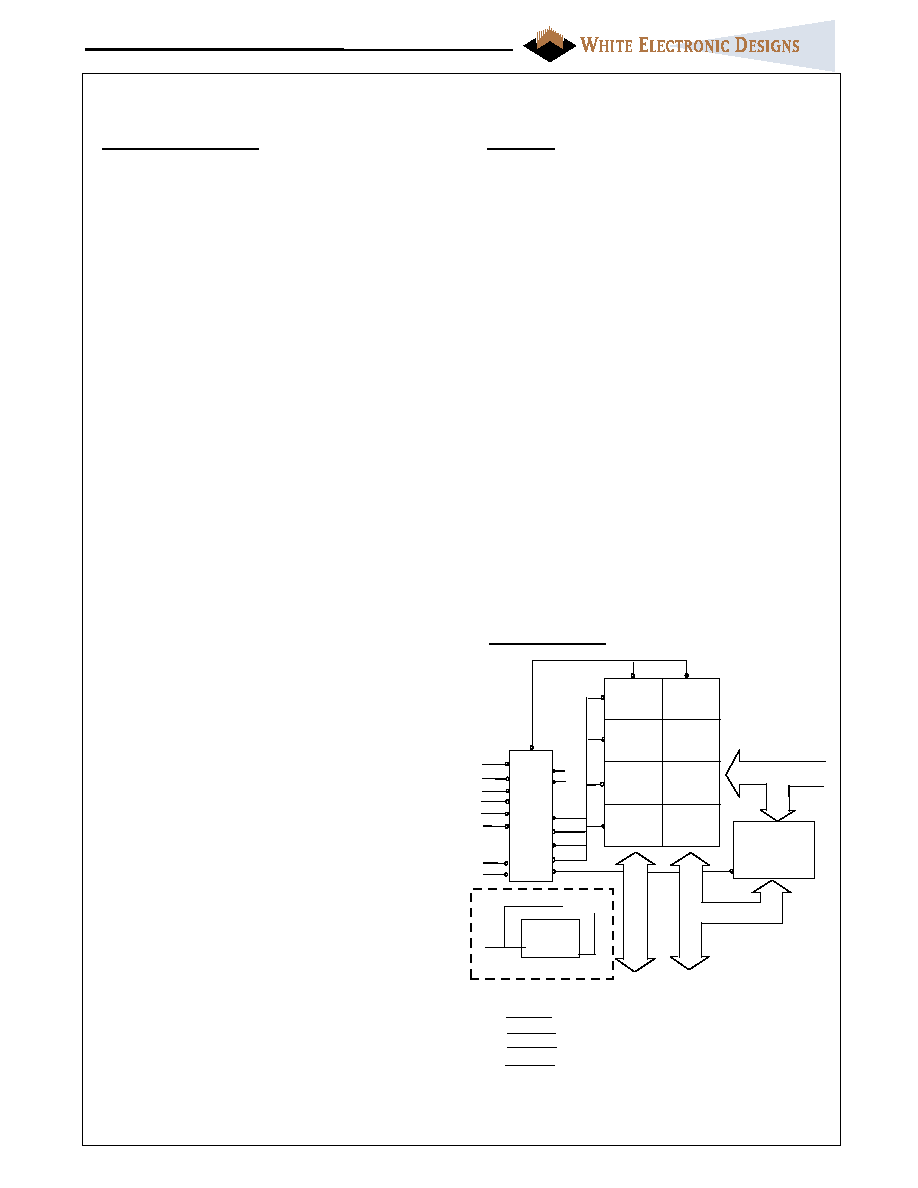
Value Series Flash Memory Card 2, 4, 8, 16 MEGABYTE (Intel/Sharp based )
Block Diagram
Note: VPP Generator only required for cards using
28F008SA devices configuration above for 8MB
card using 8Mbit components.
ADDRESS BUS A1-A20
DATA
D0-7
DATA
D8-15
ATTRIBUTE
MEMORY
28C16
CO
NTR
O
L
LO
G
I
C
/CE1
/CE2
/REG
/WE
/OE
A21
A22
Device 1
Device 3
Device 5
Device 7
Device 0
Device 2
Device 4
Device 6
Vpp
Generator
Vcc
Vcc
Vpp
Vpp1
Vpp2
VS1
VS2
open
/WR
/RD
RDY/BSY
Busy 0-7
General Description
August 2000 Rev. 3 - ECO #13134
2
PCMCIA Flash Memory Card
FVA Series
PC Card Products
Pin Signal name I/O
Function
Active
Pin Signal name I/O
Function
Active
1
GND
Ground
35
GND
Ground
2
DQ3
I/O
Data bit 3
36
CD1#
O
Card Detect 1
LOW
3
DQ4
I/O
Data bit 4
37
DQ11
I/O
Data bit 11
4
DQ5
I/O
Data bit 5
38
DQ12
I/O
Data bit 12
5
DQ6
I/O
Data bit 6
39
DQ13
I/O
Data bit 13
6
DQ7
I/O
Data bit 7
40
DQ14
I/O
Data bit 14
7
CE1#
I
Card enable 1
LOW
41
DQ15
I
Data bit 15
8
A10
I
Address bit 10
42
CE2#
I
Card Enable 2
LOW
9
OE#
I
Output enable
LOW
43
VS1
O
Voltage Sense 1
N.C.
10
A11
I
Address bit 11
44
RFU
Reserved
11
A9
I
Address bit 9
45
RFU
Reserved
12
A8
I
Address bit 8
46
A17
I
Address bit 17
13
A13
I
Address bit 13
47
A18
I
Address bit 18
14
A14
I
Address bit 14
48
A19
I
Address bit 19
15
WE#
I
Write Enable
LOW
49
A20
I
Address bit 20
2MB(2)
16 RDY/BSY# O
Ready/Busy
LOW
50
A21
I
Address bit 21
4MB(2)
17
Vcc
Supply Voltage
51
Vcc
Supply Voltage
18
Vpp1
Prog. Voltage
N.C.
52
Vpp2
Prog. Voltage
N.C.
19
A16
I
Address bit 16
53
A22
I
Address bit 22
8MB(2)
20
A15
I
Address bit 15
54
A23
I
Address bit 23
16MB(2)
21
A12
I
Address bit 12
55
A24
I
Address bit 24
N.C.
22
A7
I
Address bit 7
56
A25
I
Address bit 25
N.C.
23
A6
I
Address bit 6
57
VS2
O
Voltage Sense 2
N.C.
24
A5
I
Address bit 5
58
RST
I
Card Reset
HIGH
25
A4
I
Address bit 4
59
Wait#
O Extended Bus cycle LOW
26
A3
I
Address bit 3
60
RFU
Reserved
27
A2
I
Address bit 2
61
REG#
I
Attrib Mem Select
28
A1
I
Address bit 1
62
BVD2
O Bat. Volt. Detect 2
29
A0
I
Address bit 0
N.C.
63
BVD1
O Bat. Volt. Detect 1
30
DQ0
I/O
Data bit 0
64
DQ8
I/O
Data bit 8
31
DQ1
I/O
Data bit 1
65
DQ9
I/O
Data bit 9
32
DQ2
I/O
Data bit 2
66
DQ10
O
Data bit 10
33
WP
O
Write Potect
HIGH
67
CD2#
O
Card Detect 2
LOW
34
GND
Ground
68
GND
Ground
Pinout
Notes:
1. RDY/BSY signal is a full CMOS output, pull-up resistors are not required.
2. Shows density for which specified address bit is MSB. Higher order address bits are no
connects (ie 4MB A21 is MSB A22 - A25 are NC).
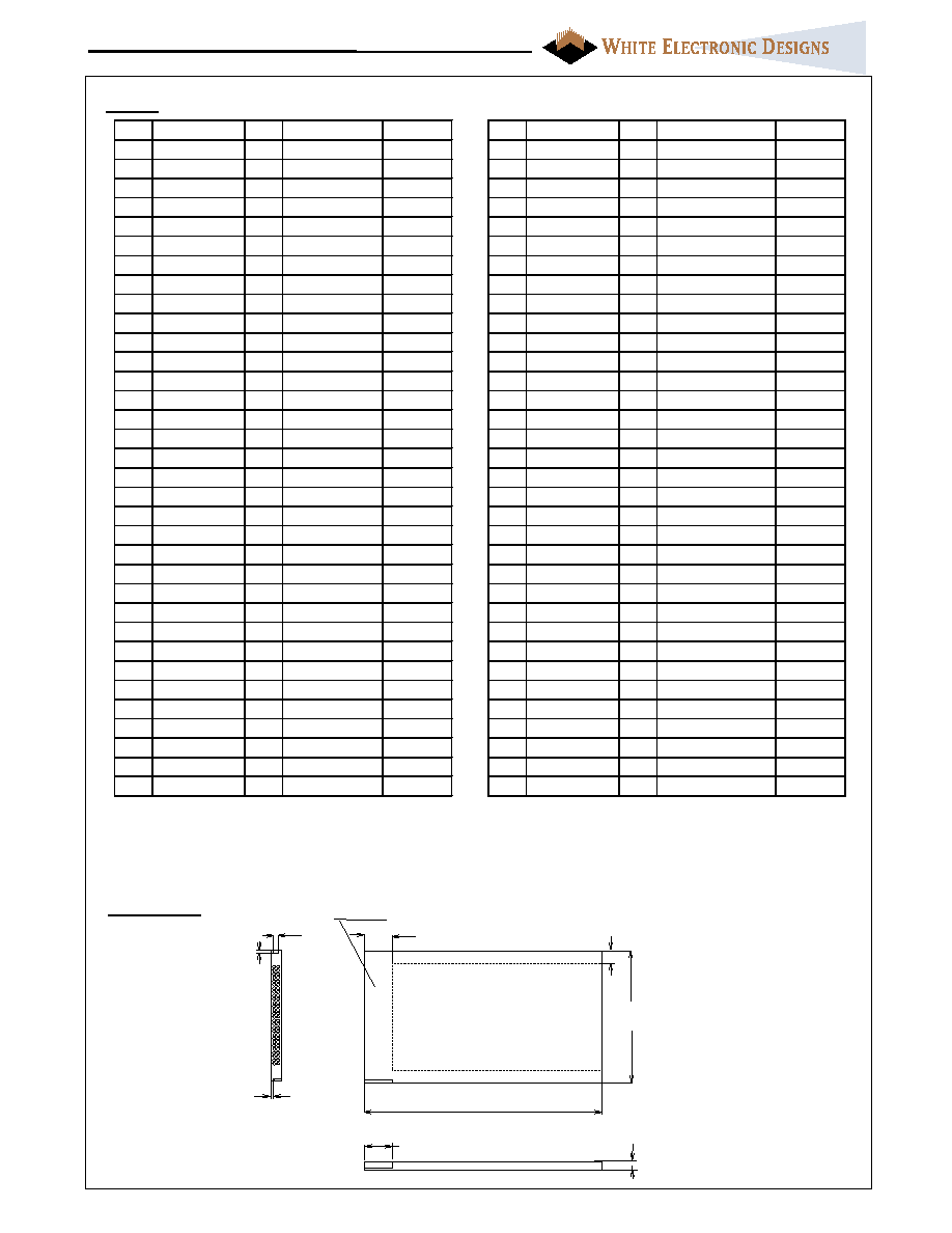
Mechanical
54.0mm ± 0.10
(2.126")
10.0mm MIN
(0.400")
1.6mm ± 0.05
(0.063")
1.0mm ± 0.05
(0.039")
1.0mm ± 0.05
(0.039")
3.3mm ± T1 (0.130")
T1=0.10mm interconnect area
T1=0.20mm substrate area
Interconnect area
10.0mm MIN
(0.400")
3.0mm MIN
85.6mm ± 0.20
(3.370")
Substrate area

August 2000 Rev. 3 - ECO #13134
3
PCMCIA Flash Memory Card
FVA Series
PC Card Products
Symbol
Type
Name and Function
A0 - A25
INPUT
ADDRESS INPUTS: A0 through A25 enable direct addressing of
up to 64MB of memory on the card. Signal A0 is not decoded since
the card is x16 only. The memory will wrap at the card density
boundary. The system should not try to access memory beyond the
card density. The upper addresses are not connected.
DQ0 - DQ15
INPUT/OUTP
UT
DATA INPUT/OUTPUT: DQ0 THROUGH DQ15 constitute the
bi-directional databus. DQ0 - DQ7 constitute the lower (even) byte
and DQ8 - DQ15 the upper (odd) byte. DQ15 is the MSB.
CE1#, CE2#
INPUT
CARD ENABLE 1 AND 2: CE1# enables even byte accesses, CE2#
enables odd byte accesses. Odd byte (DQ8 - DQ15) can not be
accessed on DQ0 - DQ7.
OE#
INPUT
OUTPUT ENABLE: Active low signal enabling read data from the
memory card.
WE#
INPUT
WRITE ENABLE: Active low signal gating write data to the
memory card.
RDY/BSY#
OUTPUT
READY/BUSY OUTPUT: Indicates status of internally timed erase
or program algorithms. A high output indicates that the card is ready
to accept accesses.
CD1#, CD2#
OUTPUT
CARD DETECT 1 and 2: Provide card insertion detection. These
signals are connected to ground internally on the memory card. The
host socket interface circuitry shall supply 10K-ohm or larger pull-up
resistors on these signal pins.
WP
OUTPUT
WRITE PROTECT: This signal is pulled low internally. This
signifies write protect = "off " for all cases.
VPP1, VPP2
N.C.
PROGRAM/ERASE POWER SUPPLY: Not connected for 5V
only card.
VCC
CARD POWER SUPPLY: 5.0V for all internal circuitry.
GND
GROUND: for all internal circuitry.
REG#
INPUT
ATTRIBUTE MEMORY SELECT : only used with cards built
with optional attribute memory.
RST
INPUT
RESET: Active high signal for placing card in Power-on default
state. Reset can be used as a Power-Down signal for the memory
array.
WAIT#
OUTPUT
WAIT: This signal is pulled high internally for compatibility. No
wait states are generated.
BVD1, BVD2
OUTPUT
BATTERY VOLTAGE DETECT: These signals are pulled high to
maintain SRAM card compatibility.
VS1, VS2
OUTPUT
VOLTAGE SENSE: Notifies the host socket of the card's VCC
requirements. VS1 and VS2 are open to indicate a 5V, 16 bit card
has been inserted.
RFU
RESERVED FOR FUTURE USE
N.C.
NO INTERNAL CONNECTION TO CARD: pin may be driven
or left floating
Card Signal Description
READ function
Common Memory
Attribute Memory
Function Mode
/CE2 /CE1
/OE
/WE
/REG D15-D8
D7-D0
/REG D15-D8
D7-D0
Standby Mode
H
H
X
X
X
High-Z
High-Z
X
High-Z
High-Z
Low Byte Access
H
L
L
H
H
High-Z
Even-Byte
L
High-Z
Even-Byte
Word Access (16 bits)
L
L
L
H
H
Odd-Byte Even-Byte
L
Not Valid
Even-Byte
Odd-Byte Only Access
L
H
L
H
H
Odd-Byte
High-Z
L
Not Valid
High-Z
WRITE function
Standby Mode
H
H
X
X
X
X
X
X
X
X
Low Byte Access
H
L
H
L
H
X
Even-Byte
L
X
Even-Byte
Word Access (16 bits)
L
L
H
L
H
Odd-Byte Even-Byte
L
X
Even-Byte
Odd-Byte Only Access
L
H
H
L
H
Odd-Byte
X
L
X
X
Functional Truth Table

August 2000 Rev. 3 - ECO #13134
4
PCMCIA Flash Memory Card
FVA Series
PC Card Products
Absolute Maximum Ratings
(2)
Operating Temperature TA (ambient)
Commercial
0∞C to +60 ∞C
Industrial
-40∞C to +85 ∞C
Storage Temperature
-55∞C to +110 ∞C
Voltage on any pin relative to VSS
-0.5V to VCC+0.5V (1)
VCC supply Voltage relative to VSS
-0.5V to +7.0V
Notes:
(1) During transitions, inputs may undershoot
to -2.0V or overshoot to VCC +2.0V for
periods less than 20ns.
(2) Stress greater than those listed under
"Absolute Maximum ratings" may cause
permanent damage to the device. This is a
stress rating only and functional operation at
these or any other conditions greater than
those indicated in the operational sections of
this specification is not implied. Exposure to
absolute maximum rating conditions for
extended periods may affect reliability.
Symbol Parameter
Density
(Mbytes)
Notes
Typ
(3)
Max
Units
Test Conditions
ICCR
VCC Read Current
2,4,8,16
75
mA
VCC = 5.25V
tcycle = 100ns
ICCW
VCC Program Current
2,4,8,16
100
mA
ICCE
VCC Erase Current
2,4,8,16
100
mA
ICCSL
VCC Sleep Current
2,4,8
2
50
160
µA
VCC = 5.25V
Control Signals = VCC
Reset = VIH
ICCSL
VCC Sleep Current
16
2
90
240
µA
VCC = 5.25V
Control Signals = VCC
Reset = VIH
ICCS
VCC Standby Current
2,4,8,16
2
3
10
mA
VCC = 5.25V
Control Signals = VCC
Notes:
1. All currents are for x16 mode and are RMS values unless otherwise specified.
2. Control Signals: CE
1
#, CE
2
#, OE#, WE#, REG#.
3. Typical: VCC = 5V, T = +25C.
CMOS Test Conditions: VIL = VSS ± 0.2V, VIH = VCC ± 0.2V
DC Characteristics
(1)
Symbol
Parameter
Notes
Min
Max
Units
Test Conditions
ILI
Input Leakage Current
1,2
±20
µA
VCC = VCCMAX
Vin =VCC or VSS
ILO
Output Leakage Current
1
±20
µA
VCC = VCCMAX
Vout =VCC or VSS
VIL
Input Low Voltage
1
0
0.8
V
VIH
Input High Voltage
1
3.85
VCC+0.5
V
VOL
Output Low Voltage
1
0.4
V
IOL = 3.2mA
VOH
Output High Voltage
1
VCC-0.4
VCC
V
IOH = -2.0mA
VLKO
VCC Erase/Program
Lock Voltage
1
2.0
V
Notes:
1. Values are the same for byte and word wide modes for all card densities.
2. Exceptions: Leakage currents on CE1#, CE2#, OE#, REG# and WE# will be < 500 µA when VIN = GND due to
internal pull-up resistors. Leakage currents on RST will be <150µA when VIN=VCC due to internal pull-down resistor.

August 2000 Rev. 3 - ECO #13134
5
PCMCIA Flash Memory Card
FVA Series
PC Card Products
N O TE 1
N O TE 1
A[25::0], /R E G
/C E1, /C E2
/O E
D[15::0]
tc(R )
ta(A )
th(A )
tv(A )
ta(C E )
tsu(C E )
th(C E)
ten(O E)
ta(O E )
tsu(A)
D A TA V ALID
tdis(C E )
tdis(O E )
100ns (2)
150ns
SYMBOL
(PCMCIA)
Parameter
Min
Max
Min
Max
Unit
t
C
(R)
Read Cycle Time
100
150
ns
t
a
(A)
Address Access Time
100
150
ns
t
a
(CE)
Card Enable Access Time
100
150
ns
t
a
(OE)
Output Enable Access Time
50
75
ns
t
su
(A)
Address Setup Time
10
20
ns
t
su
(CE)
Card Enable Setup Time
0
0
ns
t
h
(A)
Address Hold Time
15
20
ns
t
h
(CE)
Card Enable Hold Time
15
20
ns
t
v
(A)
Output Hold from Address Change
0
0
ns
t
dis
(CE)
Output Disable Time from CE#
50
75
ns
t
dis
(OE)
Output Disable Time from OE#
50
75
ns
t
en
(CE)
Output Enable Time from CE#
5
5
ns
t
en
(OE)
Output Enable Time from OE#
5
5
ns
trec(RST)
Power Down recovery to Output
Delay. VCC = 5V
500
500
ns
AC Characteristics
Notes:
1. AC timing diagrams and characteristics are guaranteed to meet or exceed PCMCIA 2.1 specifications.
2. Valid for cards using 8Mb components (28F008SA or 28F008S5)only. Cards based on 16Mb (28F016)
are available as 150ns cards only.
Read Timing Diagram
Read Timing Parameters
(1)
Note: Signal may be high or low in this area.