
October 2001 Rev. 1 - ECO #xxxxx
1
PCMCIA Flash Memory Card
FVF Series
PC Card Products
Features
∑ PCMCIA 2.1 (PC Card 97) compatible
- Type I or Type II Form Factor
∑ Low cost Linear Flash Card
∑ Single Supply Operation
∑ FVF0x - 5V
∑ FVF1x - 5V or 3.3V (Note 1)
∑ Fast Read Performance
- 200ns Maximum Access Time
∑ Based on MLC Strata Flash Components
∑ Common Flash Interface (CFI) compliant
∑ High Performance Random Writes
- 6µs Typical per Byte Write Time, using 32Byte
Write buffer
∑ Automated Write and Erase Algorithms
∑ High Write/Erase Endurance:
100,000 Write/Erase Cycles
∑ Low Power Consumption
∑ 150µA Standby Current
∑ 75mA Max Byte Write Current
The FVF Value Series Flash memory cards offer a low cost
linear Flash solid state storage solution for code and data
storage, high performance disk emulation, mobile PC and
embedded applications.
FVF series cards offer memory capacities from 4MB to
64MB, with 128kB block erase size.
The WEDC Value series is based on Intel MLC, Strata Flash
memories. Cards are based on the two families of memory
components:
FVF0x built with: 28F640J5, 28F320J5
FVF1x built with: 28F128J3, 28F640J3, 28F320J3
These flash devices support the Common Flash Interface
(CFI) programming algorithm, a standard that allows system
level software to evaluate the flash configuration, electrical
characteristic, programming parameters and supported
functions. CFI is intended to support future upgrades with
universal programming algorithms, so there is no longer a
need for continued programming software modification and
updates. Systems should be able to recognize and support all
devices to allow universal expansion/upgrade path.
The symmetrically blocked architecture and single supply
(5V for FVF0x and universal 3.3V or 5V for FVF1x cards)
operation provides a cost effective, high performance,
nonvolatile storage solution. The PC Card form factor offers
an industry standard pinout and mechanical outline, allowing
density upgrades without system design changes.
The Value series is designed as a simple x16 linear array of
Flash devices. One Flash device provides the lower and
upper bytes for the 16 bit access. Other modes of operation
are also supported (See Functional Truth Table on page 5)
WEDC's standard Value Series Flash Card is shipped with
no attribute memory or CIS (Card Information Structure)
information. An option for 2KB of attribute memory with
CIS information is available. The CIS for the WEDC Value
series may also be stored in Block 0 (even bytes, D0 - D7
only) of the Flash memory. This option is available by
request only.
WEDC's standard cards are shipped with WEDC's Logo.
Cards are also available with blank housings (no Logo). The
blank housings are available in both a recessed (for label)
and flat housing. Please contact WEDC sales representative
for further information on Custom artwork.
FVF Value Series Flash Memory Card 4, 8, 16, 32, 48 and 64MB(Intel Strata Flash )
General Description
Note 1:
FVF1x supports wide, universal operating
voltage: 3V to 5V.
That means the card will work in 3.3V systems
as well as in 5V systems. This feature may
allow easy exchange of data between multiple
and different systems and provide easy
upgrade / expansion path.

October 2001 Rev. 1 - ECO #xxxxx
2
PCMCIA Flash Memory Card
FVF Series
PC Card Products
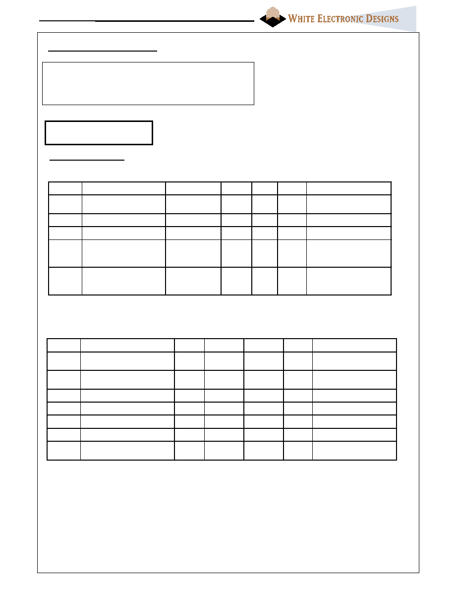
FVF block diagram
Addresses
A1..A25
(note 1)
DATA Low
D7..0
28F640J5
28F320J5
28F128J3
28F640J3
28F320J3
D7..0
Memory
Low Byte
PCMCIA in
terface
D15..8
Memory
High Byte
Buffers and Cont
rol logic
Addresses
A1..A25
Attribute Memory
(optional)
DATA Low
D15..8
RDY/BSY#
/CS0
/CS1
/CSn
/CE
/CE
/CE
R/B /PD
Reset
Circuit
Vcc
RST
BVD2
BVD1
Notes:
1.
A25..23 pulled down by 100k
resistors
2.
Open for FVF0x;
GND for FVF1x (3.3V operation)
VS1
VS2
open
open/GND
(note 2)
CD2
CD1
CE2#
CE1#
WE#
OE#
- pull down resistor Typ. 100k
- pull up resistor Min. 10k
Manufacturer and Device ID codes
Device
Manuf ID Device ID
Int 28F128J3
89h
18h
Int 28F640J3
89h
17h
Int 28F320J3
89h
16h
Int 28F640J5
89h
15h
Int 28F320J5
89h
14h

October 2001 Rev. 1 - ECO #xxxxx
3
PCMCIA Flash Memory Card
FVF Series
PC Card Products
For information regarding modes of operation, commands, and programming
details for the memory components, please consult the Intel 28F128J3A,
28F640J5 data sheets.
Writing commands to the CUI enables reading of device data, query, identifier codes, inspection and clearing of the
status register, and, when V
PEN
= V
PENH
, block erasure, program, and lock-bit configuration.
The Block Erase command requires appropriate command data and an address within the block to be erased. The
Byte/Word Program command requires the command and address of the location to be written. Set Block Lock-Bit
commands require the command and block within the device to be locked. The Clear Block Lock-Bits command
requires the command and address within the device.
The CUI does not occupy an addressable memory location. It is written when the device is enabled and WE# is
active. The address and data needed to execute a command are latched on the rising edge of WE# or the first edge
of CE1# or CE2# that disables the card. Standard microprocessor write timings are used.

October 2001 Rev. 1 - ECO #xxxxx
4
PCMCIA Flash Memory Card
FVF Series
PC Card Products
1
GND
Ground
35
GND
Ground
2
DQ3
I/O
Data bit 3
36
CD1#
O
Card Detect 1
LOW
3
DQ4
I/O
Data bit 4
37
DQ11
I/O
Data bit 11
4
DQ5
I/O
Data bit 5
38
DQ12
I/O
Data bit 12
5
DQ6
I/O
Data bit 6
39
DQ13
I/O
Data bit 13
6
DQ7
I/O
Data bit 7
40
DQ14
I/O
Data bit 14
7
CE1#
I
Card enable 1
LOW
41
DQ15
I
Data bit 15
8
A10
I Address bit 10
42
CE2#
I
Card Enable 2
LOW
9
OE#
I
Output enable
LOW
43
VS1
O
Voltage Sense 1 N.C.or GND (2)
10
A11
I Address bit 11
44
RFU
Reserved
11
A9
I
Address bit 9
45
RFU
Reserved
12
A8
I
Address bit 8
46
A17
I
Address bit 17
13
A13
I Address bit 13
47
A18
I
Address bit 18
14
A14
I Address bit 14
48
A19
I
Address bit 19
15
WE#
I
Write Enable
LOW
49
A20
I
Address bit 20
16 RDY/BSY# O
Ready/Busy
LOW (1)
50
A21
I
Address bit 21
17
Vcc
Supply Voltage
51
Vcc
Supply Voltage
18
Vpp1
Prog. Voltage
N.C.
52
Vpp2
Prog. Voltage
N.C.
19
A16
I Address bit 16
53
A22
I
Address bit 22
20
A15
I Address bit 15
54
A23
I
Address bit 23
21
A12
I Address bit 12
55
A24
I
Address bit 24
22
A7
I
Address bit 7
56
A25
I
Address bit 25
23
A6
I
Address bit 6
57
VS2
O
Voltage Sense 2
N.C.
24
A5
I
Address bit 5
58
RST
I
Card Reset
HIGH
25
A4
I
Address bit 4
59
Wait#
O Extended Bus cycle
LOW
26
A3
I
Address bit 3
60
RFU
Reserved
27
A2
I
Address bit 2
61
REG#
I
Attrib Mem Select N.C (optional)
28
A1
I
Address bit 1
62
BVD2
O Bat. Volt. Detect 2
29
A0
I
Address bit 0
63
BVD1
O Bat. Volt. Detect 1
30
DQ0
I/O
Data bit 0
64
DQ8
I/O
Data bit 8
31
DQ1
I/O
Data bit 1
65
DQ9
I/O
Data bit 9
32
DQ2
I/O
Data bit 2
66
DQ10
O
Data bit 10
33
WP
O
Write Potect
HIGH
67
CD2#
O
Card Detect 2
LOW
34
GND
Ground
68
GND
Ground
Pinout
Notes:
1. RDY/BSY signal is an open drain output, with MIN 47k
pull-up resistor.
2. N.C. for FVF0x (5V only operation)
GND for FVF1x (3.3V or 5V operation)
Mechanical
54.0mm ± 0.10
(2.126")
10.0mm MIN
(0.400")
1.6mm ± 0.05
(0.063")
1.0mm ± 0.05
(0.039")
1.0mm ± 0.05
(0.039")
3.3mm ± T1 (0.130")
T1=0.10mm interconnect area
T1=0.20mm substrate area
Interconnect area
10.0mm MIN
(0.400")
3.0mm MIN
85.6mm ± 0.20
(3.370")
Substrate area

October 2001 Rev. 1 - ECO #xxxxx
5
PCMCIA Flash Memory Card
FVF Series
PC Card Products
Symbol Type
Name
and
Function
A0 - A25
INPUT
ADDRESS INPUTS: A0 through A25 enable direct addressing of up to 64MB of
memory on the card. Signal A0 is used only in 8 bit configuration (CE1# active
CE2# not active). A0 is disregarded in 16 bit operation (CE1# and CE2# active).
The system should not try to access memory beyond the card density because the
card will return undefined data. (The upper addresses are decoded).
DQ0 - DQ15
INPUT /
OUTPUT
DATA INPUT/OUTPUT: DQ0 THROUGH DQ15 constitute the bi-directional
databus. DQ0 - DQ7 constitute the lower (even) byte and DQ8 - DQ15 the upper
(odd) byte. DQ15 is the MSB.
CE1#, CE2#
INPUT
CARD ENABLE 1 AND 2: CE1# enables even byte accesses, CE2# enables odd
byte accesses. (See below the Functional Truth Table).
OE# INPUT
OUTPUT ENABLE: Active low signal enabling read data from the memory card.
WE# INPUT
WRITE ENABLE: Active low signal gating write data to the memory card.
RDY/BSY# OUTPUT
READY/BUSY OUTPUT: Indicates status of internally timed erase or program
algorithms. A high output indicates that the card is ready to accept accesses.
CD1#, CD2#
OUTPUT
CARD DETECT 1 and 2: Provide card insertion detection. These signals are
connected to ground internally on the memory card. The host socket interface
circuitry shall supply 10K-ohm or larger pull-up resistors on these signal pins.
WP OUTPUT
WRITE PROTECT: This signal is pulled low internally. This signifies write
protect = "off " for all cases.
VPP1, VPP2
N.C.
PROGRAM/ERASE POWER SUPPLY: Not connected for 5V only card.
VCC
CARD POWER SUPPLY: (5.0V for FVF0x or 3V to 5V for FVF1x)
GND
GROUND:
REG# INPUT
ATTRIBUTE MEMORY SELECT: connected only on cards built with optional
attribute memory. (see Note 1)
RST INPUT
RESET: Active high signal for placing card in Power-on default state.
WAIT# OUTPUT
WAIT: This signal is pulled high internally for compatibility. No wait states are
generated.
BVD1, BVD2
OUTPUT
BATTERY VOLTAGE DETECT: These signals are pulled high to maintain
SRAM card compatibility.
VS1, VS2
OUTPUT
VOLTAGE SENSE: Notifies the host socket of the card's VCC requirements. VS1
and VS2 are open to indicate a 5V; VS1=GND and VS2 open indicate possibility
to work in 3.3V systems.
RFU
RESERVED FOR FUTURE USE
N.C.
NO INTERNAL CONNECTION TO CARD: pin may be driven or left floating
Card Signal Description
Notes:
1. For standard cards without Attribute memory this signal is not connected:
X ≠ don't care
2. Operation in Shaded row not supported: Accessing memory in this mode may alter data in lower byte
For proper operation signals CE1# and CE2# should be connected together (for 16 bit operation) or signal
CE2# should be always in High state (for 8bit operation)
3. Switching between byte access mode (8 bit) and word access mode (16 bit) requires a 1ms setup time.
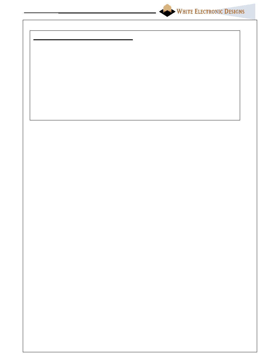
READ function
Common Memory
Attribute Memory (optional)
Function Mode
CE2# CE1# A0 OE# WE# REG# D15-D8
D7-D0 REG# D15-D8
D7-D0
Standby Mode
H
H
X
X
X
X High-Z High-Z X High-Z High-Z
Byte Access (8 bits) (3) H L L L H
H (1) High-Z Even-Byte
L High-Z
Even-Byte
H
L H L
H H (1) High-Z Odd-Byte
L High-Z
Not
Valid
Word Access (16 bits) (3) L L X L H
H (1) Odd-Byte Even-Byte
L Not
Valid Even-Byte
Odd-Byte Only Access
L
H
X
L
H
H (1) Odd-Byte High-Z
L Not
Valid High-Z
WRITE function
Standby Mode
H
H
X
X
X
X X
X X X
X
Byte Access (8 bits) (3)
H L L H L
H (1) X Even-Byte
L X
Even-Byte
H L H H L
H (1) X Odd-Byte
L X
X
Word Access (16 bits) (3) L L X H L H (1) Odd-Byte Even-Byte
L X
Even-Byte
Odd-Byte Only Access (2)
L
H
X
H
L
H (1) Odd-Byte
X
L
X
X
Functional Truth Table
October 2001 Rev. 1 - ECO #xxxxx
6
PCMCIA Flash Memory Card
FVF Series
PC Card Products
Absolute Maximum Ratings
(1)
Operating Temperature TA (ambient)
Commercial
0∞C to +70 ∞C
Storage Temperature
-55∞C to +110 ∞C
Voltage on any pin relative to VSS
-0.5V to VCC+0.5V
Notes:
(1) Stress greater than those listed under
"Absolute Maximum ratings" may cause
permanent damage to the device. This is a
stress rating only and functional operation at
these or any other conditions greater than
those indicated in the operational sections of
this specification is not implied. Exposure to
absolute maximum rating conditions for
extended periods may affect reliability.
Symbol Parameter
Notes
Typ(1) Max Units Test
Conditions
ICCR
VCC Read Current
8 bit mode
16 bit mode
20
35
35
65
mA
VCC = VCC MAX
tcycle = 200ns
ICCW
VCC Program Current
1 device active
40
70
mA
ICCE
VCC Erase Current
1 device active
40
80
mA
ICCSL
VCC Sleep Current
Per device
80
125
µA
VCC = 5.25V
Control Signals = VCC
Reset = VIH (active)
ICCS
VCC Standby Current
Per device
CMOS inputs
150
µA
VCC
=
5.25V
Control Signals = VCC
Reset = VIL (not active)
Notes:
1. Typical: VCC = 5V, T = +25C.
CMOS Test Conditions: VIL = VSS ± 0.2V, VIH = VCC ± 0.2V
DC Characteristics
Symbol Parameter Notes
Min
Max
Units
Test
Conditions
ILI
Input Leakage Current
1, 2
±20
µA
VCC = VCCMAX
Vin =VCC or VSS
ILO
Output Leakage Current
1
±20
µA
VCC = VCCMAX
Vout =VCC or VSS
VIL Input
Low
Voltage
1 0
0.8 V
VIH
Input High Voltage
1
2.0
VCC+0.5
V
VOL
Output Low Voltage
1
0.4
V
IOL = 2mA
VOH
Output High Voltage
1
2.4
VCC
V
IOH = -2.0mA
VLKO VCC
Erase/Program
Lock Voltage
1 3.25 V
Notes:
1. Values are the same for byte and word wide modes for all card densities.
2. Exceptions: Leakage currents on CE1#, CE2#, OE#, REG# and WE# will be < 500 µA when VIN = GND due to
internal pull-up resistors. Leakage currents on RST will be <150µA when VIN=VCC due to internal pull-down resistor.
FVF0x Series
VCC supply voltage 5V

October 2001 Rev. 1 - ECO #xxxxx
7
PCMCIA Flash Memory Card
FVF Series
PC Card Products
Symbol Parameter
Notes
Typ
Max Units Test
Conditions
ICCR
VCC Read Current
16 bit mode
VCC = 3.3V
VCC = 5.0V
35
45
55
65
mA
VCC = VCC MAX
tcycle = 200ns
ICCW
VCC Program Current
VCC = 3.3V
VCC = 5.0V
35
40
60
70
mA
1 device active
ICCE
VCC Erase Current
VCC = 3.3V
VCC = 5.0V
35
40
70
80
mA
1 device active
ICCSL
VCC Sleep Current
Per device
80
125
µA
VCC = 3.3V
Control Signals = VCC
Reset = VIH (active)
ICCS
VCC Standby Current
Per device
TTL inputs
150
µA
VCC = 3.3V
Control Signals = VIH
Reset = VIL (not active)
CMOS Test Conditions: VIL = VSS ± 0.2V, VIH = VCC ± 0.2V
DC Characteristics
(1)
Symbol Parameter Notes
Min
Max
Units
Test
Conditions
ILI
Input Leakage Current
1, 2
±20
µA
VCC = VCCMAX
Vin =VCC or VSS
ILO
Output Leakage Current
1
±20
µA
VCC = VCCMAX
Vout =VCC or VSS
VIL Input
Low
Voltage
1 0
0.8 V
VIH
Input High Voltage
1
2.0
VCC+0.5
V
VOL
Output Low Voltage
1
0.4
V
IOL = 2mA
VOH
Output High Voltage
1
2.4
3.2
V
IOH = -2.0mA
VLKO VCC
Erase/Program
Lockout Voltage
1 2.0 V
Notes:
1. Values are the same for byte and word wide modes for all card densities.
2. Exceptions: Leakage currents on CE1#, CE2#, OE#, REG# and WE# will be < 500 µA when VIN = GND due to
internal pull-up resistors. Leakage currents on RST will be <150µA when VIN=VCC due to internal pull-down resistor.
FVF1x Series
VCC supply voltage 3V - 5V
VCC supply voltage 3V - 5V

October 2001 Rev. 1 - ECO #xxxxx
8
PCMCIA Flash Memory Card
FVF Series
PC Card Products
N O T E 1
N O T E 1
A[25::0], /REG
/CE 1, /CE2
/O E
D[15::0]
tc(R)
ta(A)
th(A)
tv(A)
ta(CE)
tsu(CE )
th(CE)
ten(O E)
ta(O E)
tsu(A)
DATA VA LID
tdis(CE)
tdis(O E)
200ns
250ns
SYMBOL
(PCMCIA)
Parameter
Min Max Min Max Unit
t
C
(R)
Read Cycle Time
200
250
ns
ta(A)
Address Access Time
200
250
ns
ta(CE)
Card Enable Access Time
200
250
ns
ta(OE)
Output Enable Access Time
100
125
ns
tsu(A) Address
Setup
Time
20 20
ns
tsu(CE) Card
Enable
Setup
Time
0 0
ns
th(A)
Address Hold Time
20
20
ns
th(CE)
Card Enable Hold Time
20
20
ns
tv(A) Output
Hold
from
Address
Change
0 0
ns
tdis(CE)
Output Disable Time from CE#
90
100
ns
tdis(OE)
Output Disable Time from OE#
90
100
ns
ten(CE) Output
Enable
Time
from
CE# 5 5
ns
ten(CE) Output
Enable
Time
from
OE# 5 5
ns
t
rec(RST)
Power Down recovery to Output
Delay. VCC = 5V
500
500
ns
AC Characteristics
Notes:
1. AC timing diagrams and characteristics are guaranteed to meet or exceed PCMCIA 2.1 specifications.
Read Timing Diagram
Read Timing Parameters
(1)
Note: Signal may be high or low in this area.

October 2001 Rev. 1 - ECO #xxxxx
9
PCMCIA Flash Memory Card
FVF Series
PC Card Products
200ns
250ns
SYMBOL
(PCMCIA)
Parameter
Min Max Min Max Unit
tCW
Write Cycle Time
200
250
ns
tw(WE)
Write Pulse Width
120
150
ns
tsu(A)
Address Setup Time
20
30
ns
tsu(A-WEH)
Address Setup Time for WE#
140
180
ns
tsu(CE-WEH)
Card Enable Setup Time for WE#
140
180
ns
tsu(D-WEH)
Data Setup Time for WE#
60
80
ns
th(D)
Data Hold Time
30
30
ns
trec(WE)
Write Recover Time
30
30
ns
tdis(WE)
Output Disable Time from WE#
90
100
ns
tdis(OE)
Output Disable Time from OE#
90
100
ns
ten(WE)
Output Enable Time from WE#
5
5
ns
ten(OE)
Output Enable Time from OE#
5
5
ns
tsu(OE-WE)
Output Enable Setup from WE#
10
10
ns
th(OE-WE)
Output Enable Hold from WE#
10
10
ns
tsu(CE)
Card Enable Setup Time from OE#
0
0
ns
th(CE)
Card Enable Hold Time
20
20
ns
Notes:
1. AC timing diagrams and characteristics are guaranteed to meet or exceed PCMCIA 2.1 specifications.
Write Timing Diagram
Write Timing Parameters
(1)
th (O E - W E )
N O T E 1
/C E 1 , /C E 2
N O T E 1
ts u ( C E - W E H )
tc (W )
A [2 5 ::0 ], /R E G
tw (W E )
td is ( W E )
th (D )
D [1 5 ::0 ]( D in )
D A T A IN P U T
ts u ( A )
ts u ( A - W E H )
/O E
ts u ( C E )
ts u ( D -W E H )
tre c (W E )
th (C E )
ts u ( O E - W E )
td is ( O E )
D [1 5 ::0 ]( D o u t)
te n ( O E )
te n ( W E )
N O T E 2
N O T E 2
/W E
Notes:
1. Signal may be high or low in this area.
2. When the data I/O pins are in the output state, no signals shall be applied to the data pins (D15 - D0) by the host system.

October 2001 Rev. 1 - ECO #xxxxx
10
PCMCIA Flash Memory Card
FVF Series
PC Card Products
Parameter Notes
Min
Typ
(1)
Max Units
Write Buffer Byte program time
(time to prog. 32Bytes/16Words)
- J5 device
- J3 device
218
200
654
TBD
µs
Byte Program time
-Using Word/Byte prog command
- J5 device
- J3 device
210
180
630
TBD
µs
Block Program Time
128kB written using Write to Buffer
- J5 device
- J3 device
0.8
0.8
2.4
TBD
sec
Block Erase Time
- J5 device
- J3 device
1
0.7
5
TBD
sec
Data Write and Erase Performance
(1, 2, 3 ,4)
Notes:
1. Typical: Nominal voltages and T
A
= 25C.
2. Excludes system overhead.
3. Valid for all speed options.
4. To maximize system performance, RDY/BSY# signal or component status register should be polled.
FVF0x: VCC = 5V ± 5%,
FVF1x: VCC = 3V ≠ 5V

October 2001 Rev. 1 - ECO #xxxxx
11
PCMCIA Flash Memory Card
FVF Series
PC Card Products
EDI
Company Name
Lot code / trace number
Date code
Part number
PRODUCT MARKING
WED 7P016FVF0100C20 C995 9915
Note:
Some products are currently marked with our pre-merger company name/acronym (EDI). During our
transition period, some products will also be marked with our new company name/acronym (WED).
Starting October 2001 all PCMCIA products will be marked only with the WED prefix.
Card capacity
016 16MB
Packaging option
00
Standard, type 1
PC card
P
Standard PCMCIA
R
Ruggedized PCMCIA
Card family and version
- See Card Family and Version Info. for details (next page)
Temperature range
C Commercial 0∞C to +70∞C
I Industrial -40∞C to +85∞C
Card access time
20
200ns
25
250ns
Card technology
7
FLASH
8
SRAM
PART NUMBERING
7 P 016 FVF01 00 C 20

October 2001 Rev. 1 - ECO #xxxxx
12
PCMCIA Flash Memory Card
FVF Series
PC Card Products
7P XXX FVF YY SS T ZZ
where
XXX:
004
4MB (built with 28F320)
008
8MB
016
16MB
032
32MB
048
48MB
064
64MB
YY:
01
J5 based (28F640J5, 28F320J5)
02
J5 based with attribute memory ≠ not available
11
J3 based (28F128J3, 28F640J3, 28F320J3
12
J3 with attribute memory ≠ not available
SS:
00
WEDC Silkscreen
01
Blank Housing, Type I
02
Blank Housing, Type I Recessed
T:
C
Commercial
ZZ:
20
200ns
25
250ns
Ordering Information
Part Number Table - Common Options
Notes:
1. Other options, including density, architecture and speed are available, please contact your WEDC sales representative
with your request.
WEDC Part Number
Density
Speed
Flash Component
Attribute Memory
Intel Strata Flash Based Cards
7P004FVF0100C20
4MB
200ns
28F320J5
NO
7P008FVF0100C20
8MB
200ns
28F6400J5
NO
7P064FVF0100C20
64MB
200ns
28F640J5
NO
7P016FVF1100C20
16MB
200ns
28F128J3
NO
7P064FVF1100C20
64MB
200ns
28F128J3
NO
October 2001 Rev. 1 - ECO #xxxxx
13
PCMCIA Flash Memory Card
FVF Series
PC Card Products
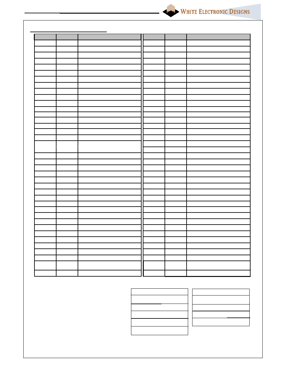
Card Information Structure (CIS)
The CIS is an information describing the PCMCIA card's functionality and structure. This
information can be used by host system to determine programming requirements, needed
resources to access the card, etc.
This information is stored in the form of binary data in separate memory (Attribute memory), or in
the first block of main (common) memory. Data is stored only on the lower data byte only (D7..0).
Upper byte (D15..8) is disregarded and its value is undefined. Cards built with separate Attribute
memory have signal REG# connected: when active, it enables Attribute memory and allows access
to CIS data.
Cards without Attribute memory do not contain any CIS data: they are shipped "blank" with FFhex
data. For client's request, data can be programmed to common memory (see below for CIS data).
For detail information about CIS structure please refer to PCMCIA standard (Metaformat
Specification).
October 2001 Rev. 1 - ECO #xxxxx
14
PCMCIA Flash Memory Card
FVF Series
PC Card Products
CIS Data ≠ (example/reference)
Address
Value
Description
Address
Value
Description
00H
01H CISTPL_DEVICE
4CH
20H
SPACE
02H
03H
TPL_LINK
4EH
53H
S
04H
52H
FLASH = 200ns (device writable)
50H
45H
E
06H
FEH
CARD SIZE: 64MB (note 1)
52H
52H
R
08H
FFH
END OF DEVICE
54H
49H
I
0AH
18H CISTPL_JEDEC_C
56H
45H
E
0CH
03H
TPL_LINK
58H
53H
S
0EH
89H
Manufacturer ID - INTEL
5AH
00H
END TEXT
10H
18H
Device ID - 28F0128J3A (note 2)
5CH
49H
I
12H
FFH
END OF DEVICE
5EH
4EH
N
14H
1EH CISTPL_DEVICEGEO
60H
54H
T
16H
07H
TPL_LINK
62H
45H
E
18H
02H
DGTPL_BUS (2 Bytes)
64H
4CH
L
1AH
11H
DGTPL_EBS (128kB)
66H
20H
SPACE
1CH
01H
DGTPL_RBS
68H
53H
S
1EH
01H
DGTPL_WBS
6AH
54H
T
20H
01H
DGTPL_PART
6CH
52H
R
22H
01H
FLASH DEVICE
6EH
41H
A
NON-INTERLEAVED
70H
54H
T
24H
FFH
END OF TUPLE
72H
41H
A
26H
15H
CISTPL_VERS1
74H
20H
SPACE
28H
7FH
TPL_LINK
76H
46H
F
2AH
04H
TPLLV1_MAJOR
78H
4CH
L
2CH
01H
TPLLV1_MINOR
7AH
41H
A
2EH
57H
W
7CH
53H
S
30H
48H
H
7EH
48H
H
32H
49H
I
80H
00H
END TEXT
34H
54H
T
82H
00H
END string
36H
45H
E
84H
FFH
END OF TUPLE
38H
20H
SPACE
86H
FFH
3AH
45H
E
88H
FFH
3CH
44H
D
8AH
FFH
3EH
43H
C
8CH
FFH
40H
20H
END TEXT
8EH
FFH
42H
46H
F
90H
FFH
44H
56H
V
92H
FFH
46H
46H
F
48H
30H
31H
0
1
4AH
X
Notes:
1. Value depends on card capacity: refer
to the capacity table on the right
2. Value depends on component type
used: refer to the device ID table on the
right
Device
Device ID
Int 28F128J3
18h
Int 28F640J3
17h
Int 28F320J3
16h
Int 28F640J5
15h
Int 28F320J5
14h
Card Capacity
Value
8MB
1Eh
16MB
3Eh
24MB
5Eh
32MB
7Eh
48MB
BEh
64MB
FEh
October 2001 Rev. 1 - ECO #xxxxx
15
PCMCIA Flash Memory Card
FVF Series
PC Card Products
revision
rev date
description
0
Oct-00 initial release
1
Oct-01 final release
Revision History
White Electronic Designs Corporation
One Research Drive, Westborough, MA 01581, USA
tel:
(508) 366 5151
fax: (508) 836 4850
www.whiteedc.com