 | –≠–ª–µ–∫—Ç—Ä–æ–Ω–Ω—ã–π –∫–æ–º–ø–æ–Ω–µ–Ω—Ç: SRV | –°–∫–∞—á–∞—Ç—å:  PDF PDF  ZIP ZIP |
June 2000 Rev. 1 - ECO #12896
1
PCMCIA Flash Memory Card
SRV Series
PC Card Products
Features
∑
High Performance SRAM memory Card
∑ Universal 3.3 to 5 Volt Supply allows for wider
compatibility between systems.
∑ Fast Access times: 150ns @ 5V
250ns @ 3.3V
∑ x8/x16 PCMCIA standard interface
∑ Low Power CMOS technology provides very low
power and reliable data retention characteristics
- standby current < 100µA typical
∑ Rechargeable Lithium battery with recharge circuitry
- eliminates the need for replaceable batteries
- standby current during recharge typically < 2mA
- battery backup time
∑7 months - type I card
∑18 months - type II card
typical based on 4MB (lower densities will
have greater storage times)
∑ Unlimited write cycles, no endurance issues
∑ Optional Features:
∑ 2KB EEPROM attribute memory containing
CIS
∑ Optional Hardware Write Protect switch
∑ PC Card Standard Type I or Type II Form Factor
The WEDC SRAM Series (SRV) memory cards
offer a high performance nonvolatile storage solution
for code and data storage, disk caching, and write
intensive mobile and embedded applications.
Packaged in PCMCIA type I or type II housing (type
II for cards with extended battery backup time and
8MB cards), the WEDC SRAM SRV series is based
on 1 or 4Mbit SRAM
memories, providing densities
from 256 Kilobytes to 8 Megabytes.
The SRV series of SRAM memory cards is a
universal 3V/ 5V power supply and operates at
speeds as high as 150ns. The cards are based on
advanced CMOS technology providing very low
power and reliable data retention characteristics.
WEDC's SRAM cards contain a rechargeable
lithium battery and recharge circuitry, eliminating the
need for replaceable batteries found in many SRAM
cards.
WEDC's standard cards are shipped with WEDC's
SRAM Logo. Cards are also available with blank
housings (no Logo). The blank housings are available
in both a recessed (for label) and flat housing. Please
contact WEDC sales representative for further
information on Custom artwork.
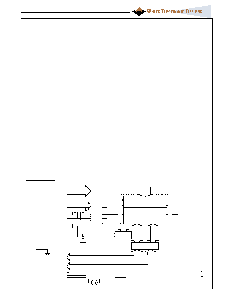
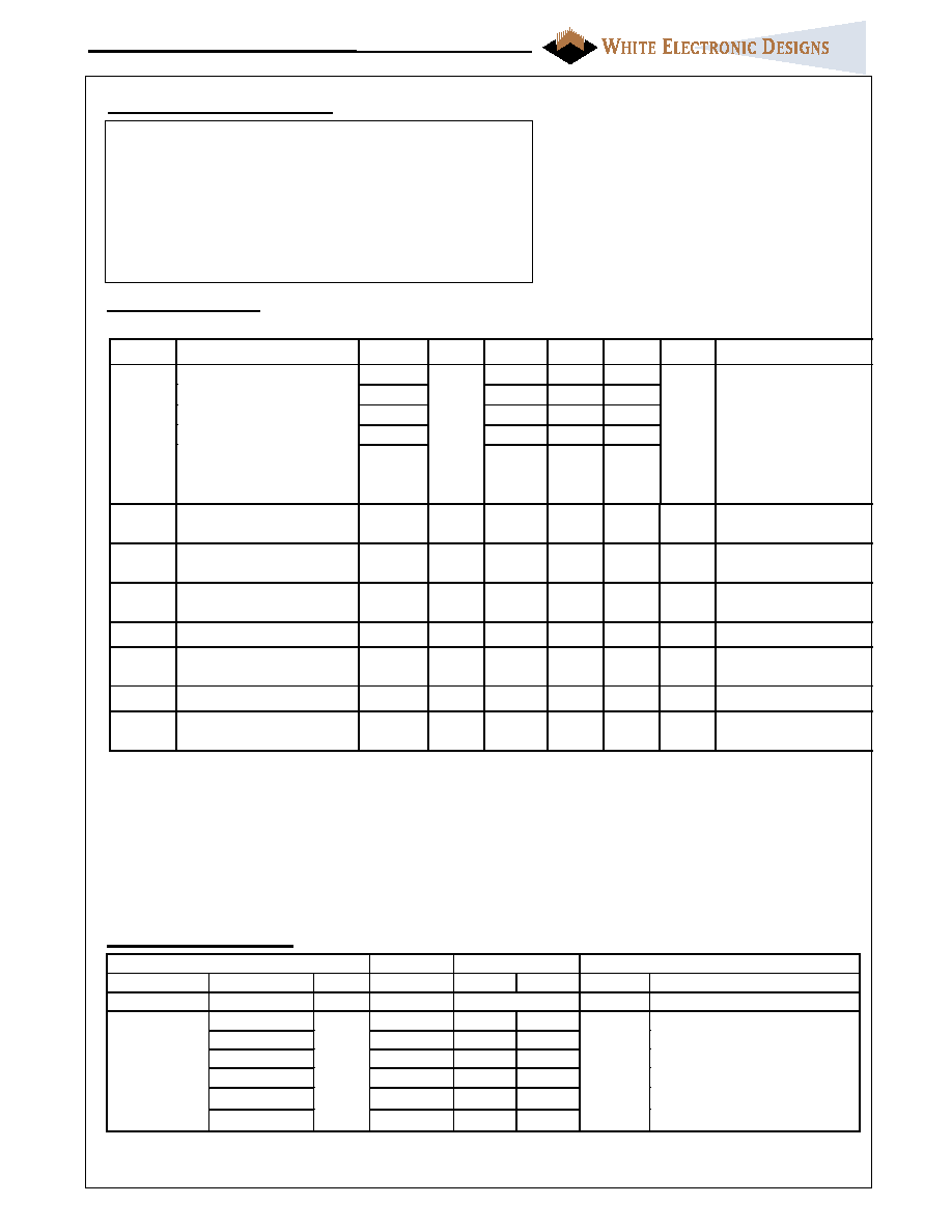
SRAM Memory Card 256KB through 8MB
Block Diagram
4MB SRAM Card Shown
+
decoder
and
control
logic
address
buffer
[A1..A19]
/CSLi
/CSHi
/CSHi
[DO..D7]
[D8..D15]
Write Prot
Switch
S1
WP
Vcc
[A20..A22]
ATTRIBUTE
MEMORY
CE1#
CE2#
WE#
OE#
REG#
+ + +
/CS-A
/CS-A
/RD
/RD
/RD
/WR
/WR
/WR
CTRL
CTRL
A0
Power Management
and
Battery Control
Lithium Bat.
to internal
power
supply
Vcc
BVD1
BVD2
GND
VS1
VS2
[D8..D15]
[DO..D7]
I/O BUFFER
SRAM
512K x 8
[A1..A11]
GND
NC
+
2. pull up resistor (min 10k)
Notes: 1. pull down resistor (min 100k)
+
+
SRAM
512K x 8
SRAM
512K x 8
SRAM
512K x 8
SRAM
512K x 8
SRAM
512K x 8
SRAM
512K x 8
SRAM
512K x 8
General Description
June 2000 Rev. 1 - ECO #12896
2
PCMCIA Flash Memory Card
SRV Series
PC Card Products
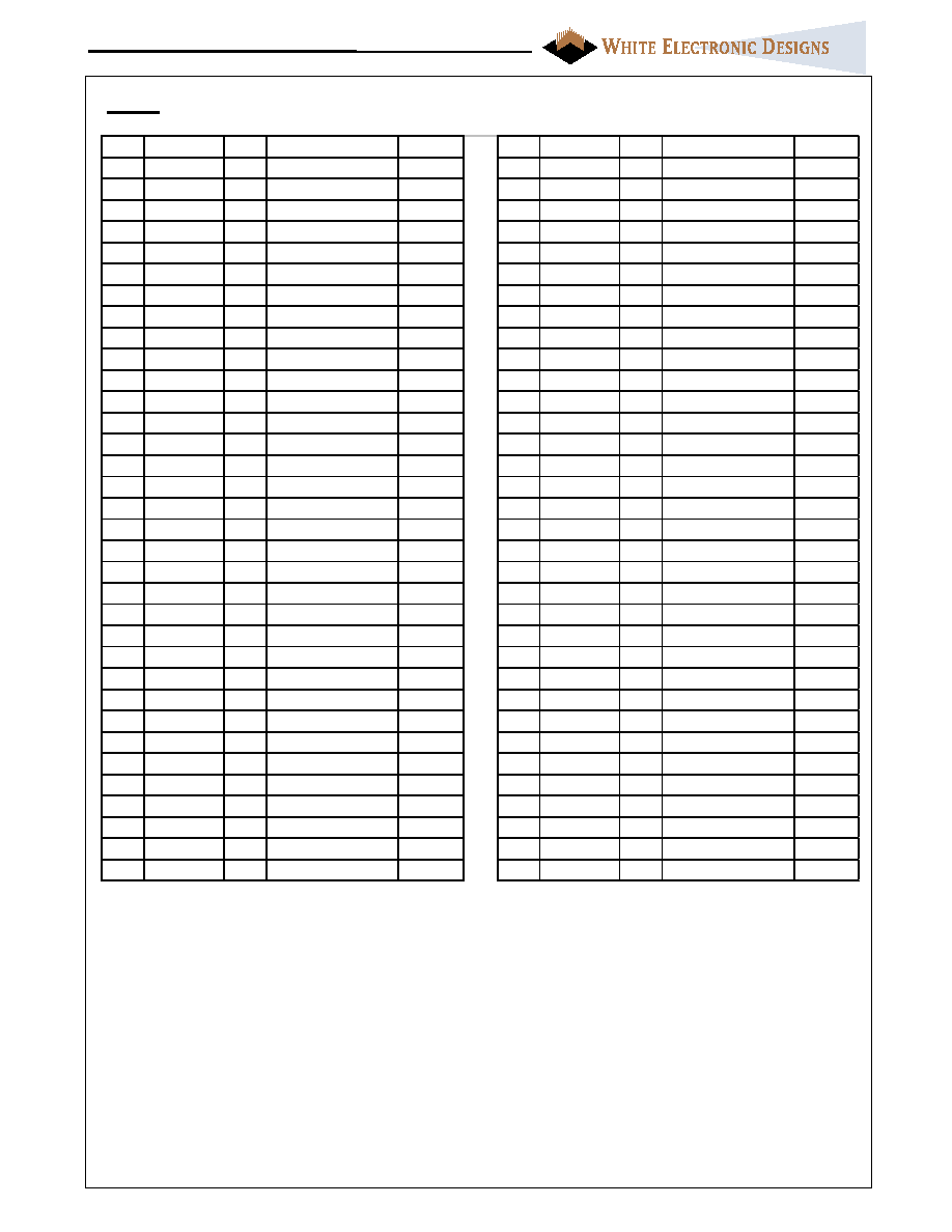
Pinout
Notes:
1. CD1# and CD2# are grounded internal to PC Card.
2. Shows density for which specified address bit is MSB. Higher order address bits are no
connects (ie 1MB A19 is MSB, A20 - A21 are NC).
3. BVD1 is an open drain output with a 10K ohm internal pull-up resistor.
4. The A22 Address line for 8MB capacities is also used for 6MB cards.
Pin Signal name I/O
Function
Active
Pin Signal name I/O
Function
Active
1
GND
Ground
35
GND
Ground
2
DQ3
I/O
Data bit 3
36
CD1#
O
Card Detect 1
LOW
3
DQ4
I/O
Data bit 4
37
DQ11
I/O
Data bit 11
4
DQ5
I/O
Data bit 5
38
DQ12
I/O
Data bit 12
5
DQ6
I/O
Data bit 6
39
DQ13
I/O
Data bit 13
6
DQ7
I/O
Data bit 7
40
DQ14
I/O
Data bit 14
7
CE1#
I
Card enable 1
LOW
41
DQ15
I
Data bit 15
8
A10
I
Address bit 10
42
CE2#
I
Card Enable 2
LOW
9
OE#
I
Output enable
LOW
43
VS1
O
Voltage Sense 1
GND
10
A11
I
Address bit 11
44
N.C.
11
A9
I
Address bit 9
45
N.C.
12
A8
I
Address bit 8
46
A17
I
Address bit 17
256KB(2)
13
A13
I
Address bit 13
47
A18
I
Address bit 18
512KB(2)
14
A14
I
Address bit 14
48
A19
I
Address bit 19
1MB(2)
15
WE#
I
Write Enable
LOW
49
A20
I
Address bit 20
2MB(2)
16 RDY/BSY# O
Ready/Busy
N.C.
50
A21
I
Address bit 21
4MB(2)
17
Vcc
Supply Voltage
51
Vcc
Supply Voltage
18
Vpp1
Prog. Voltage
N.C.
52
Vpp2
Prog. Voltage
N.C.
19
A16
I
Address bit 16
53
A22
Address bit 22
8MB(2,4)
20
A15
I
Address bit 15
54
A23
N.C.
21
A12
I
Address bit 12
55
A24
N.C.
22
A7
I
Address bit 7
56
A25
N.C.
23
A6
I
Address bit 6
57
VS2
O
Voltage Sense 2
N.C.
24
A5
I
Address bit 5
58
N.C.
25
A4
I
Address bit 4
59
Wait#
O
Extended Bus Cycle
Low
26
A3
I
Address bit 3
60
N.C.
27
A2
I
Address bit 2
61
REG#
I
Attrib Mem Select
Low
28
A1
I
Address bit 1
62
BVD2
O
Bat. Volt. Detect 2
29
A0
I
Address bit 0
63
BVD1
O
Bat. Volt. Detect 1
(3)
30
DQ0
I/O
Data bit 0
64
DQ8
I/O
Data bit 8
31
DQ1
I/O
Data bit 1
65
DQ9
I/O
Data bit 9
32
DQ2
I/O
Data bit 2
66
DQ10
O
Data bit 10
33
WP
O
Write Potect
HIGH
67
CD2#
O
Card Detect 2
LOW
34
GND
Ground
68
GND
Ground
June 2000 Rev. 1 - ECO #12896
3
PCMCIA Flash Memory Card
SRV Series
PC Card Products
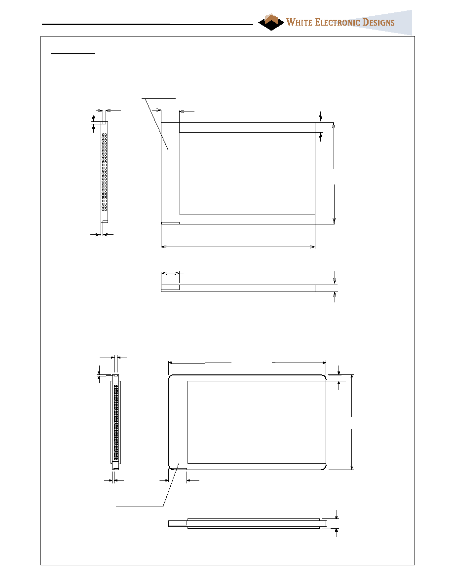
Mechanical
54.0mm
±
0.10
(2.126")
10.0mm MIN
(0.400")
1.6mm
±
0.05
(0.063")
1.0mm
±
0.05
(0.039")
1.0mm
±
0.05
(0.039")
3.3mm
±
T1 (0.130")
T1=0.10mm interconnect area
T1=0.20mm substrate area
Interconnect area
10.0mm MIN
(0.400")
3.0mm MIN
85.6mm
±
0.20
(3.370")
Substrate area
MIN.
1.6mm
±
0.05
0.063"
10.0mm MIN
0.400"
5.0mm
±
T1
0.197"
1.0mm
±
0.05
0.039'
85.6mm
±
0.20
3.370"
3.0mm
54.0mm
±
0.10
2.126"
1.0mm
±
0.05
0.039'
Substrate area
Interconnect area
Type II
Type I
June 2000 Rev. 1 - ECO #12896
4
PCMCIA Flash Memory Card
SRV Series
PC Card Products
Symbol
Type
Name and Function
A0 - A25
INPUT
ADDRESS INPUTS: A0 through A25 enable direct addressing of up
to 64MB of memory on the card. Signal A0 is not used in word access
mode. A25 is the most significant bit. (address pins used are based on
card density,see pinout for highest used address pin)
DQ0 - DQ15
INPUT/OUT
PUT
DATA INPUT/OUTPUT: DQ0 THROUGH DQ15 constitute the
bi-directional databus. DQ0 - DQ7 constitute the lower (even) byte and
DQ8 - DQ15 the upper (odd) byte. DQ15 is the MSB.
CE1#, C E2 #
INPUT
CARD ENA BLE 1 AND 2: CE1# enables even byte accesses, C E2 #
enables odd byte accesses. Multiplexing A0, C E1# and C E2 # allows 8-
bit hosts to access all data on DQ0 - DQ7.
OE#
INPUT
OUTPUT ENA BLE: Active low signal enabling read data from the
memory card.
WE#
INPUT
WRITE ENA BLE: Active low signal gating write data to the memory
card.
RDY/BSY #
OUTPUT
READY/BUSY OUTPUT: Not used for SRAM cards
CD1#, CD2 #
OUTPUT
CARD DETEC T 1 and 2: Provide card insertion detection. These
signals are connected to ground internally on the memory card. The
host socket interface circuitry shall supply 10K-ohm or larger pull-up
resistors on these signal pins.
WP
OUTPUT
WRITE PROTEC T: Follows hardware Write Protect Switch. When
Switch is placed in on position, signal is pulled high (10K ohm). When
switch is off signal is pulled low.
VPP1, VPP2
N.C.
PROGRAM/ERASE POW ER SUPPLY: Not used for SRAM
cards.
VCC
CARD POW ER SUPPLY: 3.3V / 5.0V for all internal circuitry.
GND
GROUND: for all internal circuitry.
REG #
INPUT
ATTRIBUTE MEMORY SELEC T : only used with cards built with
optional attribute memory.
RST
INPUT
RESET: Not used for SRAM cards
WAIT #
OUTPUT
WAIT: This signal is pulled high internally for compatibility. No wait
states are generated.
BVD1, BVD2
OUTPUT
BA TTERY VOLTAG E DETEC T: Provides status of Battery
voltage.
BVD2 = BVD1 = Voh (battery voltage is guaranteed to retain data)
BVD2 = Vol, BVD1 = Voh (data is valid, battery recharge required)
BVD2 = BVD1 = Vol (data may no longer be valid, battery requires
extended recharge)
VS1, VS2
OUTPUT
VOLTAG E SENSE: Notifies the host socket of the card's VCC
requirements. VS1is grounded and VS2 is open to indicate a 3.3V/5V
16 bit card, with a 5V key, has been inserted.
RFU
RESERV ED FOR FUTURE USE
N.C.
NO INTERNA L CONNECTION TO CARD: pin may be driven
or left floating
Card Signal Description
SRAM
FUNCTIONAL TRUTH TABLE
READ function
Common Memory
Attribute Memory
Function Mode
/CE2 /CE1
A0
/OE
/WE
/REG D15-D8
D7-D0
/REG D15-D8
D7-D0
Standby Mode
H
H
X
X
X
X
High-Z
High-Z
X
High-Z
High-Z
Byte Access (8 bits)
H
L
L
L
H
H
High-Z
Even-Byte
L
High-Z
Even-Byte
H
L
H
L
H
H
High-Z
Odd-Byte
L
High-Z
Not Valid
Word Access (16 bits)
L
L
X
L
H
H
Odd-Byte Even-Byte
L
Not Valid Even-Byte
Odd-Byte Only Access
L
H
X
L
H
H
Odd-Byte
High-Z
L
Not Valid
High-Z
WRITE function
Standby Mode
H
H
X
X
X
X
X
X
X
X
X
Byte Access (8 bits)
H
L
L
H
L
H
X
Even-Byte
L
X
Even-Byte
H
L
H
H
L
H
X
Odd-Byte
L
X
X
June 2000 Rev. 1 - ECO #12896
5
PCMCIA Flash Memory Card
SRV Series
PC Card Products
Absolute Maximum Ratings
(2)
Operating Temperature TA (ambient)
Commercial
0∞C to +60 ∞C
Industrial
-40∞C to +85 ∞C
Storage Temperature
Commercial
0∞C to +60 ∞C
Industrial
-40∞C to +85 ∞C
Voltage on any pin relative to VSS
-0.5V to +5.5V (1)
VCC supply Voltage relative to VSS
-0.5V to +7.0V
Notes:
(1) During transitions, inputs may undershoot to
-2.0V or overshoot to VCC +2.0V for periods less
than 20ns.
(2) Stress greater than those listed under
"Absolute Maximum Ratings" may cause
permanent damage to the device. This is a stress
rating only and functional operation at these or
any other conditions greater than those indicated
in the operational sections of this specification is
not implied. Exposure to absolute maximum rating
conditions for extended periods may affect
reliability.
Sym
Parameter
Density
Notes
Min
Typ
(3)
Max
Units
Test Conditions
64KB
90
180
128KB
90
180
256KB
90
180
512KB
90
180
ICC
VCC Active Current
1MB
to
8MB
1
110
190
mA
VCC = 5.25V
tcycle = 150ns
ICCS
VCC Standby Current
All
2,4
< 0.1
< 1
10
mA
VCC = 5.25V
Control Signals = VCC
ILI
Input Leakage Current
All
5,6
±20
µA
VCC = VCCMAX
Vin =VCC or VSS
ILO
Output Leakage Current
All
6
±20
µA
VCC = VCCMAX
Vout =VCC or VSS
VIL
Input Low Voltage
All
6
0
0.8
V
VIH
Input High Voltage
All
6
3.85
VCC
+0.5
V
VOL
Output Low Voltage
All
6
0.4
V
IOL = 3.2mA
VOH
Output High Voltage
All
6
VCC-
0.4
VCC
V
IOH = -2.0mA
Notes:
1. All currents are for x16 mode and are RMS values unless otherwise specified.
2. Control Signals: CE
1
#, CE
2
#, OE#, WE#, REG#.
3. Typical: VCC = 5V, T = +25C.
4. ICCS includes battery recharge current. Value depends on battery discharge level. ICCS min is specified for fully
charged battery. ICCS typical value is specified for battery discharge to 2.7V. ICCS max is specified for a fully
discharged battery (0V). Battery will recharge to 1.5V in 20 sec.
5. Values are the same for byte and word wide modes for all card densities.
6. Exceptions: Leakage currents on CE1#, CE2#, OE#, REG# and WE# will be < 500 µA when VIN = GND due to
internal pull-up resistors.
CMOS Test Conditions: VIL = VSS ± 0.2V, VIH = 5V ± 0.2V
DC Characteristics
(1)
Battery Characteristics
SRV11-14
SRV01-04
Parameter
Density
Notes
Type I
Type I Type II
Units
Conditions
Battery Life
All
(1)
min 10
min 10
years
Normal operation, T=25C
256KB
-
24
60
512KB, 1MB
32
18
45
2MB
22
12
30
4MB
12
7
17
6MB
12
7
17
Battery
Backup Time
8MB
(2)
-
-
12
months
(typical)
T=25C
Battery backup time is a
calculated value and is not
guaranteed. This should not be
used to schedule battery
recharging.
Notes:
1. Battery Life refers to functional lifetime of battery.
2. Battery backup time is density and temperature dependent.
June 2000 Rev. 1 - ECO #12896
6
PCMCIA Flash Memory Card
SRV Series
PC Card Products
5.0V
3.3V
SYM
(PCMCIA)
Parameter
Min
Max
Min
Max
Unit
t
RC
Read Cycle Time
150
250
ns
t
a
(A)
Address Access Time
150
250
ns
t
a
(CE)
Card Enable Access Time
150
250
ns
t
a
(OE)
Output Enable Access Time
75
125
ns
t
su
(A)
Address Setup Time
20
30
ns
t
su
(CE)
Card Enable Setup Time
0
0
ns
t
h
(A)
Address Hold Time
20
20
ns
t
h
(CE)
Card Enable Hold Time
20
20
ns
t
v
(A)
Output Hold from Address Change
0
0
ns
t
dis
(CE)
Output Disable Time from CE#
75
100
ns
t
dis
(OE)
Output Disable Time from OE#
75
100
ns
t
dis
(CE)
Output Enable Time from CE#
5
5
ns
t
dis
(CE)
Output Enable Time from OE#
5
5
ns
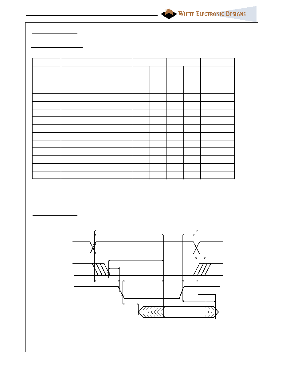
AC Characteristics
Note: AC timing diagrams and characteristics are guaranteed to meet or exceed PCMCIA 2.1 specifications.
Read Timing Diagram
NOTE 1
NOTE 1
A[25::0], /REG
/CE1, /CE2
/OE
D[15::0]
tc(R)
ta(A)
th(A)
tv(A)
ta(CE)
tsu(CE)
th(CE)
ten(OE)
ta(OE)
tsu(A)
DATA VALID
tdis(CE)
tdis(OE)
Note: Signal may be high or low in this area.
Read Timing Parameters
June 2000 Rev. 1 - ECO #12896
7
PCMCIA Flash Memory Card
SRV Series
PC Card Products
5.0V
3.3V
SYM
(PCMCIA)
Parameter
Min
Max
Min
Max
Unit
t
C
W
Write Cycle Time
150
250
ns
t
w
(WE)
Write Pulse Width
80
150
ns
t
su
(A)
Address Setup Time
20
30
ns
t
su
(A-WEH)
Address Setup Time for WE#
100
180
ns
t
su
(CE-WEH)
Card Enable Setup Time for WE#
100
180
ns
t
su
(D-WEH)
Data Setup Time for WE#
50
80
ns
t
h
(D)
Data Hold Time
20
30
ns
t
rec
(WE)
Write Recover Time
20
30
ns
t
dis
(WE)
Output Disable Time from WE#
75
100
ns
t
dis
(OE)
Output Disable Time from OE#
75
100
ns
t
en
(WE)
Output Enable Time from WE#
5
5
ns
t
dis
(OE)
Output Enable Time from OE#
5
5
ns
t
su
(OE-WE)
Output Enable Setup from WE#
10
10
ns
t
h
(OE-WE)
Output Enable Hold from WE#
10
10
ns
t
su
(CE)
Card Enable Setup Time from OE#
0
0
ns
t
h
(CE)
Card Enable Hold Time
20
20
ns
Note: AC timing diagrams and characteristics are guaranteed to meet or exceed PCMCIA 2.1 specifications.
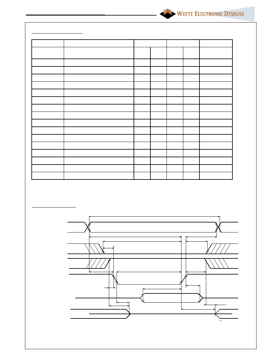
Write Timing Diagram
Write Timing Parameters
th (O E -W E )
N O T E 1
/C E 1 , /C E 2
N O T E 1
ts u (C E -W E H )
tc ( W )
A [2 5 ::0 ], /R E G
tw (W E )
td is (W E )
th (D )
D [1 5 ::0 ](D in )
D A T A IN P U T
ts u (A )
ts u (A -W E H )
/O E
ts u (C E )
ts u ( D -W E H )
tre c (W E )
th (C E )
ts u (O E - W E )
td is (O E )
D [1 5 ::0 ](D o u t)
te n (O E )
te n ( W E )
N O T E 2
N O T E 2
/W E
Notes:
1. Signal may be high or low in this area.
2. When the data I/O pins are in the output state, no signals shall be applied to the data pins (D15 - D0) by the host
system.
June 2000 Rev. 1 - ECO #12896
8
PCMCIA Flash Memory Card
SRV Series
PC Card Products
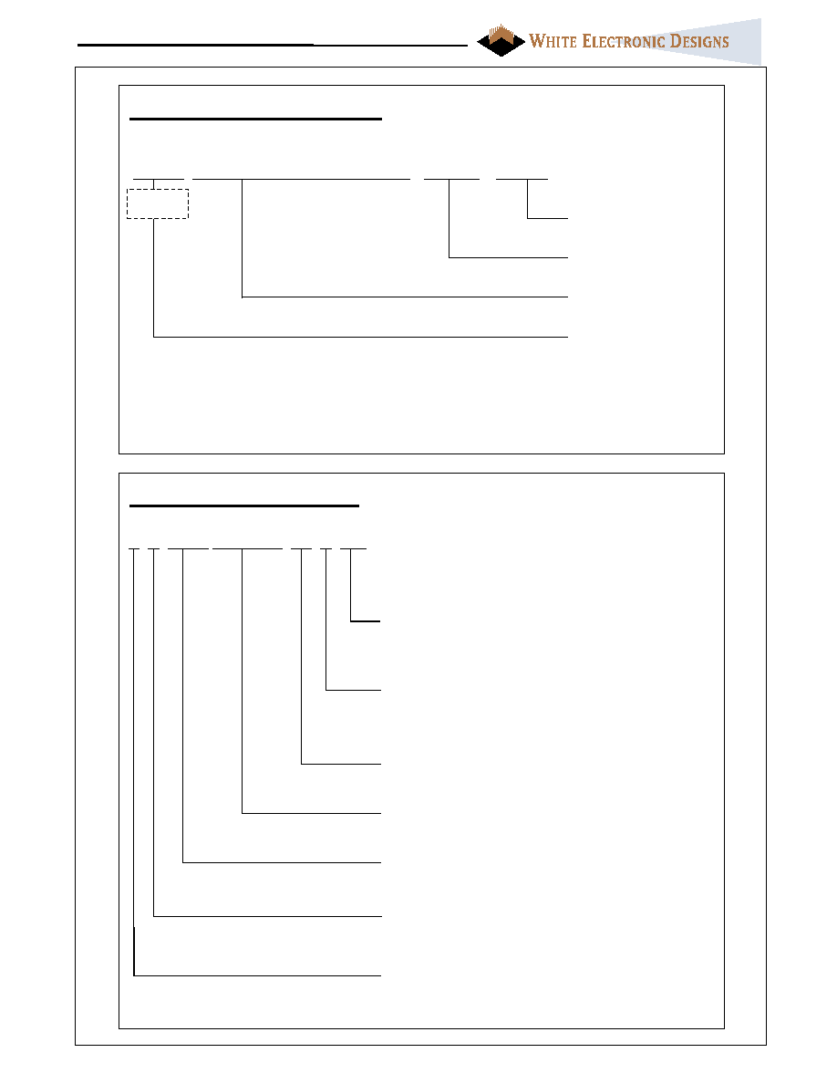
EDI
Company Name
Lot code / trace number
Date code
Part number
PRODUCT MARKING
WED
8P512SRV0100C15 C995 9915
Note:
Some products are currently marked with our pre-merger company name/acronym (EDI). During our
transition period, some products will also be marked with our new company name/acronym (WED).
Starting October 2000 all PCMCIA products will be marked only with the WED prefix.
Card capacity
512 512KB
Packaging option
00
Standard, type 1
PC card
P
Standard PCMCIA
R
Ruggedized PCMCIA
Card family and version
- See Card Family and Version Info. for details (next page)
Temperature range
C Commercial 0∞C to +70∞C
I Industrial -40∞C to +85∞C
Card access time
15
150ns
25
250ns
Card technology
7
FLASH
8
SRAM
PART NUMBERING
8
P
512
SRV01
00
C
15
June 2000 Rev. 1 - ECO #12896
9
PCMCIA Flash Memory Card
SRV Series
PC Card Products
8P XXX SRV YY SS T ZZ
where
XXX:
256
*
256KB
512
*
512KB
001
1MB
002
2MB
004
4MB
006
6MB
008
*
8MB
*
= Capacities available only in SRV01-SRV04
YY:
01
no attribute memory, no Write Protect Switch
02
with attribute memory, no Write Protect Switch
03
with Write Protect Switch, no attribute memory
04
with attribute memory, with Write Protect Switch
11
Extended Battery Backup Time, no attribute memory, no Write Protect Switch
12
Extended Battery Backup Time, with attribute memory, no Write Protect Switch
13
Extended Battery Backup Time, with Write Protect Switch, no attribute memory
14
Extended Battery Backup Time, with attribute memory, with Write Protect Switch
SS:
00
WEDC SRAM Logo Type I
01
Blank Housing,
Type I
02
Blank Housing,
Type I Recessed
03
WEDC SRAM Logo, Type II
(8MB and extended battery backup time)
04
Blank Housing,
Type II
(8MB and extended battery backup time)
05
Blank Housing,
Type II Recessed (8MB and extended battery backup time)
T:
C
Commercial
I
Industrial
ZZ:
15
150ns
Ordering Information
June 2000 Rev. 1 - ECO #12896
10
PCMCIA Flash Memory Card
SRV Series
PC Card Products
Date of revision
Version
Description
27-Sep-99
0
Initial release
2-Jun-00
1
Added Page 8, Added SRV11-14 to page
9, Changed Page Header
REVISION HISTORY
Filename: SRV Dsht Rev1.ppt
White Electronic Designs Corporation
One Research Drive, Westborough, MA 01581, USA
tel:
(508) 366 5151
fax: (508) 836 4850
www.whiteedc.com