1
White Electronic Designs Corporation ∑ (602) 437-1520 ∑ www.wedc.com
White Electronic Designs
WED2ZLRSP01S
April, 2002
Rev. 0
White Electronic Designs Corp. reserves the right to change products or specifi cations without notice.
The WED2ZLRSP01S, Dual Independent Array, NBL-
SSRAM device employs high-speed, Low-Power CMOS
silicon and is fabricated using an advanced CMOS process.
WEDC's 24Mb, Sync Burst SRAM MCP integrates two
totally independent arrays, the fi rst organized as a 512K x
32, and the second a 256K x 32.
All Synchronous inputs pass through registers controlled
by a positive edge triggered, single clock input per array.
The NBL or No Bus Latency Memory provides 100% bus
utilizaton, with no loss of cycles caused by change in modal
operation (Write to Read/Read to Write). All inputs except
for Asynchronous Output Enable and Burst Mode control
are synchronized on the positive or rising edge of Clock.
Burst order control must be tied either HIGH or LOW, Write
cycles are internally self-timed, and writes are initiated on
the rising edge of clock. This feature eliminates the need
for complex off-chip write pulse generation and proved
increased timing fl exibility for incoming signals.
512K x 32/256K x 32 Dual Array
Synchronous Pipeline Burst NBL SRAM
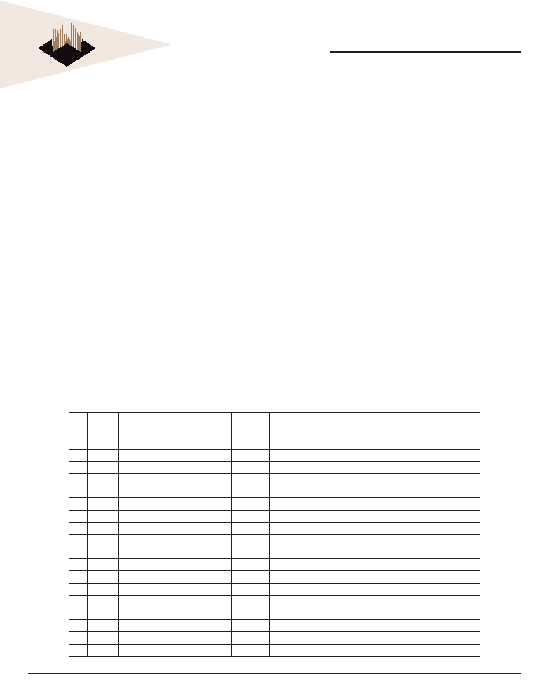
PIN CONFIGURATION
(TOP VIEW)
Fast clock speed: 166, 150, 133, and 100MHz
Fast access times: 3.5ns, 3.8ns, 4.2ns, and 5.0ns
Fast OE# access times: 3.5ns, 3.8ns, 4.2ns, and
5.0ns
Single +2.5V ± 5% power supply (V
CC
)
Snooze Mode for reduced-standby power
Individual Byte Write control
Clock-controlled and registered addresses, data
I/Os and control signals
Burst control (interleaved or linear burst)
Packaging:
209-bump BGA package
Low capacitive bus loading
1
2
3
4
5
6
7
8
9
10
11
A
Vss
A_DATb
0
A_DATb
1
A_DATb
2
A_DATb
3
Vss
A_DATa
0
A_DATa
1
A_DATa
2
A_DATa
3
Vss
B
NC
A_DATb
4
A_DATb
5
A_DATb
6
A_DATb
7
Vss
A_DATa
4
A_DATa
5
A_DATa
6
A_DATa
7
NC
C
A_ADR
A_ADR
A_OE#
A_ADV
A_BWEb
Vss
A_BWEa
A_ZZ
A_ADR
A_ADR
A_ADR
D
A_ADR
Vss
A_CKE#
Vcc
Vcc
Vcc
Vcc
Vcc
Vcc
A_ADR
A_ADR
E
A_ADR
A_CK
A_GWE#
Vcc
Vcc
Vcc
Vcc
Vcc
Vcc
A_ADR
1
A_ADR
0
F
A_ADR
Vss
A_CS
2
#
Vcc
Vcc
Vcc
Vcc
Vcc
Vcc
A_ADR
A_ADR
G
A_ADR
A_ADR
A_CS
1
#
A_CS
2
A_BWEc
Vss
A_BWEd
A_LBO#
A_ADR
A_ADR
A_ADR
H
NC
A_DATc
0
A_DATc
1
A_DATc
2
A_DATc
3
Vss
A_DATd
0
A_DATd
1
A_DATd
2
A_DATd
3
NC
J
Vss
A_DATc
4
A_DATc
5
A_DATc
6
A_DATc
7
Vss
A_DATd
4
A_DATd
5
A_DATd
6
A_DATd
7
Vss
K
Vss
Vss
Vss
Vss
Vss
Vss
Vss
Vss
Vss
Vss
Vss
L
Vss
B_DATb
0
B_DATb
1
B_DATb
2
B_DAT
3
Vss
B_DATa
0
B_DATa
1
B_DATa
2
B_DATa
3
Vss
M
NC
B_DATb
4
B_DATb
5
B_DATb
6
B_DAT
7
Vss
B_DATa
4
B_DATa
5
B_DATa
6
B_DATa
7
NC
N
B_ADR
B_ADR
B_OE#
B_ADV
B_BWEb
Vss
B_BWEa
B_ZZ
B_ADR
B_ADR
B_ADR
P
B_ADR
Vss
B_CKE#
Vcc
Vcc
Vcc
Vcc
Vcc
Vcc
B_ADR
B_ADR
R
B_ADR
B_CK
B_GWE#
Vcc
Vcc
Vcc
Vcc
Vcc
Vcc
B_ADR
1
B_ADR
0
T
B_ADR
Vss
B_CS
2
#
Vcc
Vcc
Vcc
Vcc
Vcc
Vcc
B_ADR
B_ADR
U
B_ADR
NC
B_CS
1
#
B_CS
2
B_BWE
c
Vss
B_BWEd
B_LBO#
B_ADR
B_ADR
B_ADR
V
NC
B_DATc
4
B_DATc
5
B_DATc
6
B_DATc
7
Vss
B_DATd
4
B_DATd
5
B_DATd
6
B_DATd
7
NC
W
Vss
B_DATc
0
B_DATc
1
B_DATc
2
B_DATc
3
Vss
B_DATd
0
B_DATd
1
B_DATd
2
B_DATd
3
Vss
FEATURES
DESCRIPTION
2
White Electronic Designs Corporation ∑ (602) 437-1520 ∑ www.wedc.com
White Electronic Designs
WED2ZLRSP01S
April, 2002
Rev. 0
White Electronic Designs Corp. reserves the right to change products or specifi cations without notice.
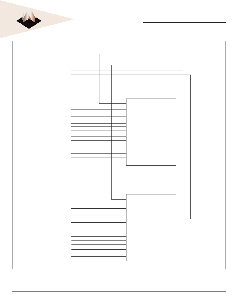
A_SA0-18
B_SA0-17
A_DQ0-31
B_DQ0-31
A_LBO#
A_ZZ
A_ADV
A_OE#
A_CKE#
A_WE#
A_CK
A_BWA#
A_BWB#
A_BWC#
A_BWD#
A_CS2#
A_CS2
A_CS1#
B_LBO#
B_ZZ
B_ADV
B_OE#
B_CKE#
B_WE#
B_CK
B_BWA#
B_BWB#
B_BWC#
B_BWD#
B_CS2#
B_CS2
B_CS1#
LBO#
ZZ
ADV
OE#
CKE#
WE#
CK
BWa#
BWb#
BWc#
BWd#
CS2#
CS2
CS1#
DQ0-31
U1
512K x 32
LBO#
ZZ
ADV
OE#
CKE#
WE#
CK
BWa#
BWb#
BWc#
BWd#
CS2#
CS2
CS1#
DQ0-31
U2
256K x 32
FIG. 1 BLOCK DIAGRAM
3
White Electronic Designs Corporation ∑ (602) 437-1520 ∑ www.wedc.com
White Electronic Designs
WED2ZLRSP01S
April, 2002
Rev. 0
White Electronic Designs Corp. reserves the right to change products or specifi cations without notice.
Write operation occurs when WE# is driven low at the rising
edge of the clock. BW#[d:a] can be used for byte write
operation. The pipe-lined NBL SSRAM uses a late-late write
cycle to utilize 100% of the bandwidth. At the fi rst rising edge
of the clock, WE and address are registered, and the data
associated with that address is required two cycle later.
Subsequent addresses are generated by ADV High for
the burst access as shown below. The starting point of the
burst seguence is provided by the external address. The
burst address counter wraps around to its initial state upon
completion. The burst sequence is determined by the state
of the LBO# pin. When this pin is low, linear burst sequence
is selected. And when this pin is high, Interleaved burst
sequence is selected.
During normal operation, ZZ must be driven low. When ZZ
is driven high, the SRAM will enter a Power Sleep Mode
after 2 cycles. At this time, internal state of the SRAM is
preserved. When ZZ returns to low, the SRAM operates
after 2 cycles of wake up time.
The WED2ZLRSP01S is an NBL Dual Array SSRAM
designed to sustain 100% bus bandwidth by eliminating
turnaround cycle when there is transition from Read to
Write, or vice versa. All inputs (with the exception of OE#,
LBO# and ZZ) are synchronized to rising clock edges,
and all features are available on each of the independent
arrays.
All read, write and deselect cycles are initiated by the
ADV input. Subsequent burst addresses can be internally
generated by the burst advance pin (ADV). ADV should
be driven to Low once the device has been deselected in
order to load a new address for next operation.
Clock Enable (CKE#) pin allows the operation of the chip
to be suspended as long as necessary. When CKE# is
high, all synchronous inputs are ignored and the internal
device registers will hold their previous values. NBL
SSRAM latches external address and initiates a cycle
when CKE# and ADV are driven low at the rising edge
of the clock.
Output Enable (OE#) can be used to disable the output
at any given time. Read operation is initiated when at
the rising edge of the clock, the address presented to
the address inputs are latched in the address register,
CKE# is driven low, the write enable input signals WE#
are driven high, and ADV driven low. The internal array is
read between the fi rst rising edge and the second rising
edge of the clock and the data is latched in the output
register. At the second clock edge the data is driven out
of the SRAM. During read operation OE# must be driven
low for the device to drive out the requested data.
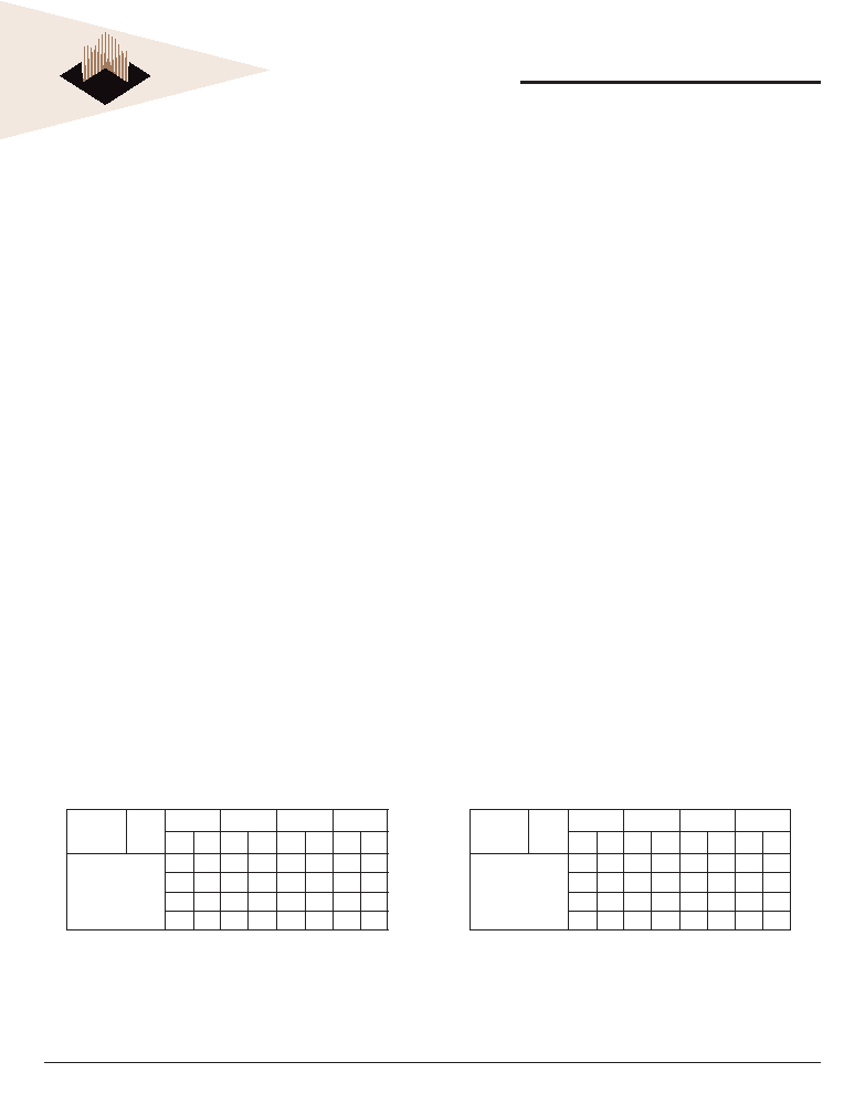
NOTE 1: LBO# pin must be tied to High or Low, and Floating State must not be allowed.
LBO# Pin
High
Case 1
Case 2
Case 3
Case 4
A
1
A
0
A
1
A
0
A
1
A
0
A
1
A
0
First Address
Fourth Address
0
0
0
1
1
0
1
1
0
1
0
0
1
1
1
0
1
0
1
1
0
0
0
1
1
1
1
0
0
1
0
0
BURST SEQUENCE TABLE
FUNCTION DESCRIPTION
(Interleaved Burst, LBO# = High)
(Interleaved Burst, LBO = High)
LBO# Pin
High
Case 1
Case 2
Case 3
Case 4
A
1
A
0
A
1
A
0
A
1
A
0
A
1
A
0
First Address
Fourth Address
0
0
0
1
1
0
1
1
0
1
1
0
1
1
0
0
1
0
1
1
0
0
0
1
1
1
0
0
0
1
1
0
4
White Electronic Designs Corporation ∑ (602) 437-1520 ∑ www.wedc.com
White Electronic Designs
WED2ZLRSP01S
April, 2002
Rev. 0
White Electronic Designs Corp. reserves the right to change products or specifi cations without notice.
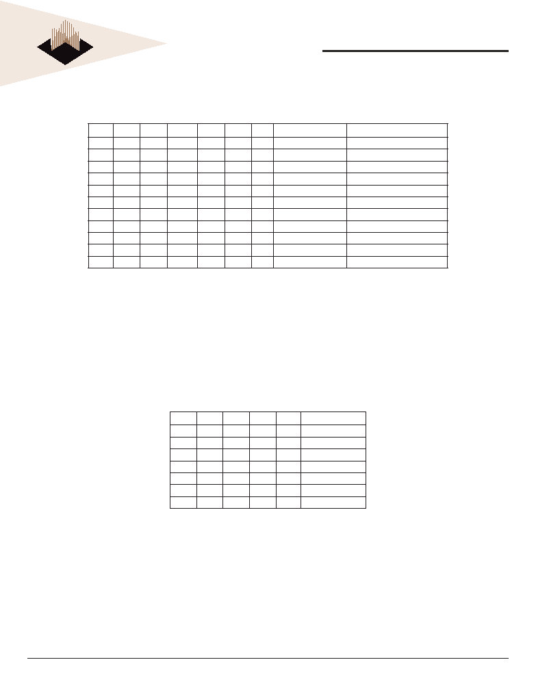
CEx#
ADV
WE#
BWx#
OE#
CKE#
CK
Address Accessed
Operation
H
L
X
X
X
L
N/A
Deselect
X
H
X
X
X
L
N/A
Continue Deselect
L
L
H
X
L
L
External Address
Begin Burst Read Cycle
X
H
X
X
L
L
Next Address
Continue Burst Read Cycle
L
L
H
X
H
L
External Address
NOP/Dummy Read
X
H
X
X
H
L
Next Address
Dummy Read
L
L
L
L
X
L
External Address
Begin Burst Write Cycle
X
H
X
L
X
L
Next Address
Continue Burst Write Cycle
L
L
L
H
X
L
N/A
NOP/Write Abort
X
H
X
H
X
L
Next Address
Write Abort
X
X
X
X
X
H
Current Address
Ignore Clock
TRUTH TABLES
SYNCHRONOUS TRUTH TABLE
WRITE TRUTH TABLE
WE#
BWa# BWb#
BWc# BWd#
Operation
H
X
X
X
X
Read
L
L
H
H
H
Write Byte a
L
H
L
H
H
Write Byte b
L
H
H
L
H
Write Byte c
L
H
H
H
L
Write Byte d
L
L
L
L
L
Write All Bytes
L
H
H
H
H
Write Abort/NOP
NOTES:
1. X means "Don't Care."
2. All inputs in this table must meet setup and hold time around the rising
edge of CK (
).
3. Applies to each of the independent arrays.
NOTES:
1. X means "Don't Care."
2. The rising edge of clock is symbolized by (
)
3. A continue deselect cycle can only be entered if a deselect cycle is executed fi rst.
4. WRITE# = L means Write operation in WRITE TRUTH TABLE.
WRITE# = H means Read operation in WRITE TRUTH TABLE.
5. Operation fi nally depends on status of asynchronous input pins (ZZ and OE#).
6. CEx# refers to the combination of CE
1
#, CE
2
and CE
2
#.
7. Applies to each of the independent arrays.
5
White Electronic Designs Corporation ∑ (602) 437-1520 ∑ www.wedc.com
White Electronic Designs
WED2ZLRSP01S
April, 2002
Rev. 0
White Electronic Designs Corp. reserves the right to change products or specifi cations without notice.
ABSOLUTE MAXIMUM RATINGS*
Voltage on Vdd Supply Relative to V
SS
-0.3V to +3.6V
V
IN
(DQx)
-0.3V to +3.6V
V
IN
(Inputs)
-0.3V to +3.6V
Storage Temperature (BGA)
-55∞C to +125∞C
Short Circuit Output Current
100mA
ELECTRICAL CHARACTERISTICS (0∞C T
A
70∞C)
*Stress greater than those listed under "Absolute Maximum Ratings": may cause permanent damage to the device. This is a stress rating
only and functional operation of the device at these or any other conditions greater than those indicated in the operational sections of this
specifi cation is not implied. Exposure to absolute maximum rating condtions for extended periods may affect reliability.
Description
Symbol
Conditions
Min
Max
Units
Notes
Input High (Logic 1) Voltage
V
IH
1.7
V
CC
+0.3
V
1
Input Low (Logic 0) Voltage
V
IL
-0.3
0.7
V
1
Input Leakage Current
I
LI
0V V
IN
V
CC
-5
5
µA
2
Output Leakage Current
I
LO
Output(s) Disabled, 0V V
IN
V
CC
-5
5
µA
Output High Voltage
V
OH
I
OH
= -1.0mA
2.0
---
V
1
Output Low Voltage
V
OL
I
OL
= 1.0mA
---
0.4
V
1
Supply Voltage
V
CC
2.375
2.625
V
1
NOTES:
1. All voltages referenced to V
SS
(GND)
2. ZZ pin has an internal pull-up, and input leakage is higher.
DC CHARACTERISTICS
NOTES:
1. I
DD
is specifi ed with no output current and increases with faster cycle times. I
DD
increases with faster cycle times and greater output loading.
2. Typical values are measured at 2.5V, 25∞C, and 10ns cycle time.
BGA CAPACITANCE
NOTES:
1. This parameter is sampled.
Description
Symbol
Conditions
Typ
Max
Units
Notes
Control Input Capacitance
C
I
T
A
= 25∞C; f = 1MH
Z
5
7
pF
1
Input/Output Capacitance (DQ)
C
O
T
A
= 25∞C; f = 1MH
Z
6
8
pF
1
Address Capacitance
C
A
T
A
= 25∞C; f = 1MH
Z
5
7
pF
1
Clock Capacitance
C
CK
T
A
= 25∞C; f = 1MH
Z
3
5
pF
1
Description
Symbol
Conditions
Typ
166
MHz
150
MHz
133
MHz
100
MHz
Units
Notes
Power Supply
Current: Operating
I
DD
Device Selected; All Inputs V
IL
or V
IH
; Cycle
Time = t
CYC
MIN; V
CC
= MAX; Output Open
650
600
560
500
mA
1, 2
Power Supply
Current: Standby
I
SB2
Device Deselected; V
CC
= MAX; All Inputs V
SS
+ 0.2
or V
CC
- 0.2; All Inputs Static; CK Frequency = 0;
ZZ V
IL
30
60
60
60
60
mA
2
Power Supply
Current: Current
I
SB3
Device Selected; All Inputs V
IL
or V
IH
; Cycle
Time =t
CYC
MIN; V
CC
= MAX; Output Open;
ZZ V
CC
- 0.2V
20
40
40
40
40
mA
2
Clock Running
Standby Current
I
SB4
Device Deselected; V
CC
= MAX; All Inputs
V
SS
+ 0.2 or V
CC
- 0.2; Cycle Time = t
CYC
MIN; ZZ V
IL
140
120
100
80
mA
2
6
White Electronic Designs Corporation ∑ (602) 437-1520 ∑ www.wedc.com
White Electronic Designs
WED2ZLRSP01S
April, 2002
Rev. 0
White Electronic Designs Corp. reserves the right to change products or specifi cations without notice.
AC CHARACTERISTICS
NOTES:
1. All Address inputs must meet the specifi ed setup and hold times for all rising clock (CK) edges when ADV is sampled low and CEx# is
sampled valid. All other synchronous inputs must meet the specifi ed setup and hold times whenever this device is chip selected.
2. Chip enable must be valid at each rising edge of CK (when ADV is Low) to remain enabled.
3. A write cycle is defi ned by WE# low having been registered into the device at ADV Low. A Read cycle is defi ned by WE# High with ADV Low.
Both cases must meet setup and hold times.
4. Applies to each of the independent arrays.
OUTPUT LOAD (A)
OUTPUT LOAD (B)
(for t
LZC
, t
LZOE
, t
HZOE
, and t
HZC
)
Parameter
Symbol
166MHz
150MHz
133MHz
100MHz
Units
Min
Max
Min
Max
Min
Max
Min
Max
Clock Time
t
CYC
6.0
6.7
7.5
10.0
ns
Clock Access Time
t
CD
--
3.5
--
3.8
--
4.2
--
5.0
ns
Output enable to Data Valid
t
OE
--
3.5
--
3.8
--
4.2
--
5.0 ns
Clock High to Output Low-Z
t
LZC
1.5
--
1.5
--
1.5
--
1.5
--
ns
Output Hold from Clock High
t
OH
1.5
--
1.5
--
1.5
--
1.5
--
ns
Output Enable Low to output Low-Z
t
LZOE
0.0
--
0.0
--
0.0
--
0.0
--
ns
Output Enable High to Output High-Z
t
HZOE
--
3.0
--
3.0
--
3.5
--
3.5 ns
Clock High to Output High-Z
t
HZC
--
3.0
--
3.0
--
3.5
--
3.5 ns
Clock High Pulse Width
t
CH
2.2
--
2.5
--
3.0
--
3.0
--
ns
Clock Low Pulse Width
t
CL
2.2
--
2.5
--
3.0
--
3.0
--
ns
Address Setup to Clock High
t
AS
1.5
--
1.5
--
1.5
--
1.5
--
ns
CKE# Setup to Clock High
t
CES
1.5
--
1.5
--
1.5
--
1.5
--
ns
Data Setup to Clock High
t
DS
1.5
--
1.5
--
1.5
--
1.5
--
ns
Write Setup to Clock High
t
WS
1.5
--
1.5
--
1.5
--
1.5
--
ns
Address Advance to Clock High
t
ADVS
1.5 1.5 1.5 1.5 ns
Chip Select Setup to Clock High
t
CSS
1.5 1.5 1.5 1.5 ns
Address Hold to Clock high
t
AH
0.5
--
0.5
--
0.5
--
0.5
--
ns
CKE# Hold to Clock High
t
CEH
0.5
--
0.5
--
0.5
--
0.5
--
ns
Data Hold to Clock High
t
DH
0.5
--
0.5
--
0.5
--
0.5
--
ns
Write Hold to Clock High
t
WH
0.5
--
0.5
--
0.5
--
0.5
--
ns
Address Advance to Clock High
t
ADVH
0.5
--
0.5
--
0.5
--
0.5
--
ns
Chip Select Hold to Clock High
t
CSH
0.5
--
0.5
--
0.5
--
0.5
--
ns
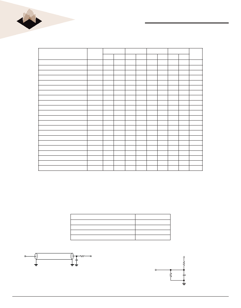
*Including Scope and Jig Capacitance
AC TEST CONDITIONS
(0 T
A
70∞C, V
CC
= 2.5V ± 5%, Unless Otherwise Specifi ed)
Parameter
Value
Input Pulse Level
0 to 2.5V
Input Rise and Fall Time (Measured at 20% to 80%)
1.0V/ns
Input and Output Timing Reference Levels
1.25V
Output Load
See Output Load (A)
Dout
Zo=50
RL=50
VL=1.25V
30pF*
Dout
1538
5pF*
+2.5V
1667
7
White Electronic Designs Corporation ∑ (602) 437-1520 ∑ www.wedc.com
White Electronic Designs
WED2ZLRSP01S
April, 2002
Rev. 0
White Electronic Designs Corp. reserves the right to change products or specifi cations without notice.
SNOOZE MODE is a low-current, "power-down" mode
in which the device is deselected and current is reduced
to I
SB2Z
. The duration of SNOOZE MODE is dictated by
the length of time Z is in a HIGH state. After the device
enters SNOOZE MODE, all inputs except ZZ become
gated inputs and are ignored. ZZ is an asynchronous,
active HIGH input that causes the device to enter
SNOOZE MODE.
When ZZ becomes a logic HIGH, I
SB2Z
is guaranteed after
the setup time t
ZZ
is met. Any READ or WRITE operation
pending when the device enters SNOOZE MODE is not
guaranteed to complete successfully. Therefore, SNOOZE
MODE must not be initiated until valid pending operations
are completed.
SNOOZE MODE
Description Conditions
Symbol
Min
Max
Units
Notes
Current during SNOOZE MODE
ZZ V
IH
I
SB2Z
10 mA
ZZ active to input ignored
t
ZZ
2(t
KC
)
ns
1
ZZ inactive to input sampled
t
RZZ
2(t
KC
)
ns
1
ZZ active to snooze current
t
ZZI
2(t
KC
)
ns
1
ZZ inactive to exit snooze current
t
RZZI
ns 1
FIG. 2 SNOOZE MODE TIMING DIAGRAM
ZZ
I
SUPPLY
CLOCK
ALL INPUTS
(except ZZ)
Output (Q)
t
ZZ
t
ZZI
t
RZZ
t
RZZI
HIGH-Z
DESELECT or READ Only
I
ISB2Z
DON'T CARE
SNOOZE MODE
8
White Electronic Designs Corporation ∑ (602) 437-1520 ∑ www.wedc.com
White Electronic Designs
WED2ZLRSP01S
April, 2002
Rev. 0
White Electronic Designs Corp. reserves the right to change products or specifi cations without notice.
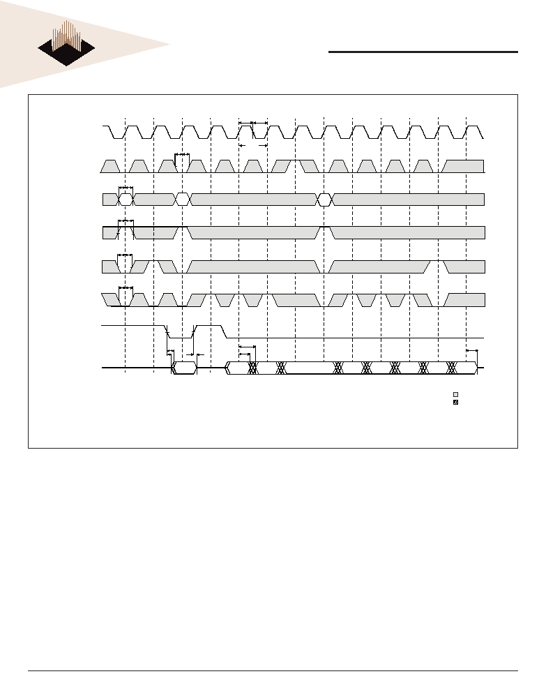
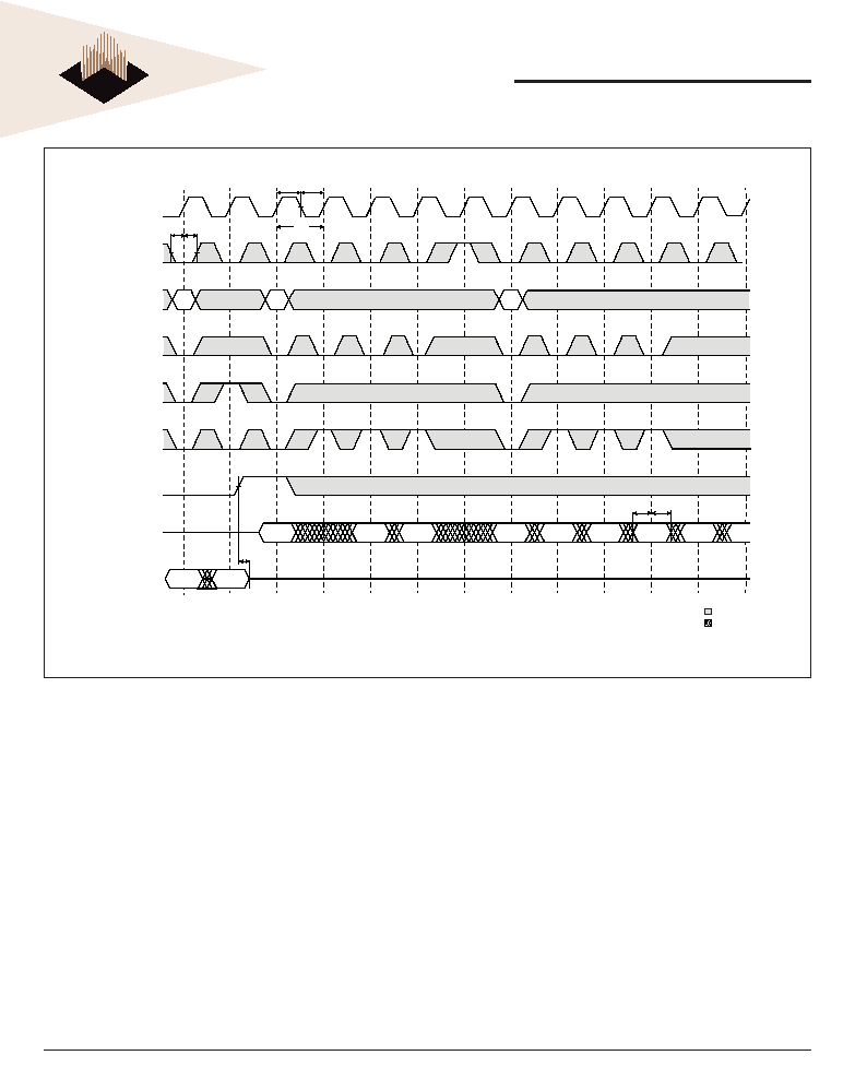
Clock
CKE#
Address
WRITE#
CEx#
ADV
OE#
Data Out
t
CH
t
CL
t
CYC
t
CES
t
CEH
t
AS
t
AH
t
WS
t
WH
t
CSS
t
CSH
t
ADVS
t
ADVH
t
OE
t
LZOE
t
HZOE
t
CD
t
OH
t
HZC
A1
A2
A3
Q1-1
Q2-1
Q2-2
Q2-3
Q2-4
Q3-1
Q3-2
Q3-3
Q3-4
Dont Care
Undefined
NOTES:
WRITE# = L means WE# = L, and BWx# = L
CEx# refers to the combination of CE1#, CE2 and CE2#.
FIG. 3 TIMING WAVEFORM OF READ CYCLE
Note:
Applies to both independent arrays.
9
White Electronic Designs Corporation ∑ (602) 437-1520 ∑ www.wedc.com
White Electronic Designs
WED2ZLRSP01S
April, 2002
Rev. 0
White Electronic Designs Corp. reserves the right to change products or specifi cations without notice.
FIG. 4 TIMING WAVEFORM OF WRITE CYCLE
Clock
CKE#
Address
WRITE#
CEx#
ADV
OE#
Data Out
Data In
t
CH
t
CL
t
CYC
t
CSS
t
CSH
t
HZOE
t
DS
t
DH
A1
A2
A3
D1-1
Q0-4
Q0-3
D2-1
D2-2
D2-3
D2-4
D3-1
D3-2
D3-3
D3-4
Dont Care
Undefined
NOTES:
WRITE# = L means WE# = L, and BWx# = L
CEx# refers to the combination of CE1#, CE2 and CE2#.
Note:
Applies to both independent arrays.
10
White Electronic Designs Corporation ∑ (602) 437-1520 ∑ www.wedc.com
White Electronic Designs
WED2ZLRSP01S
April, 2002
Rev. 0
White Electronic Designs Corp. reserves the right to change products or specifi cations without notice.
FIG. 5 TIMING WAVEFORM OF SINGLE READ/WRITE
Clock
CKE#
Address
WRITE#
CEx#
ADV
OE#
Data Out
Data In
t
CH
t
CL
t
CYC
t
CES
t
CEH
t
LZOE
t
OE
t
DS
t
DH
A1
A2
A3
A4
A5
A6
A7
A8
A9
D2
Q1
Q2
Q4
D5
Q6
Q7
Dont Care
Undefined
NOTES:
WRITE# = L means WE# = L, and BWx# = L
CEx# refers to the combination of CE1#, CE2 and CE2#.
Note:
Applies to both independent arrays.
11
White Electronic Designs Corporation ∑ (602) 437-1520 ∑ www.wedc.com
White Electronic Designs
WED2ZLRSP01S
April, 2002
Rev. 0
White Electronic Designs Corp. reserves the right to change products or specifi cations without notice.
FIG. 6 TIMING WAVEFORM OF CKE# OPERATION
Clock
CKE#
Address
WRITE#
CEx#
ADV
OE#
Data Out
Data In
t
CH
t
CL
t
CYC
t
CES
t
CEH
t
CD
t
LZC
t
HZC
t
DS
t
DH
A1
A2
A3
A4
A5
A6
Q1
Q3
D2
Q4
Dont Care
Undefined
NOTES:
WRITE# = L means WE# = L, and BWx# = L
CEx# refers to the combination of CE1#, CE2 and CE2#.
Note:
Applies to both independent arrays.
12
White Electronic Designs Corporation ∑ (602) 437-1520 ∑ www.wedc.com
White Electronic Designs
WED2ZLRSP01S
April, 2002
Rev. 0
White Electronic Designs Corp. reserves the right to change products or specifi cations without notice.
Clock
CKE#
Address
WRITE#
CEx#
ADV
OE#
Data Out
Data In
t
CH
t
CL
t
CYC
t
CSS
t
CSH
t
LZOE
t
OE
t
HZC
t
DS
t
DH
t
LZC
t
CD
A1
A2
A3
A4
A5
Q1
Q2
D3
Q4
D5
Dont Care
Undefined
NOTES:
WRITE# = L means WE# = L, and BWx# = L
CEx# refers to the combination of CE1#, CE2 and CE2#.
FIG. 7 TIMING WAVEFORM OF CE# OPERATION
Note:
Applies to both independent arrays.
13
White Electronic Designs Corporation ∑ (602) 437-1520 ∑ www.wedc.com
White Electronic Designs
WED2ZLRSP01S
April, 2002
Rev. 0
White Electronic Designs Corp. reserves the right to change products or specifi cations without notice.
Part Number
Confi guration
tCD
(ns)
Clock
(MHz)
Operating
Range
Temperature
Range
WED2ZLRSP01S35BC
512K x 32/256K x 32
3.5
166
Commercial
0∞ - 70∞ C
WED2ZLRSP01S38BC
512K x 32/256K x 32
3.8
150
Commercial
0∞ - 70∞C
WED2ZLRSP01S42BC
512K x 32/256K x 32
4.2
133
Commercial
0∞ - 70∞C
WED2ZLRSP01S50BC
512K x 32/256K x 32
5.0
100
Commercial
0∞ - 70∞C
WED2ZLRSP01S38BI
512K x 32/256K x 32
3.8
150
Industrial
-40∞ - 85∞C
WED2ZLRSP01S42BI
512K x 32/256K x 32
4.2
133
Industrial
-40∞ - 85∞C
WED2ZLRSP01S50BI
512K x 32/256K x 32
5.0
100
Industrial
-40∞ - 85∞C
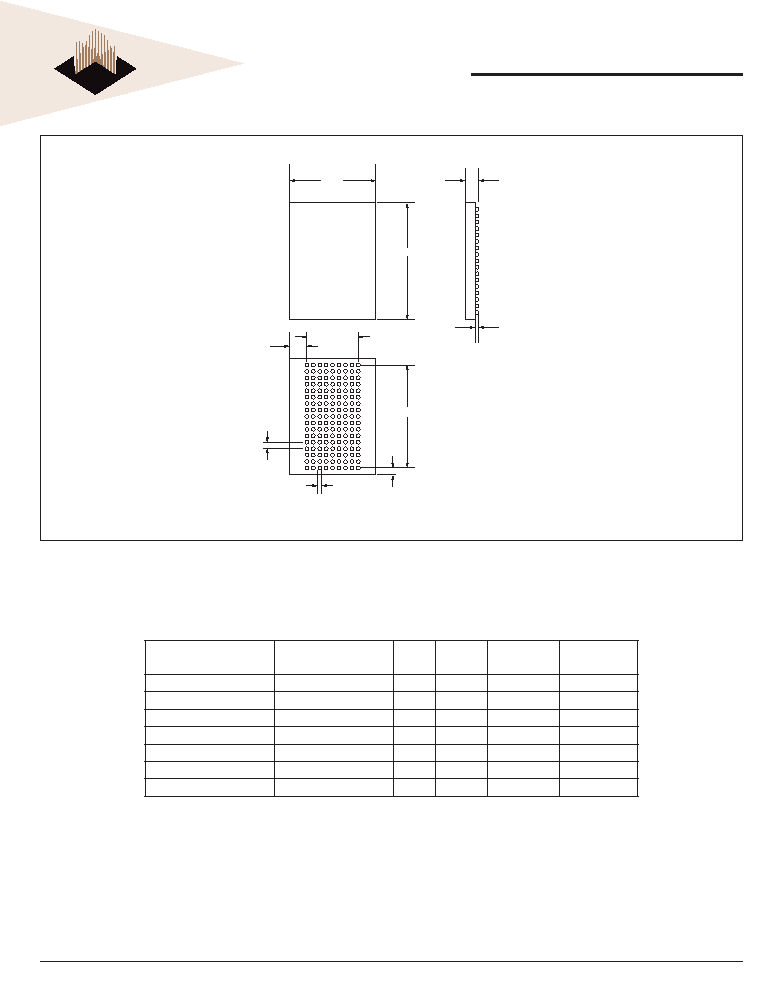
PACKAGE DIMENSION: 153 BUMP PBGA
ALL LINEAR DIMENSIONS ARE IN MILLIMETERS AND PARENTHETICALLY IN INCHES
ORDERING INFORMATION
NOTE: Ball attach pad for above BGA package is 620 microns in diameter. Pad is solder mask defi ned.
17.00
23.00
3.50
10.00
1.00
18.00
2.5
.60 ± .050
0.50 ± 10
2.33 Max
Commercial Temp Range (0∞C to 70∞C)