
WT62P1
Data Sheet Rev. 1.01
Weltrend Semiconductor, Inc.
Page 2
GENERAL DESCRIPTION
The WT62P1 is a microcontroller for digital controlled monitor with Universal Serial Bus (USB) interface.
It contains an 8-bit CPU, 32K bytes flash memory, 512 bytes RAM, 14 PWMs, parallel I/Os, SYNC signal
processor, timer, DDC1/2B interface, master/slave I
2
C interface, low speed USB device module, 6-bit
A/D converter and watch-dog timer.
FEATURES
∑
8-bit 6502 compatible CPU with 6MHz operating frequency
∑
32768 bytes flash memory, 512 bytes SRAM
∑
12MHz crystal oscillator
∑
14 channels 8-bit PWM outputs
∑
Sync signal processor with H+V separation, H/V frequency counter, H/V polarity detection/control and
clamp pulse output
∑
Six free-running sync signal outputs (Horizontal frequency up to 106KHz)
∑
Self-test
pattern
∑
DDC1/2B
supported
∑
Fast mode master/slave I
2
C interface (up to 400KHz)
∑
Embedded USB function with endpoint 0 and endpoint 1
∑
Built-in 3.3V regulator for USB tranceiver
∑
Watch-dog
timer
∑
Maximum 28 programmable I/O pins
∑
One 8-bit programmable timer
∑
6-bit A/D converter with 4 selectable inputs
∑
One external interrupt request input
∑
Low
V
DD
reset
ORDERING INFORMATION
Package Type
Part Number
42-pin PDIP
WT62P1-N42
42-pin Shrink PDIP
WT62P1-K42
40-pin PDIP
WT62P1-N40
28-pin skinny PDIP
WT62P1-N28
44-pin SOP
WT62P1-S44

WT62P1
Data Sheet Rev. 1.01
Weltrend Semiconductor, Inc.
Page 3
PIN CONFIGURATION
44
43
42
41
40
39
38
37
36
35
34
33
32
31
30
29
28
27
26
25
24
23
22
21
1
20
19
18
17
16
15
14
13
12
11
10
9
8
7
6
5
4
3
2
D+
D-
GND
HIN
IRQ
OSCI
OSCO
PA0/SDA1
PA1/SCL1
PA2/PWM8
PA3/PWM9
PA4/PWM10
PA5/PWM11
PA6/PWM12
PA7/PWM13/CLAMP
PB0/HFO
PB1/HFI
PB2
PB3/PAT
PB4/SCL2
PB5/SDA2
PC0/AD0
PC1/AD1
PC2/AD2
PC3/AD3
PC4
PC5
PC6
PC7/SOGIN
PD0/VOUT
PD1/HOUT
PD2/PWM7
PD3/PWM6
PD4/PWM5
PD5/PWM4
PWM0
PWM1
PWM2
PWM3
RESET/3V3
VDD
VIN
15
16
17
18
19
20
21
28
27
26
25
24
23
22
1
14
13
12
11
10
9
8
7
6
5
4
3
2
GND
HIN
IRQ
OSCI
OSCO
PA0/SDA1
PA1/SCL1
PA2/PWM8
PA3/PWM9
PA4/PWM10
PA5/PWM11
PA6/PWM12
PA7/PWM13/CLAMP
PB4/SCL2
PB5/SDA2
PC0/AD0
PC1/AD1
PC2/AD2
PC3/AD3
PC4
PC5
PC6
PC7
PD0/VOUT
PD1/HOUT
RESET/3V3
VDD
VIN
42
41
40
39
38
37
36
35
34
33
32
31
30
29
28
27
26
25
24
23
22
21
1
20
19
18
17
16
15
14
13
12
11
10
9
8
7
6
5
4
3
2
D+
D-
GND
HIN
IRQ
OSCI
OSCO
PA0/SDA1
PA1/SCL1
PA2/PWM8
PA3/PWM9
PA4/PWM10
PA5/PWM11
PA6/PWM12
PA7/PWM13/CLAMP
PB0/HFO
PB1/HFI
PB2
PB3/PAT
PB4/SCL2
PB5/SDA2
PC0/AD0
PC1/AD1
PC2/AD2
PC3/AD3
PC4
PC5
PC6
PC7/SOGIN
PD0/VOUT
PD1/HOUT
PD2/PWM7
PD3/PWM6
PD4/PWM5
PD5/PWM4
PWM0
PWM1
PWM2
PWM3
RESET/3V3
VDD
VIN
21
40
39
38
37
36
35
34
33
32
31
30
29
28
27
26
25
24
23
22
1
20
19
18
17
16
15
14
13
12
11
10
9
8
7
6
5
4
3
2
GND
HIN
IRQ
OSCI
OSCO
PA0/SDA1
PA1/SCL1
PA2/PWM8
PA3/PWM9
PA4/PWM10
PA5/PWM11
PA6/PWM12
PA7/PWM13/CLAMP
PB0/HFO
PB1/HFI
PB2
PB3/PAT
PB4/SCL2
PB5/SDA2
PC0/AD0
PC1/AD1
PC2/AD2
PC3/AD3
PC4
PC5
PC6
PC7/SOGIN
PD0/VOUT
PD1/HOUT
PD2/PWM7
PD3/PWM6
PD4/PWM5
PD5/PWM4
PWM0
PWM1
PWM2
PWM3
RESET/3V3
VDD
VIN
WT62P1-N28
WT62P1-S44
WT62P1-N42
WT62P1-K42
WT62P1-N40
40-pin PDIP
44-pin SOP
28-pin Skinny PDIP
42-pin PDIP
42-pin SPDIP

WT62P1
Data Sheet Rev. 1.01
Weltrend Semiconductor, Inc.
Page 4
PIN DESCRIPTION
Pin No.
44 42 40 28
Pin Name
I/O
Description
1
1
-
- D+
I/O USB D+ signal.
2
2
1
- PWM2
O PWM2 output (10V open-drain).
3
3
2
- PWM1
O PWM1 output (5V open-drain).
4
4
3
- PWM0
O PWM0 output (5V open-drain).
5
5
4
8 /RESET/3V3
I
Reset input and +3.3V regulator output for USB tranceiver power
supply.
6
6
5
9 VDD
+5V power supply.
7
-
-
- NC
No Connection.
8
7
6
10 GND
Ground.
9
8
7
11 OSCO
I/O 12MHz oscillator output.
10
9
8
12 OSCI
I
12MHz oscillator input.
11 10
9
13 PB5/ SDA2
I/O Port B5 or I
2
C interface data line.
12 11 10 14 PB4/ SCL2
I/O Port B4 or I
2
C interface clock line.
13 12 11
- PB3/PAT
I/O Port B3 or test pattern output
14 13 12
- PB2
I/O Port B2.
15 14 13
- PB1/HFI
I/O Port B1 or half frequency divider input.
16 15 14
- PB0/HFO
I/O Port B0 or half frequency divider output.
17 16 15 15 /IRQ
I
Interrupt request input, A low level on this can generate interrupt.
18 17 16 16 PC7/SOGIN
I/O Port C7 or Sync on Green input.
19 18 17 17 PC6
I/O Port C6.
20 19 18 18 PC5
I/O Port C5.
21 20 19 19 PC4
I/O Port C4.
22 21 20 20 PC3/AD3
I/O Port C3 or ADC input 3.
23 22 21 21 PC2/AD2
I/O Port C2 or ADC input 2.
24 23 22 22 PC1/AD1
I/O Port C1 or ADC input 1.
25 24 23 23 PC0/AD0
I/O Port C0 or ADC input 0.
26 25 24 24 PA0/SDA1
I/O Port A0 or DDC interface SDA pin.
27 26 25 25 PA1/SCL1
I/O Port A1 or DDC interface SCL pin.
28 27 26 26 PA2/PWM8
I/O Port A2 or PWM8 output.
29 28 27 27 PA3/PWM9
I/O Port A3 or PWM9 output.
30 29 28 28 PA4/PWM10
I/O Port A4 or PWM10 output.
31 30 29
1 PA5/PWM11
I/O Port A5 or PWM11 output.
32 31 30
2 PA6/PWM12
I/O Port A6 or PWM12 output.
33 32 31
3 PA7/PWM13/
CLAMP
I/O Port A7 or PWM13 output or clamp pulse output.
34 33 32
4 PD0/VOUT
I/O Port D0 or Vsync output.
35 34 33
5 PD1/HOUT
I/O Port D1 or Hsync output.
36 35 34
- PD2/PWM7
I/O Port D2 or PWM7 output.
37 36 35
- PD3/PWM6
I/O Port D3 or PWM6 output.
38
-
-
- NC
No Connection.
39 37 36
- PD4/PWM5
I/O Port D4 or PWM5 output.
40 38 37
- PD5/PWM4
I/O Port D5 or PWM4 output.
41 39 38
- PWM3
I/O PWM3 output (10V open-drain).
42 40 39
6 HIN
I
Hsync Input.
43 41 40
7 VIN
I
Vsync input.
44 42
-
- D-
I/O USB D- signal.

WT62P1
Data Sheet Rev. 1.01
Weltrend Semiconductor, Inc.
Page 5
FUNCTIONAL DESCRIPTION
CPU
8-bit 6502 compatible CPU operates at 6MHz. Address bus is 16-bit and data bus is 8-bit.
The non-maskable interrupt (/NMI) of 6502 is modified to be maskable and is defined as INT0 with higher
priority. The interrupt request (/IRQ) of 6502 is defined as INT1 with lower priority.
Please refer the 6502 reference menu for more detail.
RAM
512 bytes RAM. Address is located from $0080h to $00FFh and $0180h to $02FFh.
RAM from $0200h to $027Fh and $0280h to $02FFh can be disabled individually to emulate different
RAM size IC. (see Register $0FFFh)
ROM
32768 bytes flash memory for program. Address is located from $8000h to $FFFFh.
The following addresses are reserved for special purpose :
$FFFAh (low byte) and $FFFBh (high byte) : INT0 interrupt vector.
$FFFCh (low byte) and $FFFDh (high byte) : program reset interrupt vector.
$FFFEh (low byte) and $FFFFh (high byte) : INT1 interrupt vector.
$0000h
:
$003Fh
Registers
$0040h
:
$007Fh
Reserved
$0080h
:
$00FFh
128 bytes RAM
$0100h
:
$017Fh
Reserved
$0180h
:
$02FFh
384 bytes RAM
$0300h
:
$0FFEh
Reserved
$0FFFh Configuration Register
$1000h
:
$7FFFh
Reserved
$8000h
:
:
:
$FFFFh
Flash ROM
System Reset
There are four reset sources of this controller. Fig.1 shows the block diagram of reset logic.

WT62P1
Data Sheet Rev. 1.01
Weltrend Semiconductor, Inc.
Page 6
Fig. 1 Reset Signals
External Reset
A low level on the RESET/3.3V pin will generate reset.
Illegal address Reset
When the address bus of CPU goes to illegal address, a reset pulse will be generated.
The illegal address is defined as $0040h~$007Fh, $0300h~$0FFEh and $1000h~$7FFFh.
Low VDD Voltage Reset
When VDD is below 3.9V, an internal reset signal is generated. The reset signal will last 2.048 ms after
the voltage is higher than 3.9V.
Watchdog Timer Reset
If a time-out happens when watchdog timer is enabled, a reset pulse is generated. Please refer
watchdog timer section for more information.
�
!"#$�
�
%&'
&
(
%)

WT62P1
Data Sheet Rev. 1.01
Weltrend Semiconductor, Inc.
Page 7
I/O Port
I/O Port A
Pin PA0 and PA1 are shared with DDC interface SDA1 and SCL1 When ENDDC bit is " 0" , These two
pins becomes I/O port. If PA0OE bit is set, Pin PA0 is an open-drain output. If PA0OE is cleared, Pin
PA0 is an input pin with no internal pull-up resistor. The operation of PA1 is same as PA0. Fig. 2 Shows
the structure of PA0.
Fig.2 Structure of PA0 and PA1
Pin PA2 to PA6 are shared with PWM output. When corresponding EPWMx bit is " 0" , the pin is I/O port.
If PAxOE bit is set, it is a push-pull type output. If PAxOE bit is cleared, it is an input pin with internal
pull-up resistor.
Pin PA7 is shared with PWM13 output and clamp pulse output. When both EPWM13 bit and ENCLP bit
are " 0" , this pin becomes I/O port. If PA7OE bit is set, it is a push-pull type output. If PA7OE bit is
cleared, it is an input pin with internal pull-up resistor.
Fig.3 Structure of PA2
C
D
R
Q
QN
C
D
R
Q
QN
INTERNAL_DATA_BUS
DATA[0]
PA0OE
PA0
WRITE_PA_CTRL
RESET
DATA[0]
PA0
WRITE_PA_DATA
RESET
READ_PA_DATA
DATA[0]
C
D
R
Q
QN
C
D
R
Q
QN
INTERNAL_DATA_BUS
DATA[2]
PA2OE
WRITE_PA_CTRL
PA2
RESET
DATA[2]
PA2
WRITE_PA_DATA
RESET
READ_PA_DATA
DATA[2]

WT62P1
Data Sheet Rev. 1.01
Weltrend Semiconductor, Inc.
Page 8
Port A Control Register
Name
Addr R/W Initial
Bit 7
Bit 6
Bit 5
Bit4
Bit 3
Bit 2
Bit 1
Bit 0
PA_CTRL 0000h W
00h
PA7OE
PA6OE
PA5OE
PA4OE
PA3OE
PA2OE
PA1OE
PA0OE
Bit Name
Description
PAnOE
Port An Output Enable.
When it is set, PAn is output pin.
When it is cleared, PAn is input pin with internal pull high (except PA0 and PA1 pins).
Port A Data Register
Name
Addr R/W Initial
Bit 7
Bit 6
Bit 5
Bit4
Bit 3
Bit 2
Bit 1
Bit 0
R
00h
PA7
PA6
PA5
PA4
PA3
PA2
PA1
PA0
PA_DATA 0001h
W
00h
PA7
PA6
PA5
PA4
PA3
PA2
PA1
PA0
Bit Name
Description
PAn (W) This bit controls the output level when the corresponding PAnOE bit is set.
When PAn=1, PAn pin outputs high level. (PA0 and PA1 are open-drain output)
When PAn=0, PAn pin outputs low level.
PAn (R)
When PAnOE=1 (i.e. output port), this bit is same as PAn (W).
When PAnOE=0, this bit indicates the input level. " 1" means high and " 0" means low.
I/O Port B
I/O Port B is shared with some special functions. When the special function is disabled, it is an general
I/O port and is same as Port A2. If it is configured as an output, it can source/sink 6mA. If it is configured
as an input, it has an internal pull-up resistor.
Port B Control Register
Name
Addr R/W Initial
Bit 7
Bit 6
Bit 5
Bit4
Bit 3
Bit 2
Bit 1
Bit 0
PB_CTRL 0002h
W
00h
--
--
PB5OE
PB4OE
PB3OE
PB2OE
PB1OE
PB0OE
Bit Name
Description
PBnOE
Port Bn Output Enable.
When it is set, PBn is output pin.
When it is cleared, PBn is input pin with internal pull high
Port B Data Register
Name
Addr R/W Initial
Bit 7
Bit 6
Bit 5
Bit4
Bit 3
Bit 2
Bit 1
Bit 0
R
00h
--
--
PB5
PB4
PB3
PB2
PB1
PB0
PB_DATA 0003h
W
00h
--
--
PB5
PB4
PB3
PB2
PB1
PB0
Bit Name
Description
PBn (W) This bit controls the output level when the corresponding PBnOE bit is set.
When PBn=1, PBn pin outputs high level.
When PBn=0, PBn pin outputs low level.
PBn (R)
When PBnOE=1 (i.e. output port), this bit is same as PBn (W).
When PBnOE=0, this bit indicates the input level. " 1" means high and " 0" means low.

WT62P1
Data Sheet Rev. 1.01
Weltrend Semiconductor, Inc.
Page 9
I/O Port C
The structure of I/O Port C is same as Port B except the output low level has 10mA current sink
capability.
Port C Control Register
Name
Addr R/W Initial
Bit 7
Bit 6
Bit 5
Bit4
Bit 3
Bit 2
Bit 1
Bit 0
PC_CTRL 0004h
W
00h
PC7OE
PC6OE
PC5OE
PC4OE
PC3OE
PC2OE
PC1OE
PC0OE
Bit Name
Description
PCnOE
Port Cn Output Enable.
When it is set, PCn is output pin.
When it is cleared, PCn is input pin with internal pull high
Port C Data Register
Name
Addr R/W Initial
Bit 7
Bit 6
Bit 5
Bit4
Bit 3
Bit 2
Bit 1
Bit 0
R
00h
PC7
PC6
PC5
PC4
PC3
PC2
PC1
PC0
PC_DATA 0005h
W
00h
PC7
PC6
PC5
PC4
PC3
PC2
PC1
PC0
Bit Name
Description
PCn (W) This bit controls the output level when the corresponding PCnOE bit is set.
When PCn=1, PCn pin outputs high level.
When PCn=0, PCn pin outputs low level.
PCn (R)
When PCnOE=1 (i.e. output port), this bit is same as PCn (W).
When PCnOE=0, this bit indicates the input level. " 1" means high and " 0" means low.
I/O Port D
I/O Port D is shared with some special functions. When the special function is disabled, it is an general
I/O port and is same as Port A2. If it is configured as an output, it can source/sink 6mA. If it is configured
as an input, it has an internal pull-up resistor.
Port D Control Register
Name
Addr R/W Initial
Bit 7
Bit 6
Bit 5
Bit4
Bit 3
Bit 2
Bit 1
Bit 0
PD_CTRL 0006h
W
00h
--
--
PD5OE
PD4OE
PD3OE
PD2OE
PD1OE
PD0OE
Bit Name
Description
PDnOE
Port Dn Output Enable.
When it is set, PDn is output pin.
When it is cleared, PDn is input pin with internal pull high
Port D Data Register
Name
Addr R/W Initial
Bit 7
Bit 6
Bit 5
Bit4
Bit 3
Bit 2
Bit 1
Bit 0
R
x0h
--
--
PD5
PD4
PD3
PD2
PD1
PD0
PD_DATA 0007h
W
x0h
--
--
PD5
PD4
PD3
PD2
PD1
PD0
Bit Name
Description
PDn (W) This bit controls the output level when the corresponding PDnOE bit is set.
When PDn=1, PDn pin outputs high level.
When PDn=0, PDn pin outputs low level.
PDn (R)
When PDnOE=1 (i.e. output port), this bit is same as PDn (W).
When PDnOE=0, this bit indicates the input level. " 1" means high and " 0" means low.

WT62P1
Data Sheet Rev. 1.01
Weltrend Semiconductor, Inc.
Page 10
SYNC Processor
The functional block diagram of Sync Processor is shown in Fig.4. It contains H and V polarity detection
circuit, H and V frequency counter, composite sync signal separation circuit, free-running H and V sync
signal generator, vedio signal generation circuit for burn-in test and clamp pulse generator.
Fig.4 Block diagram of sync signal processor
Horizontal Polarity Detect
The horizontal polarity is detected by sampling HIN signal at 5.5~6.5us after rising and falling edge of
HIN. If the result of sampling is low and lasts 192~256us with no change, the polarity is positive
(HINPOL=1). If the result of sampling is high and lasts 192~256us with no change, the polarity is
negative (HINPOL=0).
Vertical Polarity Detect
Vertical polarity is detected by sampling VIN level at 2.048ms after rising edge of VIN. If the level is low,
the polarity is positive (VINPOL=1). If the level is high, the polarity is negative (VINPOL=0). But if
SEPART bit is set, the VINPOL bit is " 1" because the Vsync from composite signal separator is always
positive polarity.
Output Polarity Control
The polarities of HOUT and VOUT are controlled by HOPOL and VOPOL bites. When the bit is set, the
output polarity is positive. When the bit is cleared, the output polarity is negative.
Composite Signal
Separator
H Freq Counter
V Freq Counter
H Polarity
Detect
Free-running Sync
Signal Generator
Clamp Pulse
Generator
V Polarity Detect
V Polarity Control
H Polarity Control
MUX
HIN
MUX
MUX
VIN
MUX
HOUT
VOUT
HINPOL
VINPOL
SEPART
ENFREE
SEPART
FREE1
FREE0
CLAMP
Test Pattern
Generator
PAT
PAT1
PAT0
ENFREE
EXTRHS
EXTRVS
FREEHS
FREEVS
H Period Counter
MUX
BYPASS
HOPOL
VOPOL
FREE2
MUX
SOGIN
SOG

WT62P1
Data Sheet Rev. 1.01
Weltrend Semiconductor, Inc.
Page 11
Horizontal frequency counter
A 12-bit counter is used to measure horizontal frequency. User can choose 16ms or 32ms time interval
to count pulse number of Hsync every 16.384ms or 32.768ms. For example, if QUICK bit is set, when a
16.384ms time frame begins, it resets the counter and starts counting Hsync pulses till 16ms reached,
then loads the counter value to HFREQ_H and HFREQ_L registers. If the H frequency is over 125KHz,
the H counter will stop counting and set overflow flag (HOVF ) to " 1" .
The sync processor interrupt is generated every 16.384ms or 32.768ms for checking H frequency. This
interrupt will be cleared after reading the HFREQ_H register.
Fig.5 Horizontal Frequency Counter timing
Horizontal Frequency Register
Name
Addr R/W Initial
Bit 7
Bit 6
Bit 5
Bit4
Bit 3
Bit 2
Bit 1
Bit 0
HFREQ_L 0008h
R
xxh
HLVL
HINPOL
--
HFL4
HFL3
HFL2
HFL1
HFL0
HFREQ_H 0009h
R
xxh
HOVF
HFH6
HFH5
HFH4
HFH3
HFH2
HFH1
HFH0
Bit Name
Description
HLVL
" 1" : Indicates Hsync pin is high level.
" 0" : Indicates Hsync pin is low level.
HINPOL
" 1" : Indicates Hsync input is positive polarity.
" 0" : Indicates Hsync input is negative polarity.
HOVF
Indicates H counter is overflowed (over 125KHz) when this bit is set.
HFH6 ...HFH0 Indicates the Hsync frequency in kHz.
HFL4 ... HFL0 When QUICK=" 0" , HFL4 ~ HFL0 indicates the Hsync frequency in 31.25Hz unit.
When QUICK=" 1" , HFL4 ~ HFL1 indicates the Hsync frequency in 62.5Hz.
Example of Hsync Frequency Calculation
QUICK="0"
QUICK="1"
HFH6..0
HFL4..0
Max. Freq
Min. Freq
HFH6..0
HFL4..0
Max. Freq
Min. Freq
$40h
$00000b
64.0313KHz 63.9687KHz
$40h
$0000xb
64.0625KHz 63.9375KHz
$40h
$00001b
64.0625KHz 64.0000KHz
$40h
$00010b
64.0938KHz 64.0312KHz
$40h
$0001xb
64.1250KHz 64.0000KHz
$40h
$00011b
64.1250KHz 64.0625KHz
$51h
$10000b
81.5313KHz 81.4687KHz
$51h
$1000xb
81.5625KHz 81.4375KHz
$51h
$10001b
81.5625KHz 81.5000KHz
$51h
$10010b
81.5938KHz 81.5312KHz
$51h
$1001xb
81.6250KHz 81.5000KHz
$51h
$10011b
81.6250KHz 81.5625KHz
Hfreq Counter
Enable
16.384/32.768
16/32 ms
Hsync
Hfreq Counter
Clock
Interrupt

WT62P1
Data Sheet Rev. 1.01
Weltrend Semiconductor, Inc.
Page 12
Vertical frequency counter
A 13-bit counter is used to measure the time interval between two vertical sync pulses. It will be updated
every vertical frame. The clock of this counter is 125kHz. So the frequency of Vsync is [125000 / (counter
value + 1)] Hz. When V frequency is lower than 15.25Hz, this counter stops counting and set VOVF bit to
" 1" .
Vertical Frequency Register
Name
Addr R/W Initial
Bit 7
Bit 6
Bit 5
Bit4
Bit 3
Bit 2
Bit 1
Bit 0
VFREQ_L 000Ah R
xxh
VF7
VF6
VF5
VF4
VF3
VF2
VF1
VF0
VFREQ_H 000Bh R
xxh
VLVL
VINPOL
VOVF
VF12
VF11
VF10
VF9
VF8
Bit Name
Description
VLVL
" 1" : Indicates Vsync pin is high level.
" 0" : Indicates Vsync pin is low level.
VNPOL
" 1" : Indicates Vsync input is positive polarity.
" 0" : Indicates Vsync input is negative polarity.
VOVF
Indicates V counter is overflowed when this is set. Vsync frequency is lower than 15.25Hz
VF12 ~ VF0 Indicates the Vertical Total Time. Vertical frequency is [125000 / (counter value +1) ] Hz
Example of Vsync Frequency Calculation
VF12..0
Max. Freq
Min. Freq
VF12..0
Max. Freq Min. Freq
$05BDh
85.15Hz
85.034Hz
$0783h
65.036Hz
64.969Hz
$05BEh
85.092Hz
84.976Hz
$0784h
65.003Hz
64.935Hz
$05BFh
85.034Hz
84.918Hz
$0785h
64.969Hz
64.901Hz
$0681h
75.12Hz
75.03Hz
$0823h
60.038Hz
59.981Hz
$0682h
75.075Hz
74.985Hz
$0824h
60.01Hz
59.952Hz
$0683h
75.03Hz
74.94Hz
$0825h
59.981Hz
59.923Hz
$06C7h
72.088Hz
72.005Hz
$1FFEh
15.266Hz
15.262Hz
$06C8h
72.046Hz
71.963Hz
$1FFEh
15.264Hz
15.260Hz
$06C9h
72.005Hz
71.921Hz
$1FFFh
15.262Hz
15.258Hz
Hsync period counter
This is an 8-bit counter that uses 6MHz clock to measure time interval between two H pulses. If the H
frequency is lower than 23437.5Hz, this counter will overflow and register H_PERD value is zero.
Horizontal Period Register
Name
Addr R/W Initial
Bit 7
Bit 6
Bit 5
Bit4
Bit 3
Bit 2
Bit 1
Bit 0
H_PERD 000Ch R
xxh
HPRD7
HPRD6
HPRD5
HPRD4
HPRD3
HPRD2
HPRD1
HPRD0
Bit Name
Description
HPRD7 .. 0
H freq = 6MHz / (counter value+1)
Example of Hsync Frequency Calculation
HPRD7..0
Max. Freq
Min. Freq
HPRD7..0
Max. Freq
Min. Freq
$49h
83.333KHz
81.081KHz
$7Ch
48.78KHz
48KHz
$4Ah
82.192KHz
80KHz
$7Dh
48.387KHz
47.619KHz
$4Bh
81.081KHz
78.947KHz
$7Eh
48KHz
47.244KHz
$5Dh
65.217KHz
63.83KHz
$BFh
31.579KHz
31.25KHz
$5Eh
64.516KHz
63.158KHz
$C0h
31.414KHz
31.088KHz
$5Fh
63.83KHz
62.5KHz
$C1h
31.25KHz
30.928KHz

WT62P1
Data Sheet Rev. 1.01
Weltrend Semiconductor, Inc.
Page 13
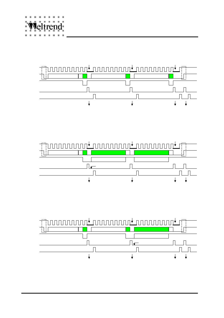
Composite Sync Signal Separator
Composite sync signal separator extract Vsync signal from HIN or SOGIN input pin by filtering pulses
which is less than 6us. The output Vsync signal will be widened about 5.5~6.5us. The output Hsync will
be replaced by 2us pulse during Vsync pulse.
The composite sync signal separator can handle H+V and H exclusive OR V signals. Fig.5 shows the
timing relationship of the extracted H and V sync signals.
If Hsync output do not want to insert pseudo H pulses (EXTRHS signal) during Vsync pulse, set BYPASS
bit can let HOUT pin output waveform same as Hsync input (Note: polarity can be controlled by HOPOL
bit).
Bypass H pulse
Bypass H pulse
Insert H pulse
5.5~6.5us
2us
2us
Hsync
Vsync
H+V
H XOR V
Bypass H pulse
Bypass H pulse
Insert H pulse
5.5~6.5us
2us
2us
Hsync
Vsync
H EORV
EXTRHS
EXTRVS
EXTRHS
EXTRVS
Fig. 6 Timing relationship of composite sync signal separator

WT62P1
Data Sheet Rev. 1.01
Weltrend Semiconductor, Inc.
Page 14
Free-running sync signal and self-test pattern
The self-generated free run sync signals are output from HOUT and VOUT pins when ENFREE bit is set.
Four kinds of standard VESA timings are selected by FREE1 and FREE0 bits.
Self-test pattern signal is output from PAT pin when ENPAT bit is set. PAT1 and PAT0 bits select
different self-test pattern.
Fig.7 Test Pattern
FREE2,1,0 bit value
X00
X01
010
011
110
111
F
H
Hor frequency
31.496KHz
48KHz
63.83KHz
81.25KHz
90.909KHz 106.195KHz
F
V
Ver frequency
59.993Hz
72.072Hz
59.878Hz
64.865Hz
84.8Hz
84.96Hz
T
HT
Hor total time
31.75us
20.833us
15.667us
12.333us
11us
9.417us
T
VT
Ver total time
16.669ms
13.875ms
16.7ms
15.417ms
11.792ms
11.771ms
T
HS
H sync time
3.833us
2.417us
1us
1.083us
1us
0.833us
T
HB
H Back porch +
H Left border
2 us
1.417us
2.417us
1.833us
1.583us
1.417us
T
HF
H Front porch +
H Right border
0.708us
1.125us
0.542us
0.375us
0.375us
0.292us
T
VS
V sync time
2 x T
HT
6 x T
HT
3 x T
HT
3 x T
HT
3 x T
HT
3 x T
HT
T
VB
V Back porch +
V Top border
33 X T
HT
23 x T
HT
38 x T
HT
46 x T
HT
44 x T
HT
46 x T
HT
T
VF
V Front porch +
V Bottom border
11 x T
HT
38 x T
HT
3 x T
HT
2 x T
HT
2 x T
HT
2 x T
HT
T
VIDEO
Video pulse width
41.67ns
41.67ns
41.67ns
41.67ns
41.67ns
41.67ns
PAT1 = 0 , PAT0 =
1
PAT1 = 1 , PAT0 = 1
PAT1 = 0 , PAT0 = 0
PAT1 = 1 , PAT0 = 0
HOUT
VOUT
T
HT
T
VT
T
HS
T
VS
HOUT
T
HT
T
HS
PAT
T
VEDIO
T
HF
T
HB
T
HB
Fig.8 Free-running sync signal and test pattern timing

WT62P1
Data Sheet Rev. 1.01
Weltrend Semiconductor, Inc.
Page 15
Clamp pulse
Clamp pulse is generated on either rising or falling edge of HOUT pin by setting the CLPEG bit. The
pulse width of clamp is specified by CLPPW bit. Output polarity is specified by CLPPO bit.
Sync Processor Control Registers
Name
Addr R/W Initial
Bit 7
Bit 6
Bit 5
Bit4
Bit 3
Bit 2
Bit 1
Bit 0
HV_CR1 0008h W
00h ENHOUT ENVOUT HOPOL
VOPOL
QUICK SEPART ENFREE ENPAT
HV_C
R
2 0009h W
00h
ENCLP
CLPEG
CLPPO
CLPPW
FREE1
FREE0
PAT1
PAT0
HV_C
R
3 000Ah W
x0h
--
--
--
--
--
SOG
FREE2
BYPASS
Bit Name
Description
ENHOUT
" 1" : Enable HOUT.
" 0" : Disable HOUT. Pin is configured as I/O port PD1.
ENVOUT
" 1" : Enable VOUT.
" 0" : Disable VOUT. Pin is configured as I/O port PD0.
HOPOL
" 1" : HOUT is positive polarity.
" 0" : HOUT is negative polarity.
VOPOL
" 1" : VOUT is positive polarity.
" 0" : VOUT is negative polarity.
QUICK
" 1" : Select 16ms time interval to count H pulses every 16.384ms.
" 0" : Select 32ms time interval to count H pulses every 32.768ms.
SEPART
" 1" : Enable sync separator circuit and use the extracted Vsync signal as VOUT.
" 0" : VOUT pin outputs Vsync from VIN pin
ENFREE
Enable free-running sync signal output on HOUT and VOUT pins when this bit is set.
ENPAT
" 1" : Enable self-test pattern output on PAT pin when this bit is set.
" 0" : Disable test pattern output. Pin is configured as I/O port PB3.
ENCLP
" 1" : Enable clamp pulse output on CLAMP pin.
" 0" : Disable clamp pulse output. Pin is configured as I/O port PA7.
CLPEG
" 1" : Clamp pulse follows HOUT signal's rising edge.
" 0" : Clamp pulse follows HOUT signal's falling edge.
0.542~0.625us/2.042~2.125us
HOUT
CLAMP
CLPPO=1
Fig. 9a Clamp pulse waveform (CLPEG=1)
CLAMP
CLPPO=0
HOUT
CLAMP
CLPPO=1
Fig. 9b Clamp pulse waveform (CLPEG=0)
CLAMP
CLPPO=0
0.542~0.625us/2.042~2.125us
0.542~0.625us/2.042~2.125us
0.542~0.625us/2.042~2.125us

WT62P1
Data Sheet Rev. 1.01
Weltrend Semiconductor, Inc.
Page 16
CLPPO
Select polarity of clamp pulse.
" 1" : Positive polarity
" 0" : Negative polarity
CLPPW
Select pulse width of clamp pulse.
" 1" : 2us
" 0" : 0.5us
FREE2,1,0
Select free-running sync signal frequency.
" 111" : 1600x1200@85Hz
H = 106.25kHz , V = 85Hz
" 110" : 1280x1024@85Hz
H = 91kHz , V = 85Hz
" 011" : 1600x1200@65Hz
H = 81kHz , V = 65Hz
" 010" : 1280x1024@60Hz
H = 64kHz , V = 60Hz
" x01" : 800x600@72Hz
H = 48kHz, V = 72Hz
" x00" : 640x480@60Hz
H = 31.4kHz, V = 60Hz
PAT1,0
Select test pattern.
" 00" : White picture
" 01" : 2x2 cross hatch
" 10" : Black picture
" 11" : Inverse 2x2 cross hatch
SOG
Select composite sync signal input source.
" 1" : Composite sync signal comes from SOGIN pin.
" 0" : Composite sync signal comes from HIN pin.
BYPASS
Select bypass the composite signal separator or not.
" 1" : HOUT pin outputs sync signal bypass the composite signal separator.
" 0" : HOUT pin outputs sync signal from the composite signal separator.

WT62P1
Data Sheet Rev. 1.01
Weltrend Semiconductor, Inc.
Page 17
Half Frequency Function
When ENHLFIO bit is set, Pin PB1 becomes half frequency input (HLFI) and Pin PB0 becomes half
frequency output (HLFO). The HALF bit controls the divided-by-two function is enabled or not.
Fig. 10 Half Hsync frequency
Half Frequency Output Control Register
Name
Addr R/W Initial
Bit 7
Bit 6
Bit 5
Bit4
Bit 3
Bit 2
Bit 1
Bit 0
HLF_CON 000Dh W
x0h
--
--
--
--
--
ENHFIO
HALF
HF_POL
Bit Name
Bit Description
ENHFIO
Enable half frequency input and output pins.
" 1" : PB1 and PB0 pins are half frequency input and output pins.
" 0" : PB1 and PB0 pins are I/O port.
HALF
" 1" : HLFO pin outputs half frequency from HLFI pin.
" 0" : HLFO pin outputs same frequency from HLFI pin.
HF_POL
" 1" : HLFO polarity is not same as HLFI.
" 0" : HLFO polarity is same as HLFI.
C
D
Q
QN
HLF_POL
HLFO
HALF
HLFI

WT62P1
Data Sheet Rev. 1.01
Weltrend Semiconductor, Inc.
Page 18
DDC Interface
The DDC interface is a slave mode I
2
C interface with DDC1 function. It is compatible with VESA
DDC1/2B standard. This interface not only can be used for DDC communication, but also can be applied
for factory alignment purpose.
When ENDDC bit is set, the outputs of SDA1 and SCL1 pins are open-drain type. The DDC function
depends on the DDC2 bit value. If DDC2 bit is " 0" , it is in DDC1 state. If DDC2 bit is " 1" , it is in DDC2
state
In DDC1 state, the data is shifted out to SDA1 pin on the rising edge of VSYNC clock. Data format is an
8-bit byte followed by a null bit (always " 1" ). Most significant bit (MSB) is transmitted first. Every time
when the ninth bit has been transmitted, the shift register will load a data byte from data buffer (DDC_TX
register). After loading data to the shift register, the data buffer becomes empty and generates an
interrupt. Program can check DDCRDY bit to load new data byte.
If a high to low transition occurs on SCL1 in DDC1 state, the SCLH2L bit will be set and generate an
interrupt. Program can set DDC2 bit to enter DDC2 state. If no valid DDC2 command is received within a
certain time (for example, 128 Vsync clocks or 2sec), program should clear DDC2 bit and back to DDC1
state to avoid noise interference.
The data format of DDC2 is
S
Address
R/W A
D7,D6,...., D0
A
D7,D6,...., D0
A
P
S : Start condition. A falling edge on SDA1 pin when SCL1 pin is high level.
P : Stop condition. A rising edge on SDA1 pin when SCL1 pin is high level.
A : Acknowledge bit.
0
means acknowledge and
1
means non-acknowledge.
Address : 7-bit device address.
R/W : Read/Write control bit, "1" is read and "0" is write.
D7,D6,...., D0 : data byte.
In DDC2 state, after START and valid address is received, it send out ACK(" 0" ) if the TXNAK1 bit is " 0" .
Otherwise the SDA1 pin outputs NACK(" 1" ). An interrupt will be generated after sending ACK bit and
SCL1 pin is pulled low to stop the clock for handshaking. In the interrupt routine, write DDC_AR0 register
will stop pulling low the SCL1 pin and clear the interrupt. The received address byte can be read in
DDC_RX register and also can use MATCH bit to identify what address is received. The Write or Read
operation can be checked by reading the DDCRW bit.
Write operation
After received the first byte (address byte), interrupt routine finds it is the first byte (FIRST=1) and write
operation (DDCRW=0), program should clear TX bit to " 0" (for receiving data) and write DDC_AR0
register (to release the SCL1 pin). Then the host sends out a data byte and SDA1 pin outputs ACK if
TXNACK bit is " 0" . An interrupt is generated after the ACK bit to inform CPU to read DDC_RX register.
When host finished transferring data, it will send STOP condition. When STOP condition is detected, the
STOP bit will be set and generates an interrupt. The interrupt routine can use the STOP bit to know the
data transfer is finished and start executing the received command.
Read operation
After received the first byte (address byte), interrupt routine finds it is the first byte (FIRST=1) and read
operation (DDCRW=1), program should set TX bit to " 1" , write data to DDC_TX register and write
DDC_AR0 register (to release the SCL1 pin). The host will output ACK after received a data byte. When
host wants to finish reading, it outputs NACK to stop communication. Program can read the RXACK1 bit
to check the acknowledge bit that host sends.

WT62P1
Data Sheet Rev. 1.01
Weltrend Semiconductor, Inc.
Page 19
DDC1 Timing
�
�
�
N
�
N
N
�
�
N
�
�
N
�
�
Pull low
SCL
START
�
Pull low
SCL
START
�
WT62P1
Data Sheet Rev. 1.01
Weltrend Semiconductor, Inc.
Page 20
DDC2 Timing
�
�
�
�
�
�
�
�
�
�
�
�
�
A
A
A
�
�
�
�
�
�
�
�
�
A
�
�
�
Pull low
SCL
Pull low
SCL
Pull low
SCL
Pull low
SCL
Pull low
SCL
Pull low
SCL
�
�
A
�
�
Pull low
SCL
Pull low
SCL
Pull low
SCL
A
START
START
START
STO
P
STO
P
STO
P

WT62P1
Data Sheet Rev. 1.01
Weltrend Semiconductor, Inc.
Page 21
DDC Receive Buffer Register
Name
Addr R/W Initial
Bit 7
Bit 6
Bit 5
Bit4
Bit 3
Bit 2
Bit 1
Bit 0
DDC_RX 0014h R
FFh
DRX7
DRX6
DRX5
DRX4
DRX3
DRX2
DRX1
DRX0
Bit Name
Description
DRX7 ... DRX0 DDC received data is stored in this register.
DDC Transmit Buffer Register
Name
Addr R/W Initial
Bit 7
Bit 6
Bit 5
Bit4
Bit 3
Bit 2
Bit 1
Bit 0
DDC_TX 0014h W
FFh
DTX7
DTX6
DTX5
DTX4
DTX3
DTX2
DTX1
DTX0
Bit Name
Description
DTX7 ... DTX0 This register stores the data to be transmitted
DDC Status Register
Name
Addr R/W Initial
Bit 7
Bit 6
Bit 5
Bit4
Bit 3
Bit 2
Bit 1
Bit 0
DDC_STA 0015h R
01h DDCRDY SCLH2L
DDC2
FIRST
STOP DDC2RW MATCH RXNAK1
Bit Name
Description
DDCRDY
When it is set, data buffer is ready to read/write or a SCL1 high to low transition in DDC1
state.
SCLH2L
Indicates a high to low transition on SCL1 pin in DDC1 state when it is set.
DDC2(R)
" 1" : Indicates it is in DDC2 state.
" 0" : Indicates it is in DDC1 state.
FIRST
Indicates the first byte (address) is received when this bit is set.
STOP
Indicates STOP condition is received when this bit is set.
DDC2RW
Indicates the received R/W bit after 7-bit address.
" 1" : Read
" 0" : Write
MATCH
" 1" : Address is equal to Address Register 1.
" 0" : The most significant 4 bits are equal to Address Register 0.
RXNAK1
Indicates the received acknowledge bit.
" 1" : NACK
" 0" : ACK
DDC Control Register
Name
Addr R/W Initial
Bit 7
Bit 6
Bit 5
Bit4
Bit 3
Bit 2
Bit 1
Bit 0
DDC_CON 0015h W
00h
ENDDC CLRH2L
DDC2
--
--
TX
--
TXNAK1
Bit Name
Description
ENDDC
" 1" : Enable DDC interface. PA0 and PA1 are configured as DDC interface.
" 0" : Disable DDC interface. PA0 and PA1 are configured as I/O port.
CLRH2L
Set this bit will reset SCLH2L bit.
DDC2(W)
" 1" : Set DDC2.
" 0" : Set DDC1.
TX
" 1" : Set transmit direction.
" 0" : Set receive direction.
TXNAK1
Determines the ACK bit to be transmitted.
" 1" : Transmit NACK.
" 0" : Transmit ACK.

WT62P1
Data Sheet Rev. 1.01
Weltrend Semiconductor, Inc.
Page 22
DDC Address Register 0
Name
Addr R/W Initial
Bit 7
Bit 6
Bit 5
Bit4
Bit 3
Bit 2
Bit 1
Bit 0
DDC_AR0 0016h W
x0h
DAR07
DAR06
DAR05
DAR04
--
--
--
ENAR0
Bit Name
Description
DAR07~
DAR04
4-bit DDC address to be compared. DAR07 is compared with the MSB of the received
address.
ENAR0
Enable DAR07- DAR04 to be compared when this bit is set.
DDC Address Register 1
Name
Addr R/W Initial
Bit 7
Bit 6
Bit 5
Bit4
Bit 3
Bit 2
Bit 1
Bit 0
DDC_AR1 0017h W
x0h
DAR17
DAR16
DAR15
DAR14
DAR13
DAR12
DAR11
ENAR1
Bit Name
Description
DAR17~
DAR11
7-bit DDC address to be compared. DAR17 is compared with the MSB of the received
address.
ENAR1
Enable DAR17- DAR11 to be compared when this bit is set.

WT62P1
Data Sheet Rev. 1.01
Weltrend Semiconductor, Inc.
Page 23
DDC Flow Chart
��
��
��
�
!"
!" #��
"
$%
"&'()*+"
*��
"
$%
,-.
��
/.
+"+.+
��
""
-/"
��
��
-/.
��
-012
��
""
/
3
��
��
-/.
��
/.
456+78
9-
!
��
��
*
!"
$%
��
��
-/.
��
"
��
��
��
�
!"

WT62P1
Data Sheet Rev. 1.01
Weltrend Semiconductor, Inc.
Page 24
Master/Slave I
2
C interface
The master/slave I
2
C interface is provided for communicating with other I
2
C devices in the monitor such
as EEPROM, OSD, deflection IC and so on.
Master Mode
To choose master mode, clear the SLAVE bit. The clock frequency can be programmed to 50KHz,
100kHz, 200kHz or 400KHz by setting MCLK1 and MCLK2 bits.
Send out START and the first byte (START, 7-bit address and R/W bit)
First, clear I2CRW bit to select transmitter mode and write first byte (7-bit address and R/W bit) to
MI2C_TX register. Then set MSTR bit, master will generate a START condition and send out the first
byte with the clock speed specified in MCLK1 and MCLK2 bits. After the whole data byte is transmitted
and the 9th bit is received, the MI2CRDY bit is set and generates an interrupt if it is enabled. The 9th bit
will be stored in RXNAK2 bit for checking the slave acknowledge or not. The SCL2 pin will keep low to
wait next byte operation.
Send out the following bytes
If it is a write command, write a data byte to MI2C_TX register, then write any value to I2C_AR register to
clear MI2CRDY bit. It will send out the data byte and store the acknowledge bit from slave in RXACK2 bit.
Again, the MI2CRDY bit is set after the acknowledge bit is received.
If it is a read command, set I2CRW bit to be receiver mode and write TXACK2 bit to determine what will
be sent on acknowledge bit, then write MI2C_AR register to clear I2CRDY bit and it will send out the
clock for receiving next byte. After the acknowledge bit is transmitted, the I2CRDY bit will be set. If
master wants to stop the read operation, send NACK on acknowledge bit to inform slave device.
Send out STOP
Set MSTOP bit will generate STOP condition.
Slave Mode
The slave mode operation is same as DDC interface in DDC2 state. First, set the SLAVE bit and set the
I2CRW bit to be receiver mode. When CPU is ready to receive, clear TXNAK2 bit. It will response ACK
when a START condition followed by an address (which is equal to I2C_ADR register) are received. An
interrupt can be generated if it is enabled and the R/W bit is stored in SRW bit for checking read/write
operation. After the ACK bit, SCL2 pin outputs low level to stop the clock for handshaking.
If a write command is received (SRW bit=0), read the I2C_RX register, clear I2CRW bit to receive next
byte, then write I2C_ADR to clear I2CRDY bit and stop pulling low the SCL2 pin for receiving next byte
from master. The output acknowledge bit is controlled by TX NAK2 bit.
If a read command is received (SRW bit=1), write data to I2C_TX register, clear I2CRW bit and write
I2C_ADR register to clear I2CRDY bit and stop pulling low the SCL2 pin for master sending out clock
The received acknowledge bit is stored in RXNAK2 bit.

WT62P1
Data Sheet Rev. 1.01
Weltrend Semiconductor, Inc.
Page 25
Master I
2
C Data Sequence
�
�
�
�
�
�
�
�
�
�
�
�
�
�
�
�
�
�
�
�
�
�
�
�
�
�
�
�
�
�
�
�
�
�
�
�
�
�
�
�

WT62P1
Data Sheet Rev. 1.01
Weltrend Semiconductor, Inc.
Page 26
Slave I
2
C Data Sequence
�
�
�
�
�
�
�
�
�
�
�
�
�
�
�
�
�
�
�
�
�
�
�
�
�
�
�
�
�
�
�
�
�
�
�

WT62P1
Data Sheet Rev. 1.01
Weltrend Semiconductor, Inc.
Page 27
I
2
C interface Status Register
Name
Addr R/W Initial
Bit 7
Bit 6
Bit 5
Bit4
Bit 3
Bit 2
Bit 1
Bit 0
I2C_STA 0010h
R
22h
--
--
BB
SFIRST
SSTOP
SRW
RXNAK2 I2CRDY
Bit Name
Description
BB
" 1" : Bus busy.
" 0" : Bus idle. Both SDA2 and SCL2 pins keep in high level for 5us after STOP condition.
SFIRST
This bit is set when received START and first byte in slave mode.
SSTOP
This bit is set when received STOP condition in slave mode.
SRW
Received R/W bit in slave mode.
" 1" : Read command is received.
" 0" : Write command is received.
RXNAK2
" 1" : NACK is received.
" 0" : ACK is received.
I2CRDY
This bit is set when a byte is received, transmitted or STOP condition is detected.
I
2
C interface Control Register
Name
Addr R/W Initial
Bit 7
Bit 6
Bit 5
Bit4
Bit 3
Bit 2
Bit 1
Bit 0
I2C_CON 0010h W
02h
ENI2C
MCLK1
MCLK0
MSTR
MSTOP
I2CRW
TXNAK2
SLAVE
Bit Name
Description
ENI2C
" 1" : Enable I2C interface.
" 0" : Pin PB5 and pin PB4 are I/O port.
MCLK1,0
Select SCL clock in master mode
" 00" : 400KHz
" 01" : 100KHz
" 11" : 200KHz
" 10" : 50KHz
MSTR
Output START condition in master mode when this bit is set.
MSTOP
Output STOP condition in master mode when this bit is set.
I2CRW
" 0" : Transmitter , " 1" : Receiver in master mode.
" 1" : Transmitter , " 0" : Receiver in slave mode
(" 0" : I2C write mode, " 1" : I2C read mode. )
TXNAK2
" 1" : Output NACK.
" 0" : Output ACK. It will pull low the SDA2 pin on acknowledge bit.
SLAVE
" 1" : Slave mode.
" 0" : Master mode.
I
2
C interface Transmit/Receive Buffer Register
Name
Addr R/W Initial
Bit 7
Bit 6
Bit 5
Bit4
Bit 3
Bit 2
Bit 1
Bit 0
I2C_TX 0011h
W
xxh
MTX7
MTX6
MTX5
MTX4
MTX3
MTX2
MTX1
MTX0
I2C_RX 0011h
R
xxh
MRX7
MRX6
MRX5
MRX4
MRX3
MRX2
MRX1
MRX0
I
2
C interface Address Register
Name
Addr R/W Initial
Bit 7
Bit 6
Bit 5
Bit4
Bit 3
Bit 2
Bit 1
Bit 0
I2C_ADR 0012h
W
xxh
SAR7
SAR6
SAR5
SAR4
SAR3
SAR2
SAR1
--
Bit Name
Description
SAR7 ~ SAR1 7-bit address to be compared in slave mode.
WT62P1
Data Sheet Rev. 1.01
Weltrend Semiconductor, Inc.
Page 28
Master I
2
C Flow Chart
�
�
�
!"
�
#$
��
%&#'#&&$
(
)*+�
,*�
-
#$*+.�
+.
,*/0�
1
2++2(
).�
%&&##(
)*+�
2++2(
).�
+.
#34%&&
%&&##(
)*+�
2++2(
).�
,*/0�
1
2++2(
).�
��
$#"
*+.�
2++2(
).�
$#&
)+
,*/0�
1
2++2(
).�
2++2(
).�
$#&
)+
�

WT62P1
Data Sheet Rev. 1.01
Weltrend Semiconductor, Inc.
Page 29
Master I
2
C (restart mode) Flow Chart
�
�
�
!"
�
#$
��
%&#'#&&$
(
)*+�
,*�
-
#$*+.�
+.
%&&##(
)*+�
/++/(
).�
��
$#
*+.�
/++/(
).�
$#&
)+
,*23�
4
/++/(
).�
/++/(
).�
$#&
)+
+.
%&#'#&&$
(
)*+�
,*�
-
/++/(
).�
+.
,*23�
4
/++/(
).�

WT62P1
Data Sheet Rev. 1.01
Weltrend Semiconductor, Inc.
Page 30
Slave I
2
C Flow Chart
�
�
�
�
!
�
"
�
#$%
"&
!
�
"
�
"
�
'(
)*
�
�
�

WT62P1
Data Sheet Rev. 1.01
Weltrend Semiconductor, Inc.
Page 31
Timer
It is a 6-bit down counter with 2-bit prescaler. The time base is selected by PS1 and PS0 bits. Timer
starts counting when writing data to TIMER register. When the counter reaches zero, the counter stops
and sets interrupt flag (IF_TMR). If program wants to start the timer again, write data to TIMER register.
Fig.11 Block diagram of Timer
Timer Register
Name
Addr R/W Initial
Bit 7
Bit 6
Bit 5
Bit4
Bit 3
Bit 2
Bit 1
Bit 0
TIMER 0018h
W
00h
PS1
PS0
TIM5
TIM4
TIM3
TIM2
TIM1
TIM0
Bit Name
Bit Description
PS1,PS0
Prescaler of timer.
" 00" : time base = 0.256ms
" 01" : time base = 0.512ms
" 10" : time base = 1.024ms
" 11" : time base = 4.096ms
TIM5 ~ TIM0 Timer period = time base x (6-bit data)
0.512ms
1.024ms
4.096ms
0.256ms
Time base
Selector
PS1 PS0
6-Bit Timer
TIM0 TIM1 TIM2 TIM3 TIM4 TIM5
IF_TMR
IE_TMR

WT62P1
Data Sheet Rev. 1.01
Weltrend Semiconductor, Inc.
Page 32
A/D converter
The Analog-to-Digital Converter (ADC) has 6-bit resolution with four selectable input channels. When an
input channel is selected, it will reset the ADC_DA register and start converting. After the conversion is
done, the ADRDY bit is set and valid data is stored in AD5~AD0 bits. The total conversion time is from
4.096ms to 8.192ms. If program want to make a new conversion, write ADC_CH register again and it will
start another conversion.
ADC Data Register
Name
Addr R/W Initial
Bit 7
Bit 6
Bit 5
Bit4
Bit 3
Bit 2
Bit 1
Bit 0
ADC_DA 001Ah
R
0xh
ADRDY
--
AD5
AD4
AD3
AD2
AD1
AD0
Bit Name
Bit Description
ADRDY
ADC data is ready to read when this bit is set.
AD5 ~ AD0
ADC data.
ADC Channel Select Register
Name
Addr R/W Initial
Bit 7
Bit 6
Bit 5
Bit4
Bit 3
Bit 2
Bit 1
Bit 0
ADC_CH 001Ah W
00h
--
--
--
--
CH3
CH2
CH1
CH0
Bit Name
Bit Description
CH3
Select AD3 pin connect to ADC when this bit is set.
CH2
Select AD2 pin connect to ADC when this bit is set.
CH1
Select AD1 pin connect to ADC when this bit is set.
CH0
Select AD0 pin connect to ADC when this bit is set.
Fig.12 Block diagram of ADC
CH3
AD2
AD1
AD0
AD3
CH2
CH1
CH0
Comparator
Resistor Array
6-bit Counter
ADRDY

WT62P1
Data Sheet Rev. 1.01
Weltrend Semiconductor, Inc.
Page 33
A/D Converter Flow Chart
�
�
�
�
�

WT62P1
Data Sheet Rev. 1.01
Weltrend Semiconductor, Inc.
Page 34
Interrupt Control
There are two interrupt vectors of CPU. The high priority interrupt INT0 (vector in $FFFAh and $FFFBh)
is used for DDC interface interrupt. The low priority INT1 (vector in $FFFEh and $FFFFh) is ORed by six
interrupt sources. Each interrupt can be enabled/disabled independently by programming INT_EN
register and identified by INT_FLAG register.
DDC interface interrupt
Interrupt Condition
Clear Interrupt
Transmit data buffer is empty in DDC1 mode.
Write data to DDC_RX register.
A high to low transition on SCL1 pin in DDC1
mode.
Set CLRH2L bit in DDC_CON register and clear it .
Receive one byte in DDC2 mode.
Write address to DDC_AR0 register.
Transmit data buffer is empty in DDC2 mode.
Write address to DDC_AR0 register.
Received a STOP condition in DDC2 mode.
Write address to DDC_AR0 register.
I
2
C interface interrupt
Interrupt Condition
Clear Interrupt
After transmit a byte.
Write address to MI2C_AR register.
After receive a byte.
Write address to MI2C_AR register.
Received a STOP condition.
Write address to MI2C_AR register.
USB interrupt
Interrupt Condition
Clear Interrupt
Endpoint 0 IN token fail.
Set CLR_INT in USB_FPC register and clear.
Endpoint 0 IN token success.
Set CLR_INT in USB_FPC register and clear.
Reset transaction happened.
Set CLR_INT in USB_FPC register and clear.
Endpoint 1 IN token fail.
Set CLR_INT in USB_FPC register and clear.
Endpoint 1 IN token success.
Set CLR_INT in USB_FPC register and clear.
OUT token is finished.
Set CLR_INT in USB_FPC register and clear.
SETUP token is received.
Set CLR_INT in USB_FPC register and clear.
Sync Processor interrupt
Interrupt Condition
Clear Interrupt
Latch a new H frequency to HFREQ_H and
HFREQ_L register every 32.768ms or 16.384ms.
Read HFREQ_H Register.
Timer interrupt
Interrupt Condition
Clear Interrupt
Timer expired.
Write a value to TIMER register
IRQ pin interrupt
Interrupt Condition
Clear Interrupt
Low level or falling edge on /IRQ pin.
Set CLRIRQ bit in IRQ_CON register and clear it .
Vsync interrupt
Interrupt Condition
Clear Interrupt
Leading edge of VOUT pin signal.
Set CLRVSO bit in IRQ_CON register and clear it .

WT62P1
Data Sheet Rev. 1.01
Weltrend Semiconductor, Inc.
Page 35
Interrupt Flag Register
Name
Addr R/W Initial
Bit 7
Bit 6
Bit 5
Bit4
Bit 3
Bit 2
Bit 1
Bit 0
INT_FLAG 001Bh R
00h
IF_DDC IF_MI2C IF_USB IF_SYNC IF_TMR
IF_IRQ
IF_VSO
--
Bit Name
Bit Description
IF_DDC
Indicate DDC interrupt when this bit is set.
IF_MI2C
Indicate I2C interrupt when this bit is set.
IF_USB
Indicate USB interrupt when this bit is set.
IF_SYNC
Indicate sync processor interrupt when this bit is set.
IF_TMR
Indicate Timer interrupt when this bit is set.
IF_IRQ
Indicate IRQ interrupt when this bit is set.
IF_VSO
Indicate VOUT interrupt when this bit is set.
Interrupt Enable Register
Name
Addr R/W Initial
Bit 7
Bit 6
Bit 5
Bit4
Bit 3
Bit 2
Bit 1
Bit 0
INT_EN
001Bh W
00h
IE_DDC IE_MI2C IE_USB IE_SYNC IE_TMR
IE_IRQ
IE_VSO
--
Bit Name
Bit Description
IE_DDC
Enable DDC interrupt when this bit is set.
IE_MI2C
Enable I2C interrupt when this bit is set.
IE_USB
Enable USB interrupt when this bit is set.
IE_SYNC
Enable sync processor interrupt when this bit is set.
IE_TMR
Enable Timer interrupt when this bit is set.
IE_IRQ
Enable IRQ interrupt when this bit is set.
IE_VSO
Enable VOUT interrupt when this bit is set.
Interrupt Source Register
Name
Addr R/W Initial
Bit 7
Bit 6
Bit 5
Bit4
Bit 3
Bit 2
Bit 1
Bit 0
INT_SRC 001Ch R
--
--
--
SYNC
TIMER
IRQ
VSO
--
Bit Name
Bit Description
SYNC
Indicate H frequency counter is ready to read when this bit is set..
TIMER
Indicate Timer expired when this bit is set.
IRQ
Indicate a low level or falling edge occurs on IRQ pin when this bit is set.
VSO
Indicate a leading edge occurs on VOUT pin when this bit is set.
IRQ Control Register
Name
Addr R/W Initial
Bit 7
Bit 6
Bit 5
Bit4
Bit 3
Bit 2
Bit 1
Bit 0
IRQ_CON 001Ch W
00h
--
--
--
--
--
CLRIRQ CLRVSO IRQ_EG
Bit Name
Bit Description
CLRVSO
Clear VOUT interrupt when this bit is set.
CLRIRQ
Clear IRQ interrupt when this bit is set.
IRQ_EG
Select IRQ pin interrupt type.
" 1" : Falling edge
" 0" : Low level
Watchdog Timer
Watchdog timer will generate a reset pulse if CPU does not write WDT register within 259.072ms or
518.144ms. This function can be disable by setting DISWDT bit.

WT62P1
Data Sheet Rev. 1.01
Weltrend Semiconductor, Inc.
Page 36
Watchdog Timer Register
Name
Addr R/W Initial
Bit 7
Bit 6
Bit 5
Bit4
Bit 3
Bit 2
Bit 1
Bit 0
WDT
001Dh
W
00h
--
--
--
--
--
--
DISWDT
WDT
Bit Name
Description
DISWDT
" 1" : Disable Watchdog Timer.
" 0" : Enable Watchdog Timer.
WDT
" 1" : Watchdog Timer reset period is 518.144ms +8.096ms.
" 0" : Watchdog Timer reset period is 259.072ms +8.096ms.
Function Configuration Register
This register controls the special configuration of WT62P1.
Name
Addr R/W Initial
Bit 7
Bit 6
Bit 5
Bit4
Bit 3
Bit 2
Bit 1
Bit 0
OPTION 0FFFh W
00h
ENV33
--
--
--
DISRST
STEST
BANK3
BANK2
Bit Name
Bit Value = "1"
Bit Value = "0"
BANK2
Enable RAM 0200h~027Fh
Disable RAM 0200h~027Fh
BANK3
Enable RAM 0280h~02FFh
Disable RAM 0280h~02FFh
STEST
For IC test only. Do not set this bit.
For normal operation.
DISRST
Disable illegal address reset.
Enable illegal address reset.
ENV33
Enable 3.3V regulator.
Disable 3.3V regulator.

WT62P1
Data Sheet Rev. 1.01
Weltrend Semiconductor, Inc.
Page 37
PWM
There are 14 PWMs provided.
PWM0 ~ PWM1 : +5V open-drain output.
PWM2 ~ PWM3 : +10V open-drain output.
PWM4 ~ PWM7 : +5V open-drain output, shared with I/O port D.
PWM8 ~ PWM13 : +5V push-pull output, shared with I/O port A.
The corresponding PWM register controls the PWM duty cycle. Duty cycle range is from 0/256 to
255/256.
LSB 3-bit of PWM register determines which frame will be extended two Tosc. ( Tosc = 1/12MHz)
000 : no extended pulse.
001 : extend two Tosc in frame 4.
010 : extended two Tosc in frame 2 and 6.
011 : extended two Tosc in frame 2, 4 and 6.
100 : extended two Tosc in frame 1, 3, 5 and 7.
101 : extended two Tosc in frame 1, 3, 4, 5 and 7.
110 : extended two Tosc in frame 1, 2, 3, 5, 6 and 7.
111 : extended two Tosc in frame 1, 2, 3, 4, 5, 6 and 7.
MSB 5-bit of PWM register determines 0/32 to 31/32 duty cycle in each frame.
Fig. 13 PWM output waveform
PWM=00001000
Frame 0 Frame 1 Frame 2 Frame 3 Frame 4
Frame 5 Frame 6 Frame 7
PWM=00001001
2 Tosc
2 Tosc
4 Tosc
32 Tosc
PWM=00010010
4 Tosc
6 Tosc
4 Tosc
6 Tosc
4 Tosc
4 Tosc
4 Tosc
4 Tosc
256
Tosc
2 Tosc
2 Tosc
2 Tosc
2 Tosc
2 Tosc
2 Tosc

WT62P1
Data Sheet Rev. 1.01
Weltrend Semiconductor, Inc.
Page 38
PWM Registers
Name
Addr R/W Initial
Bit 7
Bit 6
Bit 5
Bit4
Bit 3
Bit 2
Bit 1
Bit 0
PWM0
0020h R/W 80h
PWM0
7
PWM0
6
PWM0
5
PWM0
4
PWM0
3
PWM0
2
PWM0
1
PWM0
0
PWM1
0021h R/W 80h
PWM1
7
PWM1
6
PWM1
5
PWM1
4
PWM1
3
PWM1
2
PWM1
1
PWM1
0
PWM2
0022h R/W 80h
PWM2
7
PWM2
6
PWM2
5
PWM2
4
PWM2
3
PWM2
2
PWM2
1
PWM2
0
PWM3
0023h R/W 80h
PWM3
7
PWM3
6
PWM3
5
PWM3
4
PWM3
3
PWM3
2
PWM3
1
PWM3
0
PWM4
0024h R/W 80h
PWM4
7
PWM4
6
PWM4
5
PWM4
4
PWM4
3
PWM4
2
PWM4
1
PWM4
0
PWM5
0025h R/W 80h
PWM5
7
PWM5
6
PWM5
5
PWM5
4
PWM5
3
PWM5
2
PWM5
1
PWM5
0
PWM6
0026h R/W 80h
PWM6
7
PWM6
6
PWM6
5
PWM6
4
PWM6
3
PWM6
2
PWM6
1
PWM6
0
PWM7
0027h R/W 80h
PWM7
7
PWM7
6
PWM7
5
PWM7
4
PWM7
3
PWM7
2
PWM7
1
PWM7
0
PWM8
0028h R/W 80h
PWM8
7
PWM8
6
PWM8
5
PWM8
4
PWM8
3
PWM8
2
PWM8
1
PWM8
0
PWM9
0029h R/W 80h
PWM9
7
PWM9
6
PWM9
5
PWM9
4
PWM9
3
PWM9
2
PWM9
1
PWM9
0
PWM10
002Ah R/W 80h PWM10
7
PWM10
6
PWM10
5
PWM10
4
PWM10
3
PWM10
2
PWM10
1
PWM10
0
PWM11
002Bh R/W 80h PWM11
7
PWM11
6
PWM11
5
PWM11
4
PWM11
3
PWM11
2
PWM11
1
PWM11
0
PWM12
002Ch R/W 80h PWM12
7
PWM12
6
PWM12
5
PWM12
4
PWM12
3
PWM12
2
PWM12
1
PWM12
0
PWM13
002Dh R/W 80h PWM13
7
PWM13
6
PWM13
5
PWM13
4
PWM13
3
PWM13
2
PWM13
1
PWM13
0
PWM_EN1 002Eh W
00h
--
--
--
--
EPWM7 EPWM6 EPWM5 EPWM4
PWM_EN2 002Fh W
00h
--
--
EPWM13 EPWM12 EPWM11 EPWM10 EPWM9 EPWM8
Bit Name
Description
PWMX
7
~ PWMX
0
Select duty cycle of PWM output.
00000000 : duty cycle = 0
00000001 : duty cycle = 1/256
00000010 : duty cycle = 2/256
:
11111110 : duty cycle = 254/256
11111111 : duty cycle = 255/256
EPWMx
Enable corresponding PWM output. ( x from 4 to 13) when it is set.

WT62P1
Data Sheet Rev. 1.01
Weltrend Semiconductor, Inc.
Page 39
USB Interface
The USB interface contains tranceiver, Serial Interface Engine (SIE), 3.3V voltage regulator, FIFOs for
endpoint 0/1 and interface logic circuit.
Fig.14 Block diagram of USB function
3.3V Regulator
The 3.3V regulator generates power for USB tranceiver. It can be enable/disable by the bit-7 of OPTION
register ($0FFFH).
Tranceiver
It is capable of transmitting/receiving serial data at 1.5Mbit/s and complies with USB specification 1.0.
Serial Interface Engine (SIE)
The SIE supports :
Packet protocol sequencing
SOP,EOP,RESUME,RESET signal detection/generation
Clock/data separation
NRZI data encoding/decoding and bit-stuffing
CRC generation and checking (Token and Data)
Packet ID (PID) decoding/generation
Serial-to-Parallel/Parallel-to-Serial conversion
Interface Logic
Main functions of the interface logic circuit are :
USB address and endpoint decoding
USB endpoint level flow control
Maintain state of data toggle bits
Interface to CPU
Serial
Interface
Engine
Tranceiver
D+
D-
+3.3V
EP0 OUT FIFO
EP0 IN FIFO
EP1 IN FIFO
Data Bus
Interface Logic
Interrupt
1.5K
3.3V Regulator
VDD

WT62P1
Data Sheet Rev. 1.01
Weltrend Semiconductor, Inc.
Page 40
FIFO
The FIFO is used to buffer USB data. There are three FIFOs : Endpoint 0 has IN FIFO (transmit) and
OUT FIFO (receive), Endpoint 1 has IN FIFO only. Each FIFO has 8 bytes depth. The architecture of
FIFO is show as blow.
DATA OUT
DATA IN
Read Pointer
Write Pointer
8
7
6
5
4
3
2
1
0

WT62P1
Data Sheet Rev. 1.01
Weltrend Semiconductor, Inc.
Page 41
USB Address Register
Name
Addr R/W Initial
Bit 7
Bit 6
Bit 5
Bit4
Bit 3
Bit 2
Bit 1
Bit 0
USB_ADR 0030h W
00h EN_USB
UAD6
UAD5
UAD4
UAD3
UAD2
UAD1
UAD0
Bit Name
Description
EN_USB
" 1" : Enable USB function and connect D- pull up resistor.
" 0" : Disable USB function and disconnect D- pull up resistor.
UAD6 ~ UAD0 USB device address.
USB Interrupt Control Register
Name
Addr R/W Initial
Bit 7
Bit 6
Bit 5
Bit4
Bit 3
Bit 2
Bit 1
Bit 0
USB_ICR 0031h W
00h
--
ENSTAL1 ENOK1
ENRST ENSTAL0 ENOK0
ENOUT
ENSUP
Bit Name
Description
ENSTAL1
Enable Endpoit1 IN token stall interrupt.
ENOK1
Enable Endpoit1 IN token success interrupt.
ENRST
Enable RESET transaction interrupt.
ENSTAL0
Enable Endpoit0 IN token stall interrupt .
ENOK0
Enable Endpoit0 IN token success interrupt.
ENOUT
Enable OUT token success interrupt.
ENSUP
Enable ETUP token finished interrupt.
USB Interrupt Status Register
Name
Addr R/W Initial
Bit 7
Bit 6
Bit 5
Bit4
Bit 3
Bit 2
Bit 1
Bit 0
USB_ISR 0031h R
00h
ACTIVE
STALL1
EP1OK
RESET
STALL0
EP0OK
OUT
SETUP
Bit Name
Description
ACTIVE
" 1" : Indicate the USB bus is active
" 0" : Indicate the USB bus is suspended.
EP1STAL
When this bit is set, it indicates Endpoit1 IN token stall or failed.
EP1OK
When this bit is set, it indicates Endpoit1 IN token success (ACK).
RESET
When this bit is set, it indicates RESET transaction happened
EP0STAL
When this bit is set, it indicates Endpoit0 IN token stall or failed.
EP0OK
This bit is set when Endpoit0 IN token finished and ACK token has received.
OUT
When this bit is set, it indicates OUT token is received
SETUP
When this bit is set, it indicates SETUP token is received
USB Endpoint 0 FIFO
Name
Addr R/W Initial
Bit 7
Bit 6
Bit 5
Bit4
Bit 3
Bit 2
Bit 1
Bit 0
USB_FIFO0 0032h R/W
xxh
F0D7
F0D6
F0D5
F0D4
F0D3
F0D2
F0D1
F0D0
Bit Name
Description
F0D7 ~ F0D0
Endpoint 0 FIFO.

WT62P1
Data Sheet Rev. 1.01
Weltrend Semiconductor, Inc.
Page 42
USB FIFO Pointer Status Register
Name
Addr R/W Initial
Bit 7
Bit 6
Bit 5
Bit4
Bit 3
Bit 2
Bit 1
Bit 0
USB_FPS 0033h R
--
TOGOUT UNDRN TXOVF
RXEMP
UCNT3
UCNT2
UCNT1
UCNT0
Bit Name
Description
TOGOUT
" 1" : Indicates the Data packet type of receive data is Data1.
" 0" : Indicates the Data packet type of receive data is Data0.
UNDRN
FIFO Under-run. When this bit is set, it indicates reading EP0 OUT FIFO when it is
empty..
TXOVF
Transmit FIFO overflow. When this bit is set, it indicates writing data to EP0 IN FIFO
when it is full.
RXEMP
Receive FIFO empty. When this bit is set, it indicates EP0 OUT FIFO is empty.
UCNT3~UCNT0 Read pointer of EP0 OUT FIFO. The value indicates how many data byte stored in
EP0 IN FIFO.
" 0000" : 0 byte
" 0001" : 1 byte
:
" 1000" : 8 byte
USB FIFO Pointer Control Register
Name
Addr R/W Initial
Bit 7
Bit 6
Bit 5
Bit4
Bit 3
Bit 2
Bit 1
Bit 0
USB_FPC 0033h W
00h
--
--
CLRACT CLRINT REP0RP REP0WP REP1RP REP1WP
Bit Name
Description
CLRACT
When this bit is set, it clears the ACTIVE bit. (Bit7 of USB_ISR register)
CLRINT
When this bit is set, it clears the interrupt source
REP0RP
When this bit is set, it resets the read pointer of EP0 IN FIFO.
REP0WP
When this bit is set, it resets the write pointer of EP0 IN FIFO.
REP1RP
When this bit is set, it resets the read pointer of EP1 IN FIFO.
REP1WP
When this bit is set, it resets the write pointer of EP1 IN FIFO.
USB Endpoint 0 Control Register
Name
Addr R/W Initial
Bit 7
Bit 6
Bit 5
Bit4
Bit 3
Bit 2
Bit 1
Bit 0
USB_CR0 0034h W
00h RESUME
--
--
OUT0STL ENOUT0 IN0STL
EP0VAL EP0TOG
Bit Name
Description
RESUME
Send Resume signal to Host.
OUT0STL
Set EP0-OUT pipe stall when this bit is " 1" .
ENOUT0
Enable EP0-OUT pipe when this bit is " 1" .
IN0STL
Set EP0-IN pipe stall when this bit is " 1" .
EP0VAL
Set EP0-IN FIFO ready to send data when this bit is " 1" .
EP0TOG
Set data packet type of EP0-IN pipe will send
USB Endpoint 1 FIFO
Name
Addr R/W Initial
Bit 7
Bit 6
Bit 5
Bit4
Bit 3
Bit 2
Bit 1
Bit 0
USB_FIFO1 0035h W
xxh
F1D7
F1D6
F1D5
F1D4
F1D3
F1D2
F1D1
F1D0
Bit Name
Description
F1D7 ~ F1D0
Endpoint 1 IN FIFO.

WT62P1
Data Sheet Rev. 1.01
Weltrend Semiconductor, Inc.
Page 43
USB Endpoint1 Control Register
Name
Addr R/W Initial
Bit 7
Bit 6
Bit 5
Bit4
Bit 3
Bit 2
Bit 1
Bit 0
USB_CR1 0036h W
x8h
--
--
--
--
ENEP1
EP1STL EP1VAL EP1TOG
Bit Name
Descriptions
ENEP1
Enable EP1-IN pipe when this bit is " 1" .
EP1STL
Set EP1-IN pipe stall when this bit is " 1" .
EP1VAL
Set EP1-IN FIFO ready to send data when this bit is " 1" .
EP1TOG
Set data packet type of EP1-IN pipe. When this bit is " 1, it is DATA1.

WT62P1
Data Sheet Rev. 1.01
Weltrend Semiconductor, Inc.
Page 44
ELECTRICAL CHARACTERISTICS
Absolute Maximum Ratings
Parameter
Min.
Max.
Units
DC Supply Voltage (VDD)
-0.3
7.0
V
Input and output voltage with respect to Ground
-0.3
VDD+0.3
V
Storage temperature
-25
125
o
C
Ambient temperature with power applied
-10
85
o
C
*Note: Stresses above those listed may cause permanent damage to the devices
D.C Characteristics (VDD=5.0V
±
±
±
±
5%, Ta=0-70
∞
C)
Symbol
Parameter
Condition
Min.
Typ.
Max.
Units
V
DD
Supply Voltage
4.5
5
5.5
V
V
33
3.3V regulator output voltage
3.0
3.3
3.6
V
V
IH
Input High Voltage
0.7V
DD
--
V
DD
+0.3
V
V
IL
Input Low Voltage
-0.3
--
0.2V
DD
V
V
IH,SYNC
Sync Input High Voltage
2.2
--
V
DD
+0.3
V
V
IL,SYNC
Sync Input Low Voltage
-0.3
--
0.8
V
V
IH,RES
Reset Input High Voltage
2.2
--
V
DD
+0.3
V
V
IL,RES
Reset Input Low Voltage
-0.3
--
0.8
V
V
OH
Output High Voltage
I
OH
= -6mA
4
4.5
V
DD
V
V
OL
Output Low Voltage
I
OL
= 6mA
0
0.26
0.4
V
R
DH,USB
Output impedance (High
state)
8
ohm
R
OL,USB
Output impedance (Low
state)
8
ohm
I
IL,SYNC
Input Leakage Current
HSYNC and VSYNC pins
0V <V
IN
< V
DD
-1
--
1
µ
A
R
PH
Pull High Resistance
20
50
Kohm
I
DD
Operating Current
F
OSC
= 12MHz, No load
12
30
mA
V
RESET
Low V
DD
Reset Voltage
3.6
3.9
4.2
V

WT62P1
Data Sheet Rev. 1.01
Weltrend Semiconductor, Inc.
Page 45
A.C Characteristics (VDD=5.0V
±
±
±
±
5%, fosc=12MHz, Ta=0-70
∞
C)
/RESET and /IRQ Timing
Symbol
Parameter
Min.
Typ.
Max.
Units
t
LOW,RES
/RESET pin low pulse
167
-
-
ns
t
LOW,IRQ
/IRQ low pulse (level trigger)
167
-
-
ns
SYNC Processor Timing
Symbol
Parameter
Min.
Typ.
Max.
Units
t
HIGH,SYNC
HSYNC and VSYNC high time
167
-
-
ns
t
LOW,SYNC
HSYNC and VSYNC low time
167
-
-
ns
DDC1 Timing
Symbol
Parameter
Min.
Typ.
Max.
Units
t
VAA,DDC1
SDA1 output valid from VSYNC rising edge
125
-
500
ns
VSYNC
�
SDA1
Bit 0 (LSB)
Bit 7 (MSB)
Null Bit
t
HIGH,SYNC
t
LOW,SYNC
HSYNC
VSYNC
RESET
IRQ

WT62P1
Data Sheet Rev. 1.01
Weltrend Semiconductor, Inc.
Page 46
DDC2B Timing
Symbol
Parameter
Min.
Typ.
Max.
Units
f
SCL
SCL1 input clock frequency
0
-
100
kHz
t
BF
Bus free time
2
-
-
us
t
HD,START
Hold time for START condition
1
-
-
us
t
SU,START
Set-up time for START condition
1
-
-
us
t
HIGH,SCL
SCL1 clock high time
1
-
-
us
t
LOW,SCL
SCL1 clock low time
1
-
-
us
Hold time for DATA input
0
-
-
ns
t
HD,DATA
Hold time for DATA output
167
-
-
ns
Set-up time for DATA input
167
-
-
ns
t
SU,DATA
Set-up time for DATA output
334
-
-
ns
t
RISE,DDC
SCL1 and SDA1 rise time
-
-
1
us
t
FALL.DDC
SCL1 and SDA1 fall time
-
-
300
ns
t
SU,STOP
Set-up time for STOP condition
2
-
-
us
SDA1
SCL1

WT62P1
Data Sheet Rev. 1.01
Weltrend Semiconductor, Inc.
Page 47
USB Timing
Symbol
Parameter
Min.
Typ.
Max.
Units
t
RISE,USB
D+ and D- Rise Time
75
300
ns
t
FALL,USB
D+ and D- Fall Time
75
300
ns
t
RFM
D+ and D- Rise/Fall Time Matching
70
130
%
V
CROSS
Crossover point
1.3
2.0
V
D+ , D-
t
RISE,USB
t
RISE,USB

WT62P1
Data Sheet Rev. 1.01
Weltrend Semiconductor, Inc.
Page 48
TYPICAL APPLICATION CIRCUIT
Crystal Oscillator
Reset Pin and 3.3V Regulator
PWM Output

WT62P1
Data Sheet Rev. 1.01
Weltrend Semiconductor, Inc.
Page 49
Hsync, Vsync and DDC Interface Protection