
Weltrend Semiconductor, Inc.
2F, No. 24, Industry E. 9
th
RD., Science-Based Industrial Park, Hsin-Chu, Taiwan
TEL:886-3-5780241 FAX:886-3-5794278.5770419
Email:support@weltrend.com.tw
WT6801
Monitor On-Screen Display
Data Sheet
REV. 1.0
June 27, 2000
The information in this document is subject to change without notice.
©
Weltrend Semiconductor, Inc. All Rights Reserved.
WT6801
Data Sheet Rev. 1.0
Weltrend Semiconductor, Inc.
Page 2
GENERAL DESCRIPTION
The WT6801 is designed to display color symbols or characters onto monitor. By storing display data in its
RAM and control information in the registers via I
2
C interface, WT6801 can carry out screen refresh without
any MCU supervision.
FEATURES
∑
Programmable horizontal resolutions up to 1530 dots per line
∑
Horizontal frequency up to 120KHz
∑
On-chip PLL up to 96MHz
∑
Fully programmable character array of 15 rows by 30 columns
∑
12x18 dot matrix per character
∑
256 characters and graphic symbols ROM including 16 multi-color fonts
∑
8 colors per display character
∑
7 colors per display character background
∑
4 programmable windows
∑
Double character height and width control
∑
Programmable character height (18 to 71 lines)
∑
Programmable row-to-row spacing
∑
Programmable vertical and horizontal positioning for display screen center
∑
Bordering, shadowing and blinking effect
∑
Fade-in/Fade-out effect
∑
Video timing capture for auto sizing
∑
I
2
C interface with slave address $7AH
∑
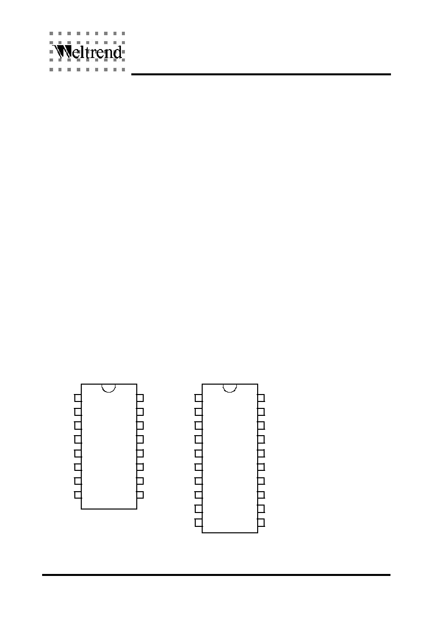
Package type : 16-pin and 20-pin plastic DIP/SOP
PIN CONFIGURATION
11
12
16
15
14
13
17
18
19
20
10
9
8
7
6
5
4
3
2
1
BIN
BOUT
CLKIN
FBKG
GIN
GOUT
HFLB
HFX
LF
RIN
ROUT
SCL
SDA
VCO
VDD
VDDA
VFLB
VSS
VSSA
9
10
11
12
16
15
14
13
8
7
6
5
4
3
2
1
BOUT
CLKIN
FBKG
GOUT
HFLB
LF
ROUT
SCL
SDA
VCO
VDD
VDDA
VFLB
VSS
VSSA
HFX
WT6801S160
WT6801N160
WT6801S200
WT6801N200

WT6801
Data Sheet Rev. 1.0
Weltrend Semiconductor, Inc.
Page 3
PIN DESCRIPTION
Pin No.
N160
S160
N200
S200
Pin Name
I/O
Description
1
1
VSSA
Analog ground.
2
2
LF
I/O Loop filter of PLL.
3
3
VCO
I/O VCO control voltage input.
4
4
VDDA
Analog power supply
5
5
HFLB
I
Horizontal sync input.
6
6
CLKIN
I
External clock input.
7
7
SDA
I/O Serial data of I
2
C interface.
8
8
SCL
I
Serial clock of I
2
C interface.
9
BIN
I
Blue color input.
10
GIN
I
Green color input.
11
RIN
I
Red color input.
12
NC
No Connection.
9
13
VDD
Digital power supply
10
14
VFLB
I
Vertical sync input.
11
15
HFX
O Output a sync signal with N times Hsync input frequency.
12
16
FBKG
O Fast Blanking output. This pin controls the mixer of vedio amplifier
to cutoff the video signal while displaying character or window.
13
17
BOUT
O Blue color output
14
18
GOUT
O Green color output
15
19
ROUT
O Red color output
16
20
VSS
Digital ground