
NexFlash Technologies, Inc.
1
PRELIMINARY
NXSF012B-0599
02/22/00 ©
NX25Mxxx
NX26Mxxx
NX25Mxxx AND NX26Mxxx SERIES
REMOVABLE SERIAL FLASH MODULES
PRELIMINARY
FEBRUARY 1999
This document contains PRELIMINARY INFORMATION. NexFlash reserves the right to make changes to its product at any time without notice in order to improve design and supply the best
possible product. We assume no responsibility for any errors which may appear in this publication.
Copyright 1998, NexFlash Technologies, Inc.
FEATURES
∑ Serial Flash Module (SFM)
≠ Removable package for Serial Flash Memories
≠ 128KB, 256KB, 512KB, 1MB, 2MB, and 4MB-byte
capacities
≠ Ideal for small portable/mobile products that store
voice, images or data
≠ Enables unlimited storage, revision updates and
capacity upgrades
∑ Smallest Removable Flash Card
≠ Relatively flat 15mm x 45mm (1.8"x 0.6") form
factor. Less than 15% area of PCMCIA Card
∑ Ultra-low Power and Fast Programming
≠ Single 5V or 3V supply for read, Erase/Write
≠ As low as 5 mA @3V, less than 1 µA standby
≠ Up to 200KB/sec for Erase/Write
∑ Simple Interface
≠ Supports NX25Fxxx SPI (4-pin) or NX26Fxxx NXS
(2-pin) interfaces
≠ Smart card style self-cleaning connector, only
8-contact pads
≠ Device Information Sector allows identification of
capacity, voltage and other characteristics
≠ Optional electronic serial number
∑ Reduces Overall System Costs
≠ Smaller case, simple PCB, low-cost connector
≠ Fewer pins, simple microcontroller
≠ Reduced power management, lower battery usage
∑ Development Support
≠ PC-based Development Kit and Software
DESCRIPTION
The NX25Mxxx and NX26Mxxx Serial Flash Modules
(SFM) provide the benefits of
NexFlash's Serial Flash
Memories in an innovative removable package. SFM sup-
port capacities of 128KB, 256KB, 512KB, 1MB, 2MB, and
4MB. SFM's are ideal for microcontroller-based
applications, small portable and mobile products, and other
resource-limited systems that store data, voice, and
images. SFM's have a space-efficient form factor of 15mm
(0.6") by 45mm (1.8") that is easy to handle and transport
(see Figure 1). Simple electrical contacts, similar to those
used in smart cards, provide for a reliable and cost-effective
interface to a surface-mount slide-in connector (commonly
used in GSM phones). Up to two Serial Flash Memories can
be mounted onto the module which is made of standard FR4
Epoxy Glass PCB material.
There are two Serial Flash Module package types available:
TSOP and Chip on Board (COB). The leads of the TSOP
package are covered in molded epoxy. The COB version,
which offers a thinner profile, has the chip mounted directly
on the PCB covered in epoxy. Depending on the Serial Flash
device used, modules can be read from and written to at
supply voltages of 5V or 3V. Current consumption is as low
as 5 mA active and 1 µA standby making them highly
suitable for battery operation. The SFM's can accommo-
date
NexFlash's NX25Fxxx SPI 4-pin interface or NX26Fxxx
NXS 2-pin interface Serial Flash memory devices. DOS
compatible sectors allow for sustained
Erase/Write rates of over 200K bytes/sec. Other features of
the Serial Flash Module include on-chip SRAM, electronic
ID, flexible write protection and insertion/removal detection.
(Note: This document is supplementary to the NX25Fxxx
and NX26Fxxx Serial Flash Memory data sheets.)
1MB
SPI-5V
Serial
Flash
Module
N X 2 5 M 0 8 0 A - 5 T- R
45mm
(1.80)
15mm
(0.60)
Note: Inches are in parentheses
NXD010A-1298
Figure 1. Serial Flash Module

NX25Mxxx
NX26Mxxx
2
NexFlash Technologies, Inc.
PRELIMINARY
NXSF012B-0599
02/22/00 ©
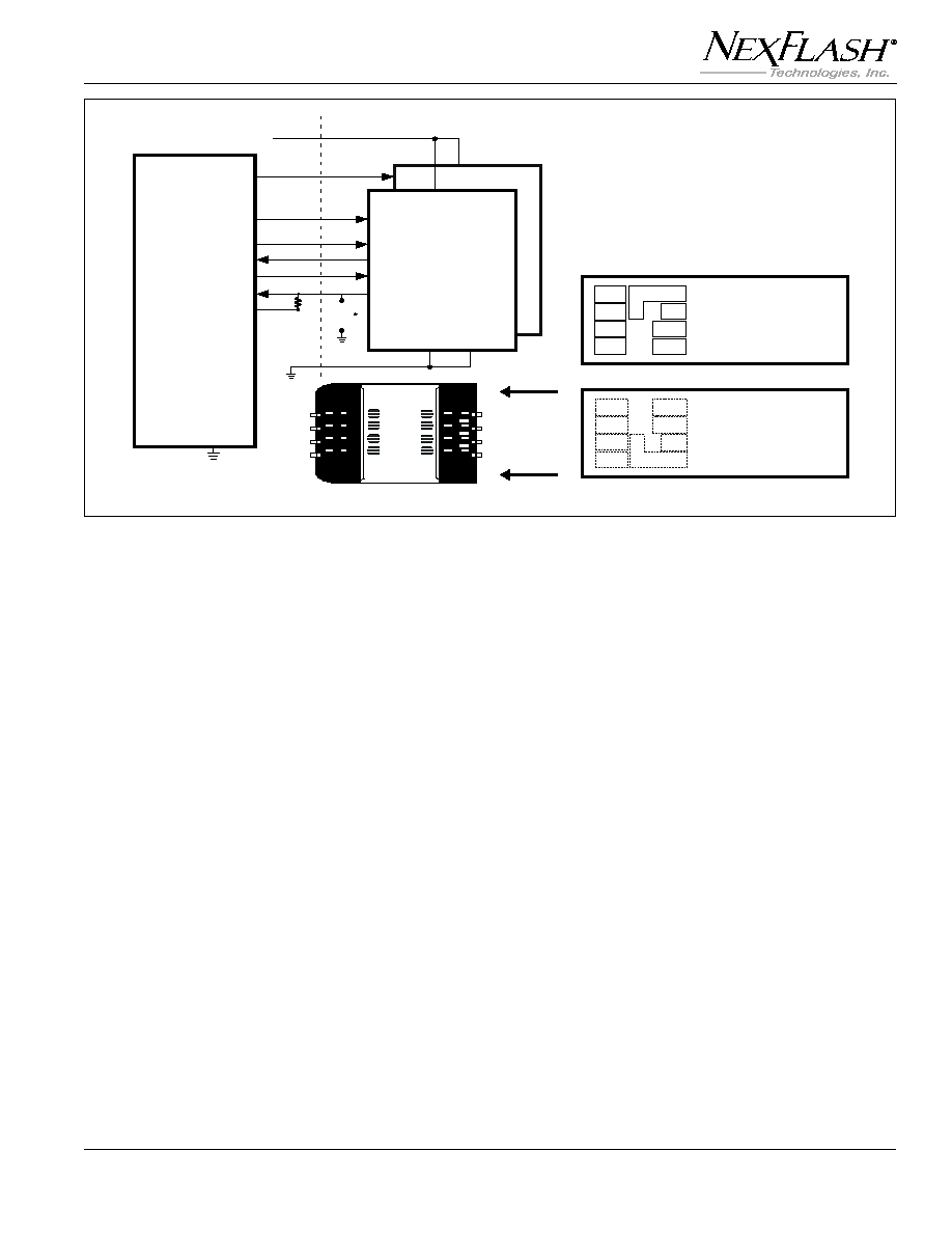
MICROCONTROLLER
(DSP or ASIC)
Vcc
WPS
10K
(2)
(3)
(13)
(12)
(14)
(1)
CS0
SCK
CS1
Vcc
SI
SO
WP/DT
GND
CSO
SCK
CS1
Vcc
Vcc
CS1
SCK
CSO
C1
C2
C4
C3
C7
C8
C6
C5
C1
DT
C4
C8
C3
C7
C6
C2
C5
GND
WP/DT
SO
SI
TOP VIEW
(LABEL SIDE)
DT
C1
C5
C2
C8
C6
C3
C7
C4
GND
WP/DT
SO
SI
BOTTOM VIEW
(CONTACT SIDE)
Vcc
#1
GND
SCK
SO
SI
WP/DT
CS0
CS1
#0
R/
B Hold*
R/
B
Hold
(4)
(1)
Serial Flash
Memory
SPI Interface
25Fxxx Series
CS1*
CS0
SCK
SO
SI
WP/DT
Detect Control*
(11)
(11)
* OPTIONAL
NXD011A-0598
Figure 2. Typical interface for Serial Flash Module with SPI Interface using NX25Fxxx Series Devices.
Equivalent pin numbers for TSOP (Type II) are listed in parentheses. SPI contact assignments are shown for Bottom
and Top Views of Serial Flash Module and Top View of the ITT Cannon Slide-insertion Connector (Model CCM-03-3504).
PIN DESCRIPTIONS
SPI NX25Fxxx Series
Note: See NX25Fxxx Data Sheets for further information
Power Supply Pins (Vcc and Gnd)
Supply source for 5V or 3V. Contact layout allows for the
module to be inserted and removed while power is applied
("hot-socketing") without damaging the module's memory
device.
Serial Data Input (SI)
The SPI bus Serial Data Input (SI) provides a means for
commands or data to be written to (shifted into) the device.
Serial Data Output (SO)
The SPI bus Serial Data Output (SO) provides a means for
data to be read from (shifted out of) the device. When the
device is deselected (
CS=1) SO pin is in a high-impedance
state.
Serial Clock (SCK)
All commands and data written to the Serial Input (SI) are
clocked relative to the rising edge of Serial Clock (SCK). All
data read from the Serial Data Output (SO) is clocked
relative to the falling edge of SCK.
Chip Selects (
CS0
CS0
CS0
CS0
CS0 and CS1
CS1
CS1
CS1
CS1)
CS0 selects device location 0, which is on the contact side
of the module.
CS1 selects device location 1, which is
located on the opposite side of module from device #0.
CS1
is only used when a module has two serial flash memories.
Chip select inputs are asserted low.
Write Protect/Detect (
WP
WP
WP
WP
WP/DT)
The Write Protect/Detect pin is an optional dual function pin.
Write Protect (
WP
WP
WP
WP
WP)
Used as a Write Protect Input (
WP), when WP is asserted
(active low) the entire flash memory array is Write Pro-
tected.
WP can be controlled by the interface or as an
optionally available contact pad directly on the module.
Detect (DT)
Using a pull-up resistor, a card detect (DT) can provide a
low to high or high to low transition when the module is
inserted or removed. The pulse is best used in conjunction
with an interrupt input of a microcontroller or processor.
R/B
Hold
Hold
Hold
Hold
Hold
The Ready/Busy-Hold pin function is not available for use
with the SFM. This pin must be set to "No Connect" in the
NX25Fxxx configuration register.
1
2
3
4
5
6
7
8
9
10
11
12
NexFlash Technologies, Inc.
3
PRELIMINARY
NXSF012B-0599
02/22/00 ©
NX25Mxxx
NX26Mxxx
PIN DESCRIPTIONS
NXS NX26Fxxx Series
Note: See NX26Fxxx Data Sheets for further information
Power Supply Pins (Vcc and Gnd)
Supply source for 5 or 3.0V. Contact layout allows for the
module to be inserted and removed while power is applied
("hot-socketing") without damaging the module's memory
device.
Serial Data Input/Output (SIO)
The NXS bus Serial Data Input/Output (SIO) provides a
means for commands or data to be written to (shifted into)
the device or read from (shifted out of) the device. When the
device is deselected SIO pin is in a high-impedance state.
Serial Clock (SCK)
All commands and data written to the Serial Input (SI) are
clocked relative to the rising edge of Serial Clock (SCK). All
data read from the Serial Data Output (SO) is clocked
relative to the falling edge of SCK.
Device Address Pins (A0, A1, A2, A3)
There is no separate chip select signal for the NXS inter-
face (NX26Fxxx series), instead four static address signals
(A0, A1, A2, and A3) are provided for decoding one of 16
possible addresses. The A0 address signal, which is not
MICROCONTROLLER
(DSP or ASIC)
Vcc
WPS
10K
(2)
(3)
(13)
(12)
(14)
(1)
A3-0
SCK
A3-1
Vcc
A1
SIO
A2 &
WP/DT
GND
A3-0
SCK
A3-1
Vcc
Vcc
A3-1
SCK
A3-0
C1
C2
C4
C3
C7
C8
C6
C5
C1
DT
C4
C8
C3
C7
C6
C2
C5
GND
A2 &
WP/DT
SIO
A1
TOP VIEW
(LABEL SIDE)
DT
C1
C5
C2
C8
C6
C3
C7
C4
GND
A2 &
WP/DT
SIO
A1
BOTTOM VIEW
(CONTACT SIDE)
Vcc
#1
GND
A3
SCK
SIO
A1
A2
A3
#0
A0
A0
(4)
(1)
Serial Flash
Memory
NXS Interface
26Fxxx Series
A3-1*
A3-0
SCK
SIO
A1
A2,
WP/DT
Detect Control*
(11)
(11)
SERIAL I/O,
AND GENERAL
PURPOSE
PORT PINS
* OPTIONAL
NXD012A-0598
Figure 3. Typical interface for Serial Flash Module with NXS Interface using NX26Fxxx Series Devices.
Equivalent pin numbers for TSOP (Type II) are listed in parentheses. NXS contact assignments are shown for Bottom
and Top Views of Serial Flash Module and Top View of the ITT Cannon Slide-insertion Connector (Model CCM-03-3504).
available on the contact pad, is tied low for device #0 (on the
contact side) and is tied high for device #1 (optionally used on
the top side). A1, A2, A3-0, and A3-1, which are available on
the contact pad, must be tied high or low at the connector
according to the desired address of device #0 or #1.
Write Protect/Detect (
WP
WP
WP
WP
WP/DT)
The Write Protect/Detect pin is an optional dual function pin.
Write Protect (
WP
WP
WP
WP
WP)
Write Protect Input (
WP) can be used as a status indicator
for the firmware to determine if a write protect condition
exists on the SFM (if optional
WP switch or contact pad is
available on the SFM). Unlike the NX25Fxxx SPI series the
low on
WP does not provide a direct electrical protection of
the device. Note that this pin also serves as the A2 address.
If used for write protect status the change in device address
must be taken into consideration.
Detect (DT)
Using a pull-up resistor, a card detect (DT) can provide a
low-to-high or high-to-low transition when the module is
inserted or removed. The pulse is best used in conjunction
with an interrupt input of a microcontroller or processor. Note
that this pin also serves as the A2 address. If used for detect
status the device address must be taken into consideration.

NX25Mxxx
NX26Mxxx
4
NexFlash Technologies, Inc.
PRELIMINARY
NXSF012B-0599
02/22/00 ©
OPTIONAL DUAL
CHIP DEVICE
OPTIONAL DUAL
CHIP DEVICE
TOLERANCES:
X.X
[X.XX]
= ±0.3
[±0.012]
X.XX X
[X.XXX] = ±0.1
[±0.004]
15.00 [0.591]
5.00 [0.20]
1.00
[0.040]
RADIUS 0.50 [0.020]
1.50 [0.060]
45.00 [1.772]
2.00 [0.079] MIN
23.00 [0.906] MAX
2.59 [0.102]
1.76 [0.069]
14.75 [0.581]
3.00 [0.118]
3.00 [0.118]
0.76±0.08
[0.030±0.003]
6.0 [0.24]
1.00 [0.039] MIN
3.20 [0.126] MAX
2.00 [0.079] MAX
RADIUS 0.8 [0.03] 3PLCS
NXD013A-0398
Figure 4. Serial Flash Module Package Dimensions TSOP with epoxy version
(Inches are in parentheses)
OPTIONAL DUAL
CHIP DEVICE
OPTIONAL DUAL
CHIP DEVICE
TOLERANCES:
X.X
[X.XX]
= ±0.3
[±0.012]
X.XX X
[X.XXX] = ±0.1
[±0.004]
15.00 [0.591]
5.00 [0.20]
1.00
[0.040]
RADIUS 0.50 [0.020]
1.50 [0.060]
45.00 [1.772]
2.00 [0.079] MIN
23.00 [0.906] MAX
2.59 [0.102]
1.76 [0.069]
14.75 [0.581]
3.00 [0.118]
3.00 [0.118]
0.76±0.08
[0.030±0.003]
6.0 [0.24]
1.00 [0.039] MIN
3.20 [0.126] MAX
2.00 [0.079] MAX
RADIUS 0.8 [0.03] 3PLCS
NXD013A-0398
Figure 5. Serial Flash Module Package Dimensions COB with epoxy version
(Inches are in parentheses)

1
2
3
4
5
6
7
8
9
10
11
12
NexFlash Technologies, Inc.
5
PRELIMINARY
NXSF012B-0599
02/22/00 ©
NX25Mxxx
NX26Mxxx
ABSOLUTE MAXIMUM RATINGS
(1, 2)
Symbol
Parameter
Conditions
Range
Unit
Vcc
Supply Voltage
0 to 7.0
V
V
IN
, V
OUT
Voltage Applied to Any Pin
Relative to Ground
≠0.5 to V
CC
+ 0.5
V
EDC
Electro-static Discharge: Contact
JEIDA 4.1 Specification
±7,000
V
to Insulating or Conductive Plate.
(Non A version devices)
JEIDA 4.1 Specification
±8,000
V
(A version devices)
EDA
Electro-static Discharge: Air Discharge
IEC-1000-4-2 Specification
±7,000
V
to Insulating or Conductive Plate.
(Non A version devices)
IEC-1000-4-2 Specification
±8,000
V
(A version devices)
T
ST
Storage Temperature
≠40 to +85
∞C
Note:
1. This device has been designed and tested for the specified operation ranges. Proper operation outside of these levels is not
guaranteed. Exposure beyond absolute maximum ratings (listed above) may cause permanent damage.
2. Proper care and handling of the Serial Flash Module is mandatory to ensure reliable operation. Avoid bending or subjecting the
module to sudden impact. Avoid directly touching the connectors to protect from damage caused by static discharge.
NexFlash
cannot accept and hereby disclaims liability for any damage to the modules, including data corruption that may occur due to
mishandling.
OPERATING RANGES
Symbol
Parameter
Conditions
Min
Typ
Max
Unit
V
CC
Supply Voltage for Reading and
See specific Serial Flash memory data sheet for 5V or 3V
Writing Main Flash Array
operating range.
V
CCDIS
Supply Voltage for Reading Device
DIS Read-only Voltage
2.7
--
5.5
V
Information Sector (DIS) to Identify
Specified Voltage of Module.
T
A
Ambient Temperature, Operating
Commercial
0
--
+55
∞C
Extended
(2)
≠15
--
+70
∞C
Industrial
(2)
≠40
--
+85
∞C
IRO
Mechanical Insertion and
Office Environment
5,000
10,000
--
Cycles
Removal Cycles
(1)
Using ITT Cannon
Connector CCM03-3504
Note:
1. Tested on a sample basis or specified via design or characterization data.
2. Contact NexFlash for availability of extended and industrial grade devices.
AC AND DC ELECTRICAL CHARACTERISTICS
See associated NX25Fxxx or NX26Fxxx Serial Flash Memory Data Sheet

NX25Mxxx
NX26Mxxx
6
NexFlash Technologies, Inc.
PRELIMINARY
NXSF012B-0599
02/22/00 ©
ORDERING INFORMATION
Size
Order Part No.
Package
128K-Byte
NX25M011A-3V-R
SPI, SFM, TSOP (V Type I)
32 RS, 3V
128K-Byte
NX25M011A-5V-R
SPI, SFM, TSOP (V Type I)
32 RS, 5V
128K-Byte
NX26M011A-3V-R
NXS, SFM, TSOP (V Type I)
32 RS, 3V
128K-Byte
NX26M011A-5V-R
NXS, SFM, TSOP (V Type I)
32 RS, 5V
512K-Byte
NX25M041A-3V-R
SPI, SFM, TSOP (V Type I)
32 RS, 3V
512K-Byte
NX25M041A-5V-R
SPI, SFM, TSOP (V Type I)
32 RS, 5V
512K-Byte
NX26M041A-3V-R
NXS, SFM, TSOP (V Type I)
32 RS, 3V
512K-Byte
NX26M041A-5V-R
NXS, SFM, TSOP (T Type I)
32 RS, 5V
1M-Byte
NX25M080A-3T-R
SPI, SFM, TSOP (T Type II)
64 RS, 3V
1M-Byte
NX25M080A-5T-R
SPI, SFM, TSOP (T Type II)
64 RS, 5V
1M-Byte
NX26M080A-3T-R
NXS, SFM, TSOP (T Type II)
64 RS, 3V
1M-Byte
NX26M080A-5T-R
NXS, SFM, TSOP (T Type II)
64 RS, 5V
2M-Byte
NX25M080A-3T2-R
SPI, SFM, Dual TSOP (T Type II)
64 RS, 3V
2M-Byte
NX25M080A-5T2-R
SPI, SFM, Dual TSOP (T Type II)
64 RS, 5V
2M-Byte
NX26M080A-3T2-R
NXS, SFM, Dual TSOP (T Type II)
64 RS, 3V
2M-Byte
NX26M080A-5T2-R
NXS, SFM, Dual TSOP (T Type II)
64 RS, 5V
2M-Byte
NX26M160-3T-R
NXS, SFM, TSOP (T Type II)
64 RS, 3.0-3.6V
2M-Byte
NX26M160-3C-R
NXS, SFM, COB (T Type II)
64 RS, 3.0-3.6V
2M-Byte
NX26M160-5T-R
NXS, SFM, TSOP (T Type II)
64 RS, 5V
2M-Byte
NX26M160-5C-R
NXS, SFM, COB (T Type II)
64 RS, 5V
4M-Byte
NX26M160-3T2-R
NXS, SFM, Dual TSOP (T Type II)
64 RS, 3.0-3.6V
4M-Byte
NX26M160-3C2-R
NXS, SFM, Dual COB (T Type II)
64 RS, 3.0-3.6V
4M-Byte
NX26M160-5T2-R
NXS, SFM, Dual TSOP (T Type II)
64 RS, 5V
4M-Byte
NX26M160-5C2-R
NXS, SFM, Dual COB (T Type II)
64 RS, 5V
Note: To order SFM's without labels contact
NexFlash's Serial Flash Marketing Department.

1
2
3
4
5
6
7
8
9
10
11
12
NexFlash Technologies, Inc.
7
PRELIMINARY
NXSF012B-0599
02/22/00 ©
NX25Mxxx
NX26Mxxx
PRELIMINARY DESIGNATION
The "Preliminary" designation on an
NexFlash data sheet
indicates that the product is not fully characterized. The
specifications are subject to change and are not guaran-
teed.
NexFlash or an authorized sales representative
should be consulted for current information before using
this product.
IMPORTANT NOTICE
NexFlash reserves the right to make changes to the
products contained in this publication in order to improve
design, performance or reliability.
NexFlash assumes no
responsibility for the use of any circuits described herein,
conveys no license under any patent or other right, and
makes no representation that the circuits are free of
patent infringement. Charts and schedules contained
herein reflect representative operating parameters, and
may vary depending upon a user's specific application.
While the information in this publication has been
carefully checked,
NexFlash shall not be liable for any
damages arising as a result of any error or omission.
LIFE SUPPORT POLICY
NexFlash does not recommend the use of any of its
products in life support applications where the failure or
malfunction of the product can reasonably be expected to
cause failure in the life support system or to significantly
affect its safety or effectiveness. Products are not autho-
rized for use in such applications unless
NexFlash receives
written assurances, to its satisfaction, that:
(a) the risk of injury or damage has been minimized;
(b) the user assumes all such risks; and
(c) potential liability of
NexFlash is adequately protected
under the circumstances.
Trademarks:
NexFlash is a trademark of NexFlash Technologies, Inc. All
other marks are the property of their respective owner.