
NexFlash Technologies, Inc.
1
PRELIMINARY
NXSF006E-0801
08/22/01 ©
NX26F080A
NX26F160
8M-BIT AND 16M-BIT SERIAL FLASH MEMORY
WITH 2-PIN NXS INTERFACE
FEATURES
∑ Tailored for Portable and Mobile Media-Storage
≠ Ideal for portable/mobile applications that transfer
and store data, audio, or images
≠ Removable Serial Flash Module package option
∑
NexFlash TM Non-volatile Memory Technology
≠ Patented Single-Transistor EEPROM Cell
≠ High-density, cost-effective, low-voltage/power
≠ 10K/100K endurance, ten years data retention
∑ Flash Memory for Battery-Operation
≠ Single 5V or 3V supply for Read, Erase/Write
≠ Icc 15 mA active with 1
µA standby power
≠ 5 ms Erase/Write times for efficient battery use
∑ 8M-bits or 16M-bits of
NexFlash Serial Memory
≠ 2,048 or 4,096 sectors of 536 bytes each
≠ Simple commands: Reset, Read, Write,
Ready/Busy
≠ No pre-erase required, auto-erases before write
∑ Two-pin NXS Serial Interface
≠ Saves Microcontroller-pins, simplifies PCB layout,
low switching noise compared to parallel Flash
≠ Supports clock operation as fast as 16 MHz
≠ Multi-device cascading, up to 16 devices
∑ Development Tools and Accessories
≠ NX-SFK-NXS Serial Flash Development Kit
Description
The
NexFlashTM NX26F080A and NX26F160 Serial Flash
Memories are tailored for portable/mobile media-storage
applications that transfer and store data, audio and images.
Manufactured using
NexFlash's patented single transistor
EEPROM memory cell, the NX26F080A and NX26F160
provide a high-density, low-voltage, low-power, and cost
effective solution for battery-operated nonvolatile data stor-
age requirements. The NX26F080A and NX26F160 can
operate with a single 5V or 3V supply for Read, Write, and
Erase. Power consumption is very low due to
µA standby
current and fast Erase/Write performance (as fast as 5 ms
per sector) that minimizes power-on time, resulting in a
highly efficient energy-per-transfer ratio. The NX26F080A
PRELIMINARY
AUGUST 1999
and NX26F160 offer 8M-bits and 16M-bits of Flash memory
organized in sectors of 536 bytes each. Each sector is
individually addressable through basic commands or con-
trol functions such as Reset, Read, Erase/Write, and
Ready/Busy. The NXS (
NexFlash Serial) 2-wire serial
interface is ideal for use with microcontrollers since it only
requires two pins. This leaves pins normally used for parallel
Flash free for other uses. The NXS interface supports clock
rates as fast as 16 MHz and allows for multi-device cascading
of up to 16 devices. It also simplifies PC-board layout and
generates less transient noise than parallel devices. Devel-
opment is supported with the NexFlash Serial Flash
Development Kit.
This document contains PRELIMINARY INFORMATION. NexFlash reserves the right to make changes to its product at any time without notice in order to improve design and supply the
best possible product. We assume no responsibility for any errors which may appear in this publication.
Copyright 1998, NexFlash Technologies, Inc.
NX26F080A
NX26F160
2
NexFlash Technologies, Inc.
PRELIMINARY
NXSF006E-0801
08/22/01 ©
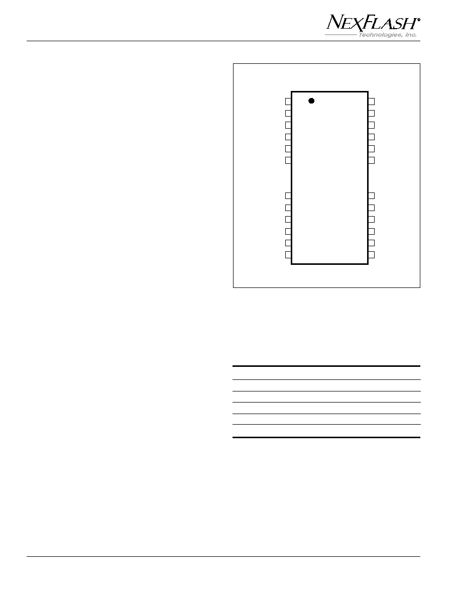
Pin Descriptions
Package Types
The NX26F080A and NX26F160 is available in a 24/28-pin
TSOP (Type II) package (Figure 1 and Table 1) or a
removable Serial Flash Module (see NX25Mxxx/NX26Mxxx
Serial Flash Module data sheet for further information).
Power Supply Pins (Vcc and GND)
The NX26F080A and NX26F160 support single power supply
Read, Erase, and Write operations available in 5V and 3V Vcc
versions. Active power requirements are as low as 15 mA for
3V versions with standby current in the 1
µA range.
NXS Serial Interface Pins (SCK and SIO)
The 2-wire NXS (NexFlash Serial) interface includes a
Clock Input pin (SCK) and a single bidirectional I/O pin for
data (SIO). All data to or from the SIO pin is clocked
relative to the rising edge of SCK. The 2-wire NXS serial
interface makes the NX26F080A and NX26F160 an ideal
solution for removable non-volatile storage. A simple edge
connector or cable/connector with four contacts (SCK,
SIO, Vcc, and GND) can support communications with
space efficiency and reliability. The NXS interface can
operate at clock rates up to 16 MHz for 5V versions.
Device Address Pins (A0, A1, A2, A3)
There is no active chip select on the NX26F080A and
NX26F160. Instead, four static device address pins
(A0, A1, A2, and A3) are provided for decoding from one to
16 possible devices (Figure 2). This allows up to 16MB
(using an NX26F080A device) or 32MB (using an NX26F160
device) to be addressed via a single 2-wire NXS interface.
The static address pins (A0-A3) must be tied high or low to
match the device address field (DA3-DA0) in the sector
Read and Erase/Write instruction sequences.
No Connect Pins (N/C)
The NX26F080A and NX26F160 uses only a few signal
pins. As a result, the TSOP package has numerous
no connects (NC) that have no electrical contact to the die.
Table 1. Pin Descriptions
A0, A1, A2, A3
Device Address
SCK
Serial Clock
SIO
Serial Data I/O
Vcc
Power Supply
GND
Ground
NC
No Connect
A0
SCK
SIO
Vcc
NC
NC
NC
NC
A3
A2
A1
GND
N/C
NC
NC
NC
NC
NC
NC
NC
NC
NC
NC
NC
1
2
3
4
5
6
9
10
11
12
13
14
28
27
26
25
24
23
20
19
18
17
16
15
Figure 1. NX26F080A and NX26F160 Pin Assignments

1
2
3
4
5
6
7
8
9
10
11
12
NexFlash Technologies, Inc.
3
PRELIMINARY
NXSF006E-0801
08/22/01 ©
NX26F080A
NX26F160
....
....
NX26F080A or
NX26F160
U0
NX26F080A or
NX26F160
U8
NX26F080A or
NX26F160
U9
NX26F080A or
NX26F160
U10
NX26F080A or
NX26F160
U11
NX26F080A or
NX26F160
U1
NX26F080A or
NX26F160
U2
NX26F080A or
NX26F160
U3
SCK
SIO
MICROCONTROLLER / MICROPROCESSOR
DSP or ASIC
0
A0
0
A1
0
A2
1
A3
1
A0
0
A1
0
A2
1
A3
0
A0
1
A1
0
A2
1
A3
1
A0
1
A1
0
A2
1
A3
1
A0
1
A1
0
A2
0
A3
0
A0
1
A1
0
A2
0
A3
1
A0
0
A1
0
A2
0
A3
0
A0
0
A1
0
A2
0
A3
Figure 2. NX26F080A or NX26F160 Used in a Multi-device Configuration with up to 16-Devices on the 2-wire NSX
FUNCTIONAL OVERVIEW
The
NexFlash NX26F080A and NX26F160 provide up to
8M-bits or 16M-bits of non-volatile memory organized as
2,048 or 4,096 small sectors of 536 bytes (4,288 bits) each
(Figure 3). Each sector is individually addressable using
basic instruction sequences and control functions commu-
nicated through the devices 2-wire NXS interface.
Read and Erase/Write Instruction Sequences
The NX26F080A and NX26F160 have two basic instruction
sequences: Read and Erase/Write. Unlike some other
Flash technologies, the erase and write operations of the
NX26F080A and NX26F160 are performed together in one
single operation (as fast as 5 ms per sector). Thus,
pre-erase of the memory is not necessary.
Both Read and Erase/Write instructions are made up of a
series of serial bit fields that include command, sector
address, device address, and sector data. The Read
instruction sequence also allows the device to be polled for
Ready/Busy status.
Sector 0 (0000H)
4288 Bits (536 Bytes) Per Sector
Sector 1 (0001H)
Sector 2 (0002H)
Sectors 3-2045/4093
(0003-07FD/0FFDH)
Sector 2046/4094 (07FE/0FFEH)
Sector 2047/4095 (07FF/0FFFH)
Figure 3.
NexFlash's NX26F080A and NX26F160 Array

NX26F080A
NX26F160
4
NexFlash Technologies, Inc.
PRELIMINARY
NXSF006E-0801
08/22/01 ©
The instruction sequence format, flow charts, and clocking
diagrams for Read and Erase/Write operations are shown in
Figures 5 and 6, Figures 7 and 8, and Figures 9 and 10,
respectively. All data within an instruction sequence is
clocked on the rising edge. All instruction sequence fields are
ordered by most significant bit first (MSB). Data is erased and
written to the NX26F160 and NX26F080A memory array a full
sector (536 bytes) at a time. If all 536 bytes of a given sector
are not fully clocked into the device, the remaining byte
locations will be overwritten with indeterminate values. To
ensure the highest level of data integrity write operations
should be verified and rewritten, if needed, (see High Data
Integrity Applications).
Reset and Idle
Upon power-up and between Read and Erase/Write instruc-
tion sequences, the device's internal control logic will be
reset. This is accomplished by asserting the SCK pin low
(to V
IL
) for greater than
t
RESET
. Once reset, the device enters
standby operation and will not wake-up until the next rising
edge of SCK. After an initial rising SCK occurs, the device
becomes ready for a new instruction sequence. Full active
power consumption starts after the correct device address is
decoded during a Read or Write instruction sequence. To idle
an instruction sequence between clocks, SCK must be kept
high (at V
IH
) for as long as needed. Note that power will be in
the active state when SCK is held high.
Device Initialization
After power-up it is recommended that the device information
sector be read to electronically identify the device. The
device information format contains a device ID that identifies
the manufacturer, part number (memory size), and operating
range. It also contains a list of any restricted sectors
(see Sector Tag/Sync bytes). For a further description of the
NX26F080A and NX26F160 device information format, see
the Serial Flash Device Information Sector Application Note
SFAN-02.
As shown in Figure 6, the address for the device information
sector address is at 5000H for both the NX26F080A and
NX26F160. The device information sector is a "read-only"
sector. This assures that all device specific information,
such as the restricted sector list, is maintained and never
written over inadvertently.
For compatibility with applications that used the original
NX26F080 (non A), which does not have a separate device
information sector, a copy of the device information sector is
also provided in the last two sectors of the NX26F080A
(07FFH and 07FEH) and NX26F160 (0FFFH and 0FFEH).
Contact
NexFlash's Serial Flash applications department if
you require compatibility with the NX26F080 (non A).
Ready/Busy Status
After an Erase/Write instruction sequence has been
executed, the device will become Busy while it erases and
writes the addressed sector's memory. This period of time
will not exceed t
WP
(~5 to 30 ms based on the specified power
supply operating voltage). During this time the device can be
tested for a Ready/Busy condition via a 16-bit status value
obtained in the Read instruction sequence. The Busy status
condition (6666H) indicates that the device has not yet
completed its write operation and will not accept read or write
instructions. The Ready status condition (9999H) indicates
that the device is available for further read or write operations.
Note that a delay time of t
RP
(~30 µs to 100 µs depending on
the voltage version being used) is required after the first low
to high clock transition of the Ready/Busy status read.
Sector Tag/Sync Bytes
The first byte of each sector is pre-programmed during
manufacturing with a Tag/Sync value of "C9H". Although the
first byte of each sector can be changed, it is recommended
that Tag/Sync value be maintained and incorporated as part
of the application's sector formatting. The Tag/Sync values
serve two purposes. First, they provide a sync-detect that
can help verify if the instruction sequence was clocked into
the device properly. Secondly, they serve as a tag to identify
a fully functional (valid) sector. This is especially important
if "restricted sector" devices are used.
Restricted sector devices provide a more cost effective
alternative to NX26F080A or NX26F160 devices with 100%
valid sectors. Restricted sector devices have a limited
number of sectors (64 maximum. for the NX26F080A and
NX26F160) that do not meet manufacturing programming
criteria over the specified operating range. When such a
sector is detected, the first byte is tagged with a pattern other
than "C9H". In addition to individual sector tagging, all
restricted sectors for a given device are listed in the "device
information format" (see Device Initialization).
High Data Integrity Applications
Data storage applications that use Flash memory or other
non-volatile media must take into consideration the possibil-
ity of noise or other adverse system conditions that may
affect data integrity. For those applications that require higher
levels of data integrity it is a recommended practice to use
Error Correcting Code (ECC) techniques. The NexFlash
Serial Flash Development Kit provides a software routine for
a 32-bit ECC that can detect up to two bit errors and correct
one. The ECC not only minimizes problems caused by
system noise but can also extend Flash memory endurance.
For those systems without the processing power to handle
ECC algorithms, a simple "verification after write" is recom-
mended. The NexFlash Serial Flash Development Kit
software includes a simple Write/Verify routine that will
compare data written to a given sector and rewrite the sector
if the compare is not correct.

1
2
3
4
5
6
7
8
9
10
11
12
NexFlash Technologies, Inc.
5
PRELIMINARY
NXSF006E-0801
08/22/01 ©
NX26F080A
NX26F160
C3-C0 SA11-0 DA3-0 SA15-12 R31-R0 S15-S0 D0 - - - D4287
INITIAL CLOCK
To wake device from standby
(Data is "Don't Care")
COMMAND TYPE
1H = Read
MAIN SECTOR ADDRESS
000H-7FFH for NX26F080A
000H-FFFH for NX26F160
DEVICE ADDRESS
A0-A3 pins = 0H-FH
AUXILARY SECTOR ADDRESS
0H = To address main sector address 0-FFF
5H = Device information sector
RESERVED
Use 00 00 00 00H for
NX26F080A and NX26F160
INPUT STATUS BYTES
9999H = Ready, 6666H = Busy
Note: Delay is required during
status byte read, see
t
RP
in
AC Characteristics
INPUT SECTOR DATA BITS
(536 Bytes)
Command
Address
Reserved
Status
Data
Figure 5. Sector Read Instruction - Sequence and Bit Instruction

NX26F080A
NX26F160
6
NexFlash Technologies, Inc.
PRELIMINARY
NXSF006E-0801
08/22/01 ©
INITIAL CLOCK
To wake device from standby
(Data is "Don't Care")
COMMAND TYPE
2H = Write
MAIN SECTOR ADDRESS
000H-7FFH for NX26F080A
000H-FFFH for NX26F160
DEVICE ADDRESS
A0-A3 pins = 0H-FH
AUXILARY SECTOR ADDRESS
0H = main sector address 0-FFF
RESERVED
Use 00 00 00 00H for
NX26F080A and NX26F160
SECTOR DATA BITS
0-4287 (536 Bytes)
16 EXTRA CLOCKS
(Data is "Don't Care")
C3-C0 SA11-0
DA3-0 A15-12 R31-R0 D0 - - - D4287 X15-X0
Control
Data
Reserved
Address
Command
Figure 6. Sector Erase/Write Instruction - Sequence and Bit Format

1
2
3
4
5
6
7
8
9
10
11
12
NexFlash Technologies, Inc.
7
PRELIMINARY
NXSF006E-0801
08/22/01 ©
NX26F080A
NX26F160
Output remaining 535 bytes
(4280 bits) of sector data
Output (Rewrite )1st byte of sector
with C9H Tag/Sync bite
Output two bytes of zeros (00 00H)
for the IS26F160
Assert CLK low for
t
RESET
to invoke Erase/Write Operation
and then standby operation
Output one clock to wake
device from stand-by
Call Read Sector Routine to
check Ready/Busy and Tag
Start Sector Erase/Write Routine
Return
(1)
Yes
No*
Device
Ready and Sector
Tag valid
*Set Flag and process
accordingly upon return
Output Command Sequence:
-Read command C3-C0 (0002B)
-Main Sector Address SA11-0
(000-FFFH)
-Device Address DA3-DA0
(per state of A3, A2, A1, A0 pins)
-Auxilary Address A15-A12
0H for main array
-Four reserved bytes R31-R0
(00 00 00 00H)
Figure 8. Sector Erase/Write Operation Flow Chart
Input first byte of data
(Tag/Sync) from sector
*Set Flag and process
accordingly upon return
Return
Yes
No*
No*
Yes*
Ready?
(99 99H)
Input remaining 535 bytes of
sector data (4280 bits)
Return to write routine?
Assert CLK low for
t
RESET
to
reset device and invoke standby
Valid Sector?
(C9H)
No
Start Sector Read Routine
Output clock (low to high) to
wake device from standby
Input Ready/Busy Status S15-S0.
Note t
RP
delay time is
required during status read
(See AC Timing and Figure 10)
Output Command Sequence:
-Read command C3-C0 (0001B)
-Main Sector Address SA11-0
(000-FFFH)
-Device Address DA3-DA0
(per state of A3, A2, A1, A0 pins)
-Auxilary Address A15-A12
0H for main array
5H device information sector
-Four reserved bytes R31-R0
(00 00 00 00H)
Yes
Figure 7. Sector Read Operation Flow Chart
Note:
1. To ensure higher data integrity verify each sector write with a sector read. See High Data Integrity Applications on Page 4.
NX26F080A
NX26F160
8
NexFlash Technologies, Inc.
PRELIMINARY
NXSF006E-0801
08/22/01 ©
Device leaves standby mode at this edge
Read
Command
12-Bit Sector Address
Float SIO so data direction can change from device input to output
Status Word (S15-S0): Ready: 9999H or Busy:6666H
Device Releases SIO Line
Device Drives SIO Line
t
RESET
8 Clocks
4280 Clocks
Device
Address
Aux.
Address
Bytes 0 to 534
Bytes 0 to 535
Four Reserved Bytes (Use 00 00 00 00H)
0
0
0
1
A11 A10 A9 A8
A7
A6
A5
A4
A3
A2
A1
A0 DA3 DA2 DA1 DA0 A15 A14 A13 A12
SCK
SIO
SCK
SIO
SCK
SIO
SCK
SIO
t
RP
1
0
0
1
1
0
0
1
1
0
0
1
1
0
0
1
MSB
LSB
Figure 9. Read Instruction Sequence Clocking

1
2
3
4
5
6
7
8
9
10
11
12
NexFlash Technologies, Inc.
9
PRELIMINARY
NXSF006E-0801
08/22/01 ©
NX26F080A
NX26F160
Device leaves standby mode at this edge
Device enters standby mode after
t
WP
Write
Command
12-Bit Sector Address
Device
Address
0H
Four reserved bytes (use 00 00 00 00H)
MSB
LSB
Byte 1
Byte 0
Bytes 2 to 533
8 Clocks
4256 Clocks
8 Clocks
8 Clocks
16 Extra Clocks
8 Clocks
Byte 535
Byte 534
t
RESET
Don't Care
t
WP
SCK
SIO
SCK
SIO
SCK
SIO
SCK
SIO
0
0
1
0
A11 A10 A9
A8
A7
A6
A5
A4
A3
A2
A1
A0 DA3 DA2 DA1 DA0
0
0
0
0
Figure 10. Erase/Write Instruction Sequence Clocking
NX26F080A
NX26F160
10
NexFlash Technologies, Inc.
PRELIMINARY
NXSF006E-0801
08/22/01 ©
ABSOLUTE MAXIMUM RATINGS
(1)
Symbol
Parameter
Conditions
Range
Unit
Vcc
Supply Voltage
0 to 7.0
V
V
IN
, V
OUT
Voltage Applied to Any Pin
Relative to Ground
≠0.5 to Vcc + 0.6
V
T
STG
Storage Temperature
≠65 to +150
∞
C
T
LEAD
Lead Temperature
Soldering, Ten Seconds
+300
∞
C
Note:
1. This device has been designed and tested for the specified operation ranges. Proper operation outside of these levels is not
guaranteed. Exposure beyond absolute maximum ratings (listed above) may cause permanent damage
OPERATING RANGES
Symbol
Parameter
Conditions
Min
Max
Unit
Vcc
Supply Voltage
26F080A-5T-R
26M080A-5T-R
4.5
5.5
V
26F080A-3T-R
26M080A-3T-R
2.7
3.6
V
26F160-5T-R
26M160-5T-R
4.5
5.5
V
26F160-3T-RS1
26M160-3T-R
3.0
3.6
V
26F160-3T-R
2.85
3.6
V
T
A
Ambient Temperature,
Commercial
0
+70
∞C
Operating
Extended
(1)
≠15
+80
∞C
Industrial
(1)
≠40
+85
∞C
Note:
1. Contact
NexFlash for availability of extended or industrial grade devices.
DC ELECTRICAL CHARACTERISTICS
Symbol
Parameter
Conditions
Min
Typ
Max
Unit
V
IL
Input Low Voltage
≠0.4
--
V c c x 0 . 2
V
V
IH
Input High Voltage
V c c x 0 . 6
--
Vcc + 0.5
V
V
OL
Output Low Voltage
I
O L
= 2 mA, V
C C
= 4.5V
--
--
0.45
V
V
OH
Output High Voltage
I
O H
= ≠400
µA, V
C C
= 4.5V
2.4
--
--
V
V
OLC
Output Low Voltage CMOS
(1)
V
C C
= Min, I
O L
= 10
µA
--
--
0.15
V
V
OHC
Output High Voltage CMOS
(1)
V
C C
= Min, I
O H
= ≠10
µA
V
C C
≠ 0.3
--
--
V
I
L I
Input Leakage
0 < V
I N
< V c c
≠10
--
+10
µA
I
OL
I/O Leakage
0 < V
I N
< Vcc, Output Disabled
≠10
--
+10
µA
I
C C
(active)
Active Power Supply Current
(2)
f
C L K
8 MHz (1/t
C P
)
V
C C
= 4.5V to 5.5V
--
15
30
mA
V
C C
= 2.7V to 3.6V (NX26F080A)
--
5
10
V
C C
= 2.85V to 3.6V (NX26F160)
--
10
20
I
C C S B
(standby) Standby Power Supply Current
SIO = 0V or V
C C
,
--
<1
10
µA
SCK = 0V
C
IN
Input Capacitance
(1)
T
A
= 25∞C, V
C C
= 5V or 3V
--
--
10
pF
Frequency = 1 MHz
C
OUT
Output Capacitance
(1)
T
A
= 25∞C, V
C C
= 5V or 3V
--
--
10
pF
Frequency = 1 MHz
Notes:
1. Tested on a sample basis or specified via design or characterization data.
2. The device leaves "standby" power consumption after the clock transitions from low-to-high. Full "active" power consumption
starts after the correct device address has been decoded during a sector read or write sequence.

1
2
3
4
5
6
7
8
9
10
11
12
NexFlash Technologies, Inc.
11
PRELIMINARY
NXSF006E-0801
08/22/01 ©
NX26F080A
NX26F160
AC ELECTRICAL CHARACTERISTICS
5V (16 MHz)
3V (8 MHz)
Symbol
Description
Min
Typ
Max
Min
Typ Max
Unit
t
CP
SCK Serial Clock Period
62
--
--
125
--
--
ns
t
CL
, t
CH
SCK Serial Clock High or Low Time
26
--
--
57
--
--
ns
t
CR
SCK Serial Clock Rise Time
(1)
--
--
7
--
--
5
ns
t
CF
SCK Serial Clock Fall Time
(1)
--
--
7
--
--
5
ns
t
DS
SIO Setup Time to SCK Rising Edge
40
--
--
100
--
--
ns
t
DH
SIO Hold Time From SCK Rising Edge
0
--
--
0
--
--
ns
t
DV
SIO Valid after SCK
(2)
--
--
60
--
--
115
ns
t
RESET
SCK Low Duration for
1
--
5
2
--
1 0
µs
Valid Reset or Standby
(See Figures 9 & 10)
t
RP
Read Pre-data Delay
(See Figure 9)
3 0
--
--
1 0 0
--
--
µs
t
WP
Erase/Write Program Time
(3)
N X 2 6 F 0 8 0 A
--
3
5
--
5
1 0
m s
(See Figure 10)
N X 2 6 F 1 6 0
--
4
5 . 5
--
2 5
3 2
Notes:
1. Test points are 10% and 90% points for rise/fall times. All other timings are measured at the 50% point.
2. With 50 pF (8 MHz) or 30 pF (16 MHz) load SIO to GND.
3. The NX26F080A and NX26F160 are designed for Erase/Write endurances of 10K cycles. Endurance in the range of 100K
cycles can be obtained using ECC software methods like those provided in the SFK Serial Flash Development Kit.
SCK
SIO
Read
Write
t
CP
t
CH
t
CL
t
DS
t
DH
t
CF
t
CR
t
DV
t
DV
CLOCK AND DATA TIMING
NX26F080A
NX26F160
12
NexFlash Technologies, Inc.
PRELIMINARY
NXSF006E-0801
08/22/01 ©
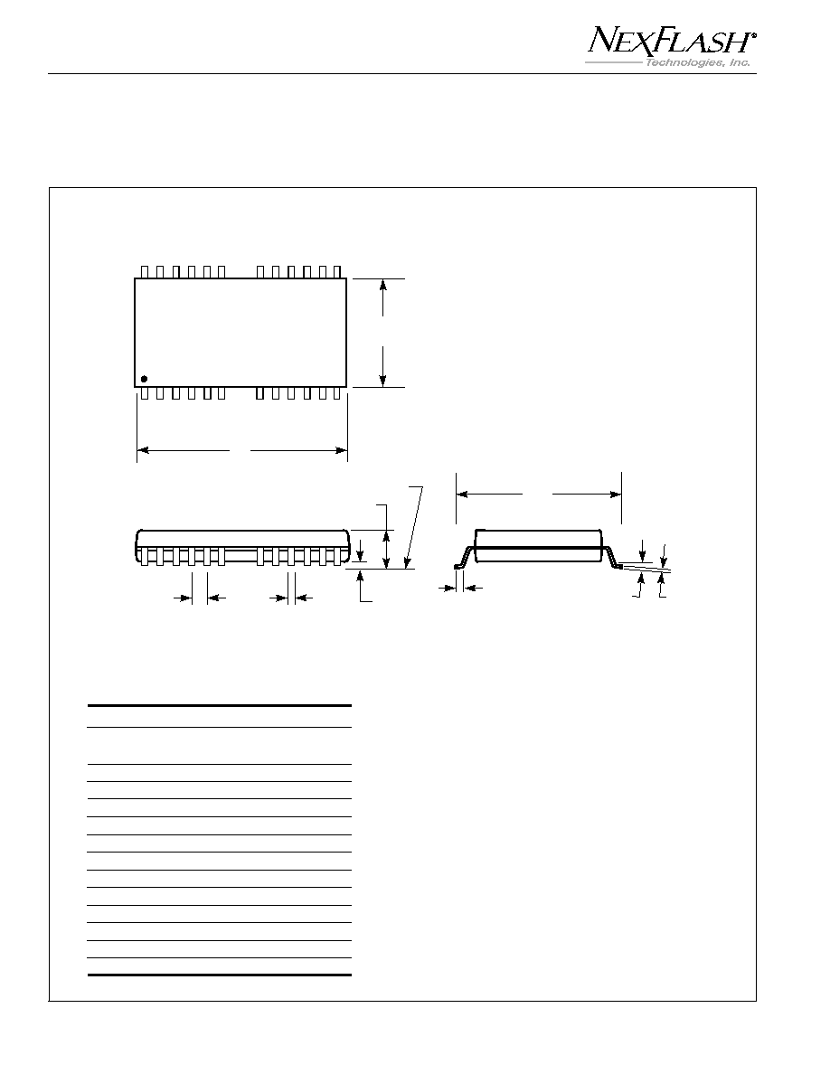
PACKAGE INFORMATION
Plastic TSOP - 24/28-pins
Package Code: T (Type II)
Notes:
1. Controlling dimension: millimeters, unless
otherwise specified.
2. BSC = Basic lead spacing between centers.
3. Dimensions D and E1 do not include mold
flash protrusions and should be measured
from the bottom of the package.
4. Formed leads shall be planar with respect
to one another within 0.004 inches at the
seating plane.
Plastic TSOP (T--Type II)
Millimeters
Inches
Symbol
Min
Max
Min
Max
Ref. Std.
No. Leads
24/28
A
1.00
1.20
0.039
0.047
A1
0.05
0.20
0.002
0.008
B
0.36
0.51
0.014
0.020
C
0.10
0.20
0.004
0.008
D
18.31
18.52
0.721
0.729
E
10.06
10.26
0.396
0.404
H
11.74
11.94
0.462
0.047
e
1.27 BSC
0.050 BSC
L
0.43
0.584
0.017
0.023
0∞
5∞
0∞
5∞
D
SEATING PLANE
B
e
C
1
N/2
N/2+1
N
E
H
A1
A
L
1
2
3
4
5
6
7
8
9
10
11
12
NexFlash Technologies, Inc.
13
PRELIMINARY
NXSF006E-0801
08/22/01 ©
NX26F080A
NX26F160
ORDERING INFORMATION
Size
Order Part No.
Package/Description
(2)
8M-bit
NX26F080A-3T-R
(1)
NXS, 28-pin, TSOP (Type II)
64 RS, 3V Low Voltage
8M-bit
NX26F080A-5T-R
(1)
NXS, 28-pin, TSOP (Type II)
64 RS, 5V Standard Voltage
16M-bit
NX26F160-3T-R
NXS, 28-pin, TSOP (Type II)
64 RS, 2.85V-3.6V Low Voltage
16M-bit
NX26F160-3T-RS1
NXS 28-pin, TSOP (Type II)
64 RS 3.0V-3.6V Low Voltage
16M-bit
NX26F160-5T-R
(1)
NXS, 28-pin, TSOP (Type II)
64 RS, 5V Standard Voltage
Notes:
1. Add E (Extended) or I (Industrial) after package designator (T) for alternative
temperature grades.
2. See 26Mxxx data sheet for Serial Flash Module package.
PRELIMINARY DESIGNATION
The "Preliminary" designation on an
NexFlash data sheet
indicates that the product is not fully characterized. The
specifications are subject to change and are not guaran-
teed.
NexFlash or an authorized sales representative should
be consulted for current information before using this
product.
IMPORTANT NOTICE
NexFlash reserves the right to make changes to the
products contained in this publication in order to improve
design, performance or reliability.
NexFlash assumes no
responsibility for the use of any circuits described herein,
conveys no license under any patent or other right, and
makes no representation that the circuits are free of patent
infringement. Charts and schedules contained herein
reflect representative operating parameters, and may vary
depending upon a user's specific application. While the
information in this publication has been carefully checked,
NexFlash shall not be liable for any damages arising as a
result of any error or omission.
LIFE SUPPORT POLICY
NexFlash does not recommend the use of any of its
products in life support applications where the failure or
malfunction of the product can reasonably be expected to
cause failure in the life support system or to significantly
affect its safety or effectiveness. Products are not autho-
rized for use in such applications unless
NexFlash receives
written assurances, to its satisfaction, that:
(a) the risk of injury or damage has been minimized;
(b) the user assumes all such risks; and
(c) potential liability of
NexFlash is adequately protected
under the circumstances.
Trademarks:
NexFlash
TM
is a trademark of
NexFlash Technologies, Inc.
All other marks are the property of their respective owners.

NX26F080A
NX26F160
14
NexFlash Technologies, Inc.
PRELIMINARY
NXSF006E-0801
08/22/01 ©