
NexFlash Technologies, Inc.
1
NXPF001G-0403
04/14/03 ©
This document contains PRELIMINARY data. NexFlash reserves the right to make changes to its products at any time without notice in order to improve design and supply the best possible product. We
assume no responsibility for any errors which may appear in this publication. © Copyright 1998, NexFlash Technologies, Inc..
NX29F010
1M-BIT (128K x 8-bit)
CMOS, 5.0V Only
ULTRA-FAST SECTORED FLASH MEMORY
FEATURES
∑ Ultra-fast Performance
≠ 35, 45, 55, 70, and 90 ns max. access times
∑ Temperature Ranges
≠ Commercial 0
o
c-70
o
c
≠ Industrial -40
o
c-85
o
c
∑ Single 5V-only Power Supply
≠ 5V ± 10% for Read, Program, and Erase
∑ CMOS Low Power Consumption
≠ 20 mA (typical) active read current
≠ 30 mA (typical) Program/Erase current
∑ Compatible with JEDEC-Standard Pinouts
≠ 32-pin DIP, PLCC, TSOP
∑ Program/function Compatible with AM29F010
≠ No system firmware changes
≠ Uses same PROM programer algorithm
∑ Flexible sector architecture
≠ Erase any of eight uniform sectors or full chip erase
≠ Sector protection/unprotection using PROM
programming equipment
∑ 100,000 Program/Erase cycles
∑ Embedded algorithms
≠ Automatically programs and verifies data at
specified address
≠ Auto-programs and erases the chip or any
designated sector
∑ Data/Polling and Toggle Bits
≠ Detect program or erase cycle completion
JUNE 2000
DESCRIPTION
The
NexFlash
NX29F010 is a 1 Megabit (131,072 bytes)
single 5.0V-only Sectored Flash Memory. The NX29F010
provides in-system programming with the standard system
5.0V-only Vcc supply and can be programmed or erased in
standard PROM programmers.
The NX29F010 offers access times of 35, 45, 55, 70, and
90 ns allowing high-speed controller and DSPs' to operate
without wait states. Byte-wide data appears on DQ0-DQ7.
Separate chip enable (
CE), write enable (WE), and output
enable (
OE) controls eliminates bus contention.
Power consumption is greatly reduced when the system
places the device into the Standby Mode.
The device is offered in 32-pin PLCC, TSOP, and PDIP
packages.
Principles of Operation
Only a single 5.0V power supply is required for both read and
write functions. Program or erase operations do not require
12.0V V
PP
. Internally generated and regulated voltages are
provided for the program and erase operations.
The device is entirely command set compatible with the
JEDEC single power supply Flash standard. Commands
are written to the command register using standard micro-
processor write timings. Register contents serve as input to
an internal state machine that controls the erase and
programming circuitry. Write cycles also internally latch
addresses and data needed for the programming and
erase operations. Reading data out of the device is similar
to reading from other Flash or EPROM devices.
Executing the Program Command Sequence invokes the
Embedded Program Algorithm, an internal algorithm that
automatically times the program pulse widths and verifies
proper cell margin.
NX29F010
2
NexFlash Technologies, Inc.
NXPF001G-0403
04/14/03 ©
WE
STATE
CONTROL
COMMAND
REGISTER
CE
OE
PGM VOLTAGE
GENERATOR
CHIP ENABLE/
OUTPUT ENABLE
LOGIC
ERASE VOLTAGE
GENERATOR
INPUT/OUTPUT
BUFFERS
DATA
LATCH
STB
STB
Y-DECODER
X-DECODER
ADDRESS LATCH
Y-GATING
CELL
MATRIX
VCC
DETECTOR
TIMER
VCC
GND
A0-A16
DQ7-DQ0
8
8
8
8
8
8
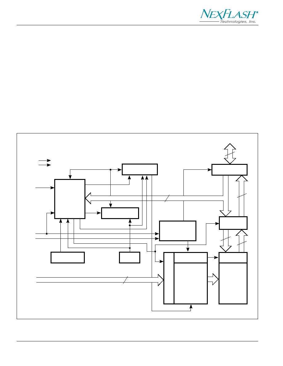
Figure 1. NX29F010 Block Diagram
Executing the Erase Command Sequence invokes the
Embedded Erase Algorithm, an internal algorithm that
automatically pre-programs the array to all zeros (if it is not
already programmed) before executing the erase operation.
During erase, the device automatically times the erase
pulse widths and verifies proper cell margin during erase.
By reading the DQ7 (
Data Polling) and DQ6 (toggle) status
bits, the host system can detect whether a program or erase
operation is complete. After completion, the device is ready
to read array data or accept another command.
The sector erase architecture is designed to allow memory
sectors to be erased and reprogrammed without affecting
the data contents of other sectors. The device is erased
before it is shipped to customers.
The hardware data protection includes a low Vcc detector
that automatically inhibits write operations during power
transitions. The hardware sector protection feature will
disable both program and erase operations in any combina-
tion of the sectors of memory, and is implemented using
standard EPROM programming algorithm.
The device electrically erases all bits within a sector
simultaneously via Fowler-Nordheim tunneling. Data are
programmed one byte at a time using the EPROM program-
ming algorithm of hot electron injection.

NX29F010
NexFlash Technologies, Inc.
3
NXPF001G-0403
04/14/03 ©
Table 1. Pin Descriptions
A0-A16
Address Inputs
DQ0-DQ7
Data Inputs/Outputs
CE
Chip Enable Input
OE
Output Enable Input
WE
Write Enable Input
Vcc
Power Supply Voltage
GND
Ground
NC
No Internal Connection
DQ1
DQ2
G
ND
DQ3
DQ4
DQ5
DQ6
A12
A15
A16
NC
VC
C
WE
NC
A14
A13
A8
A9
A11
OE
A10
CE
DQ7
A7
A6
A5
A4
A3
A2
A1
A0
DQ0
5
6
7
8
9
10
11
12
13
29
28
27
26
25
24
23
22
21
NDEX
4
3
2
1
32
31
30
14
15
16
17
18
19
20
1
2
3
4
5
6
7
8
9
10
11
12
13
14
15
16
32
31
30
29
28
27
26
25
24
23
22
21
20
19
18
17
A11
A9
A8
A13
A14
NC
WE
VCC
NC
A16
A15
A12
A7
A6
A5
A4
OE
A10
CE
DQ7
DQ6
DQ5
DQ4
DQ3
GND
DQ2
DQ1
DQ0
A0
A1
A2
A3
Figure 3. NX29F010 32-pin PLCC
Figure 4. NX29F010 32-pin TSOP
Figure 2. NX29F010 32-pin Plastic DIP
1
2
3
4
5
6
7
8
9
10
11
12
13
14
15
16
32
31
30
29
28
27
26
25
24
23
22
21
20
19
18
17
NC
A16
A15
A12
A7
A6
A5
A4
A3
A2
A1
A0
DQ0
DQ1
DQ2
GND
VCC
WE
NC
A14
A13
A8
A9
A11
OE
A10
CE
DQ7
DQ6
DQ5
DQ4
DQ3
PIN CONFIGURATIONS

NX29F010
4
NexFlash Technologies, Inc.
NXPF001G-0403
04/14/03 ©
BUS OPERATIONS
Table 2. Device Bus Operations
(1, 2)
Operation
CE
CE
CE
CE
CE
OE
OE
OE
OE
OE
WE
WE
WE
WE
WE
Address (A16-A0)
DQ0-DQ7
Read
L
L
H
A
IN
Data Out
Write
L
H
L
A
IN
Data In
Standby
V
CC
± 0.5V
X
X
X
High-Z
Output Disable
L
H
H
X
High-Z
Notes:
1. L = V
IL
, H = V
IH
, X = Don't care, AIN = Address In.
2. The sector protect and sector unprotect functions must be implemented via programming equipment.
See the Sector Protection/Unprotection section.
Requirements for Reading Array Data
Upon device power-up, or after a hardware reset, the internal
state machine is set for reading array data. This ensures
that no spurious alteration of the memory content occurs
during the power transition. No command is necessary in
this mode to obtain array data. Standard microprocessor
read cycles that assert valid addresses on the device
address inputs produce valid data on the device data
outputs. The device remains enabled for read access until
the command register contents are altered.
The system must drive the
CE and OE pins to V
IL
to read
array data from the outputs.
CE is the power control and
selects the device.
OE is the output control that passes
array data to the output pins. During a READ operation,
WE
must remain at V
IH
.
Write Commands/Command Sequences
The system must drive
WE and CE to V
IL
, and
OE to V
IH
to
write a command or command sequence (which includes
programming data to the device and erasing sectors of
memory).
An erase operation can erase one sector, multiple sectors,
or the entire device. The Sector Address Table (see Table 3)
indicate the address space that each sector occupies. A
"sector address" consists of the address bits required to
uniquely select a sector. See the "Command Definitions"
section for details on erasing a sector or the entire chip.
Table 3. Sector Addresses Table
Sector
A16
A15
A14
Address Range
Sector A0
0
0
0
00000H-03FFFH
Sector A1
0
0
1
04000H-07FFFH
Sector A2
0
1
0
08000H-0BFFFH
Sector A3
0
1
1
0C000H-0FFFFH
Sector A4
1
0
0
10000H-13FFFH
Sector A5
1
0
1
14000H-17FFFH
Sector A6
1
1
0
18000H-1BFFFH
Sector A7
1
1
1
1C000H-1FFFFH
After the system writes the auto-select command
sequence, the device enters the auto-select mode. The
system can then read auto-select codes from the internal
register (which is separate from the memory array) on
DQ7-DQ0. Standard read cycle timings apply in this mode.
Refer to the "Auto-select Mode and Auto-select Command
Sequence" sections for more information.
Program and Erase Operation Status
By reading the status bits on DQ7-DQ0, the system may
check the status of the operation during an erase or program
operation.

NX29F010
NexFlash Technologies, Inc.
5
NXPF001G-0403
04/14/03 ©
Table 4. Auto-select Codes (High Voltage Method)
Description
CE
CE
CE
CE
CE
OE
OE
OE
OE
OE
WE
WE
WE
WE
WE
A16-A14
A13-A10
A9
A8-A2
A1
A0
DQ7-DQ0
Manufacturer
L
L
H
X
X
V
ID
X
L
L
01 (Hex)
Equivalent ID
Device
L
L
H
X
X
V
ID
X
L
H
20 (Hex)
Equivalent ID
Sector Protection
L
L
H
SA
X
V
ID
X
H
L
01H
Verification
(protected)
00H
(unprotected)
Note:
1. L = V
IL
, H = V
IH
, V
ID
= 11.5
TO
12.5V , SA = A
DDRESS
S
ECTOR
, X = Don't care.
Standby Mode
In the Standby Mode, current consumption is greatly
reduced, and the outputs are placed in the high impedance
state, independent of the
OE input. The system can place
the device in the standby mode when it is not reading or
writing to the device.
The device enters the CMOS standby mode when the
CE
pin is held at V
CC
± 0.5V. The device enters the TTL standby
mode when
CE is held at V
IH
. The device requires the
standard access time (
t
CE
) before it is ready to read data.
If the device is deselected during erasure or programming,
the device draws active current until the operation is
completed.
Output Disable Mode
When the
OE = V
IH
, the output from the device is disabled
and the output pins are placed in the high-impedance state.
Auto-select Mode
The auto-select mode provides access to the manufacturer
and device equivalent codes, as well as sector protection
verification codes, via the DQ7-DQ0 pins. This mode is
primarily intended for programming equipment to automatically
match a device to be programmed with its corresponding
programming algorithm. However, the auto-select codes
can also be accessed in-system through the command
register.
When using programming equipment, the auto-select mode
requires V
ID
(11.5V to 12.5V) on address pin A9. Address
pins A1 and A0 must be as shown in Auto-select Codes
(High Voltage Method), Table 4. In addition, when verifying
sector protection, the sector address must appear on the
appropriate highest order address bits. Refer to the corre-
sponding Sector Address Table (Table 3). The Command
Definitions table shows the remaining address bits that are
don't care. When all necessary bits have been set as
required, the programming equipment may then read the
corresponding identifier code on DQ7-DQ0.
To access the auto-select codes in-system, the host
system can issue the auto-select command via the
command register, as shown in the Command Definitions
table. This method does not require V
ID
. See "Command
Definitions" for details on using the auto-select mode.
Sector Protection/Unprotection
The hardware sector protection feature disables both pro-
gram and erase operations in any sector. The hardware
sector unprotection feature re-enables both program and
erase operations in previously protected sectors.
Sector protection/unprotection procedure requires a high
voltage (V
ID
) on address pin A9 and the control pins. Details
on this method are provided in a supplement. Contact an
NexFlash representative to obtain a copy of the appropriate
document.
The device is shipped with all sectors unprotected. NexFlash
offers the option of programming and protecting sectors at
its factory prior to shipping the device. Contact a NexFlash
representative for details.
It is possible to determine whether a sector is protected or
unprotected. See "Auto-select Mode" for details.