 | –≠–ª–µ–∫—Ç—Ä–æ–Ω–Ω—ã–π –∫–æ–º–ø–æ–Ω–µ–Ω—Ç: W24129AJ | –°–∫–∞—á–∞—Ç—å:  PDF PDF  ZIP ZIP |
Document Outline
- Main Menu
- Memory Products
- Search
- Web

W24129A
16K
◊
8 HIGH-SPEED CMOS STATIC RAM
Publication Release Date: July 1995
- 1 -
Revision A2
GENERAL DESCRIPTION
The W24129A is a high-speed, low-power CMOS static RAM organized as 16384
◊
8 bits that
operates on a single 5-volt power supply. This device is manufactured using Winbond's high
performance CMOS technology.
FEATURES
∑
High-speed access time: 12/15 nS (max.)
∑
Low-power consumption:
-
Active: 400 mW (typ.)
∑
Single
+
5V power supply
∑
Fully static operation
∑
All inputs and outputs directly TTL compatible
∑
Three-state outputs
∑
Available packages: 28-pin 300 mil SOJ and
skinny DIP
PIN CONFIGURATION
A8
A9
1
2
3
4
5
24
25
26
27
28
NC
A7
A6
A5
A12
A4
A3
A2
A1
6
7
8
9
20
21
22
23
A11
A10
I/O8
I/O7
I/O6
I/O5
10
11
12
13
16
17
18
19
A0
I/O2
I/O3
I/O1
14
15
I/O4
A13
CS
OE
WE
V
DD
V
SS
BLOCK DIAGRAM
A0
.
.
CS
A13
WE
I/O1
I/O8
OE
ARRAY
V
DD
V
SS
.
.
DATA I/O
DECODER
CONTROL
CORE
ARRAY
PIN DESCRIPTION
SYMBOL
DESCRIPTION
A0
-
A13
Address Inputs
I/O1
-
I/O8
Data Inputs/Outputs
CS
Chip Select Input
WE
Write Enable Input
OE
Output Enable Input
V
DD
Power Supply
V
SS
Ground

W24129A
- 2 -
DC CHARACTERISTICS
Absolute Maximum Ratings
PARAMETER
RATING
UNIT
Supply Voltage to V
SS
Potential
-0.5 to +7.0
V
Input/Output to V
SS
Potential
-0.5 to V
DD
+0.5
V
Allowable Power Dissipation
1.0
W
Storage Temperature
-65 to +150
∞
C
Operating Temperature
0 to +70
∞
C
Note: Exposure to conditions beyond those listed under Absolute Maximum Ratings may adversely affect the life and reliability of the
device.
TRUTH TABLE
CS
OE
WE
MODE
I/O1-I/O8
V
DD
CURRENT
H
X
X
Not Selected
High Z
I
SB
,I
SB1
L
H
H
Output Disable
High Z
I
DD
L
L
H
Read
Data Out
I
DD
L
X
L
Write
Data In
I
DD
OPERATING CHARACTERISTICS
(V
DD
= 5V
±
5%, V
SS
= 0V, T
A
= 0 to 70
∞
C)
PARAMETER
SYM.
TEST CONDITIONS
MIN.
TYP.
MAX.
UNIT
Input Low Voltage
V
IL
-
-0.5
-
+0.8
V
Input High Voltage
V
IH
-
+2.2
-
V
DD
+0.5
V
Input Leakage Current
I
LI
V
IN
= V
SS
to V
DD
-10
-
+10
µ
A
Output Leakage
Current
I
LO
V
I/O
= V
SS
to V
DD,
CS = V
IH
or OE = V
IH
or WE = V
IL
-10
-
+10
µ
A
Output Low Voltage
V
OL
I
OL
= +8.0 mA
-
-
0.4
V
Output High Voltage
V
OH
I
OH
= -4.0 mA
2.4
-
-
V
Operating Power
I
DD
CS = V
IL,
I/O = 0 mA
12
-
-
160
mA
Supply Current
Cycle = MIN
15
-
-
150
mA
Standby Power
Supply Current
I
SB
CS = V
IH
Cycle = MIN, Duty = 100%
-
-
30
mA
I
SB1
CS
V
DD
-0.2V
-
-
5
mA
Note: Typical characteristics are at V
DD
= 5V, T
A
= 25
∞
C.
W24129A
Publication Release Date: July 1995
- 3 -
Revision A2
CAPACITANCE
(V
DD
= 5V, T
A
= 25
∞
C, f = 1 MHz)
PARAMETER
SYM.
CONDITIONS
MAX.
UNIT
Input Capacitance
C
IN
V
IN
= 0V
8
pF
Input/Output Capacitance
C
I/O
V
OUT
= 0V
10
pF
Note: These parameters are sampled but not 100% tested.
AC TEST CONDITIONS
PARAMETER
CONDITIONS
Input Pulse Levels
0V to 3V
Input Rise and Fall Times
5 nS
Input and Output Timing Reference Level
1.5V
Output Load
C
L
= 30 pF, I
OH
/I
OL
= -4 mA/8 mA
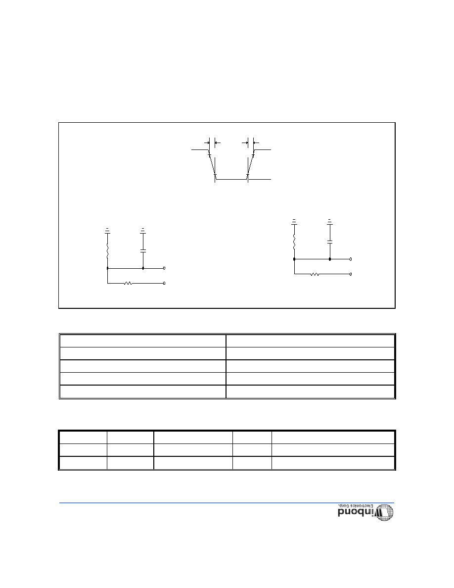
AC TEST LOADS AND WAVEFORM
90%
90%
5 nS
10%
5 nS
10%
R1 480 ohm
5V
OUTPUT
R2
255 ohm
5 pF
R2
255 ohm
R1 480 ohm
5V
OUTPUT
30 pF
Including
Jig and
Scope
3.0V
0V
Including
Jig and
Scope
)
(For T
CLZ
,
,
,
,
,
T
OLZ
T
CHZ
T
OHZ
T
WHZ
T
OW
W24129A
- 4 -
AC CHARACTERISTICS
(V
DD
= 5V
±
5%, V
SS
= 0V, T
A
= 0 to 70
∞
C)
Read Cycle
PARAMETER
SYM.
W24129A-12
W24129A-15
UNIT
MIN.
MAX.
MIN.
MAX.
Read Cycle Time
T
RC
12
-
15
-
nS
Address Access Time
T
AA
-
12
-
15
nS
Chip Select Access Time
T
ACS
-
12
-
15
nS
Output Enable to Output Valid
T
AOE
-
6
-
7
nS
Chip Selection to Output in Low Z
T
CLZ
3
-
3
-
nS
Output Enable to Output in Low Z
T
OLZ
0
-
0
-
nS
Chip Deselection to Output in High Z
T
CHZ
-
6
-
7
nS
Output Disable to Output in High Z
T
OHZ
-
6
-
7
nS
Output Hold from Address Change
T
OH
3
-
3
-
nS
These parameters are sampled but not 100% tested.
Write Cycle
PARAMETER
SYM.
W24129A-12
W24129A-15
UNIT
MIN.
MAX.
MIN.
MAX.
Write Cycle Time
T
WC
12
-
15
-
nS
Chip Selection to End of Write
T
CW
10
-
13
-
nS
Address Valid to End of Write
T
AW
10
-
13
-
nS
Address Setup Time
T
AS
0
-
0
-
nS
Write Pulse Width
T
WP
10
-
10
-
nS
Write Recovery Time
CS, WE
T
WR
0
-
0
-
nS
Data Valid to End of Write
T
DW
7
-
9
-
nS
Data Hold from End of Write
T
DH
0
-
0
-
nS
Write to Output in High Z
T
WHZ
-
7
-
8
nS
Output Disable to Output in High Z
T
OHZ
-
7
-
8
nS
Output Active from End of Write
T
OW
0
-
0
-
nS
These parameters are sampled but not 100% tested.
W24129A
Publication Release Date: July 1995
- 5 -
Revision A2
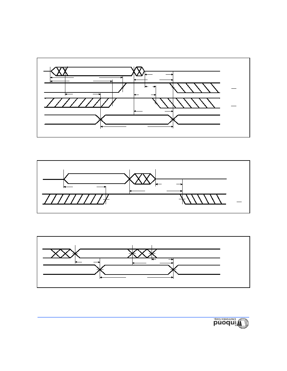
TIMING WAVEFORMS
Read Cycle 1
(Address Controlled)
Address
T
RC
T
AA
T
OH
T
OH
D
OUT
Read Cycle 2
(Chip Select Controlled)
CS
D
OUT
T
CLZ
T
ACS
CHZ
T
Read Cycle 3
(Output Enable Controlled)
Address
T
RC
CS
D
OUT
T
AA
OE
T
AOE
T
OLZ
T
OH
CLZ
T
CHZ
T
T
ACS
T
OHZ
W24129A
- 6 -
Timing Waveforms, continued
Write Cycle 1
(OE Clock)
Address
OE
CS
WE
D
OUT
D
IN
T
WC
T
WR
T
CW
T
WP
T
AS
T
OHZ
(1,4)
T
DW
T
DH
T
AW
Write Cycle 2
(OE = V
IL
Fixed)
Address
CS
WE
D
OUT
D
IN
T
WC
T
CW
T
AS
T
DH
T
WR
T
WP
T
WHZ
DW
T
(2)
(3)
T
OW
T
OH
AW
T
(1,4)
Notes:
1. During this period, I/O pins are in the output state, so input signals of opposite phase to the outputs should not be applied.
2. The data output from D
OUT
are the same as the data written to D
IN
during the write cycle.
3. D
OUT
provides the read data for the next address.
4. Transition is measured
±
500 mV from steady state with C
L
= 5 pF. This parameter is guaranteed but not 100% tested.
W24129A
Publication Release Date: July 1995
- 7 -
Revision A2
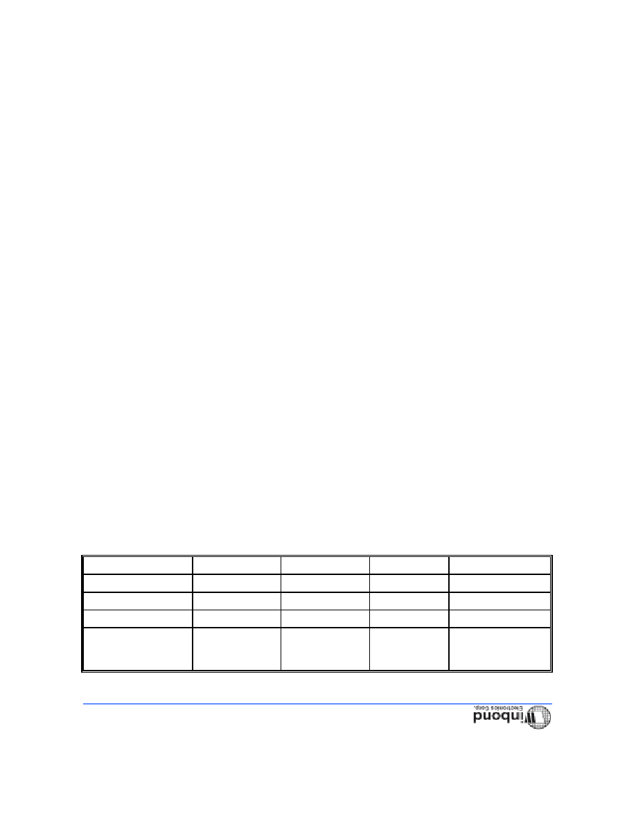
ORDERING INFORMATION
PART NO.
ACCESS
TIME (nS)
OPERATING
CURRENT
MAX. (mA)
STANDBY
CURRENT
MAX. (mA)
PACKAGE
W24129AK-12
12
160
5
300 mil skinny DIP
W24129AK-15
15
150
5
300 mil skinny DIP
W24129AJ-12
12
160
5
300 mil SOJ
W24129AJ-15
15
150
5
300 mil SOJ
Notes:
1. Winbond reserves the right to make changes to its products without prior notice.
2. Purchasers are responsible for performing appropriate quality assurance testing on products intended for use in
applications where personal injury might occur as a consequence of product failure.
W24129A
- 8 -
PACKAGE DIMENSIONS
28-pin P-DIP Skinny
1. Dimension D Max. & S include mold flash or
tie bar burrs.
2. Dimension E1 does not include interlead flash.
3. Dimension D & E1 include mold mismatch and
are determined at the mold parting line.
6. General appearance spec. should be based on
final visual inspection spec.
1.63
1.47
0.064
0.058
Notes:
Symbol
Min.
Nom.
Max.
Max.
Nom.
Min.
Dimension in Inches
Dimension in mm
A
B
c
D
e
A
L
S
A
A
1
2
E
0.060
1.52
0.175
4.45
0.010
0.125
0.016
0.130
0.018
0.135
0.022
3.18
0.41
0.25
3.30
0.46
3.43
0.56
0.008
0.120
0.370
0.010
0.130
0.014
0.140
0.20
3.05
0.25
3.30
0.36
3.56
0.293
0.288
0.283
7.44
7.32
7.19
9.40
7.87
7.62
8.13
0.310
0.300
0.320
2.29
2.54
2.79
0.090
0.100
0.110
B
1
1
e
E
1
a
1.388
1.400
35.26
35.56
0
15
0.055
1.40
0.350
0.330
8.38
8.89
15
0
4. Dimension B1 does not include dambar
protrusion/intrusion.
5. Controlling dimension: Inches.
e
A
A
a
c
E
Base Plane
Mounting Plane
1
A
1
e
L
A
S
1
E
D
1
B
B
28
15
1
14
2
28-pin Small Outline J Band
1
y
1
e
s
1
b
b
c
L
e
Seating Plane
1
2
A
A
A
D
E
H
E
14
15
28
£c
0.36
0.20
0.014
0.008
Symbol
Min. Nom.
Max.
Max.
Nom.
Min.
Dimension in Inches
Dimension in mm
A
b
c
D
e
H
E
L
y
A
A
S
1
1
2
E
0.010
0.25
0.140
3.56
0.027
0.095
0.016
0.100
0.018
0.105
0.022
2.41
0.41
0.69
2.54
0.46
2.67
0.56
0.077
0.004
0
10
0.710
0.087
0.730
0.097
1.96
18.03
2.21
18.54
2.46
0.285
0.265
0.245
7.24
6.73
6.22
0
0.10
7.75
7.62
7.49
0.305
0.300
0.295
8.31
8.56
8.81
0.327
0.337
0.347
1. Dimension D Max. & S include mold flash
or tie bar burrs.
2. Dimension b does not include dambar
protrusion/intrusion.
4. Controlling dimension: Inches.
5. General appearance spec. should be based
on final visual inspection spec.
Notes:
3. Dimension D & E include mold mismatch
and are determined at the mold parting line.
e
b
1
0.81
0.71
0.66
0.032
0.028
0.026
0.044
0.050
0.056
1.12
1.27
1.42
0.045
1.14
10

W24129A
Publication Release Date: July 1995
- 9 -
Revision A2
Headquarters
No. 4, Creation Rd. III,
Hsinchu, Taiwan
TEL: 886-3-5770066
FAX: 886-3-5792647
http://www.winbond.com.tw/
Voice & Fax-on-demand: 886-2-7197006
Taipei Office
11F, No. 115, Sec. 3, Min-Sheng East Rd.,
Taipei, Taiwan
TEL: 886-2-7190505
Winbond Electronics (H.K.) Ltd.
Rm. 803, World Trade Square, Tower II,
Kowloon, Hong Kong
TEL: 852-27513100
FAX: 852-27552064
Winbond Electronics North America Corp.
Winbond Memory Lab.
Winbond Microelectronics Corp.
Winbond Systems Lab.
CA 95134, U.S.A.
TEL: 1-408-9436666
FAX: 1-408-9436668
Note: All data and specifications are subject to change without notice.