 | –≠–ª–µ–∫—Ç—Ä–æ–Ω–Ω—ã–π –∫–æ–º–ø–æ–Ω–µ–Ω—Ç: W53300 | –°–∫–∞—á–∞—Ç—å:  PDF PDF  ZIP ZIP |
Document Outline
- Main Menu
- Speech Products
- Search
- Web

W53300/W53320
16" Voice/Melody/LCD Controller
(ViewTalk
TM
Series)
Publication Release Date: March 1999
- 1 - Revision A2
GENERAL DESCRIPTION
The W53300/W53320 are a high-performance 4-bit microcontroller (
µ
C) with built-in speech, melody
and 16*48/32*48 LCD driver which includes internal pump circuit. The 4-bit uc core contains dual
clock source, 4-bit ALU, two 8-bit timers, one divider, 20 pin input or output, 7 interrupt sources and
8-level subroutine nesting for interrupt applications. Speech unit can be implemented with Winbond
16-sec Power Speech using ADPCM algorithm. Melody unit provides dual tone output and can store
up to 1k notes. Power reduction mode is also built in to minimize power dissipation. It is ideal for
games, educational toys, remote controllers, watches, clocks and other application products which
incorporate both LCD display and melody.
FEATURES
∑
Operating voltage: 2.4 volt ~ 5.5 volt
∑
Dual clock operating system
-
RC/Crystal (400 KHz to 4 MHz) for main clock
-
32.768 KHz crystal oscillation circuit for sub-oscillator
∑
Memory
-
Program ROM: 16K
◊
20
-
Data RAM: 512
◊
4 bit (W53320), 704
◊
4 bit(W53300)
-
LCD RAM: 384
◊
4 bit (W53320), 192
◊
4 bit (W53300)
∑
20 input/output pins
-
Ports for input only: 2 ports/8 pins
-
Input/output ports: 2 ports/8 pins
-
Port for output only: 1 port /4 pins
∑
Power-down mode
-
Hold function: no operation (except for oscillator)
∑
Seven types of interrupts
-
Five internal interrupts (Divider ,Timer 0, Timer 1, Speech, Melody)
-
Two external interrupts (Port RC, Port RD)
∑
One built-in 14-bit clock frequency divider circuit
∑
Two built-in 8-bit programmable countdown timers
-
Timer 0: one of two internal clock frequencies (FOSC/4 or FOSC/1024) can be selected
-
Timer 1: built-in auto-reload function includes internal timer, external event counter from RC.0
or TONE output function (can be used as IR carrier output if main clock is 455 kHz)
∑
Built-in 18/14-bit watchdog timer for system reset by mask code option
∑
Powerful instruction sets
∑
8-level subroutine (including interrupt) nesting

W53300/W53320
- 2 -
∑
LCD driver output
-
32 com
◊
48 seg (W53320), 16 com
◊
48 seg (W53300)
-
1/16 or 1/32 duty, 1/5 or 1/7 bias, internal pump circuit option by special register
∑
Speech function
-
Provides 384 kbits dedicated speech ROM
-
Direct driving output for speaker
-
Maximum 256 sections available
∑
Melody function
-
Provides 22 kbits dedicated melody ROM
-
Provides 6 kinds of beat, 16 kinds of tempo, and pitch range from G3# to C7
-
Tremolo, triple frequency and 3 kinds of percussion available
-
Direct driving output for speaker
-
Maximum 32 scores available
∑
Mix speech with melody available
∑
Multi-engine controller
∑
PWM output current option
∑
Chip On Board available
W53300/W53320
Publication Release Date: March 1999
- 3 - Revision A2
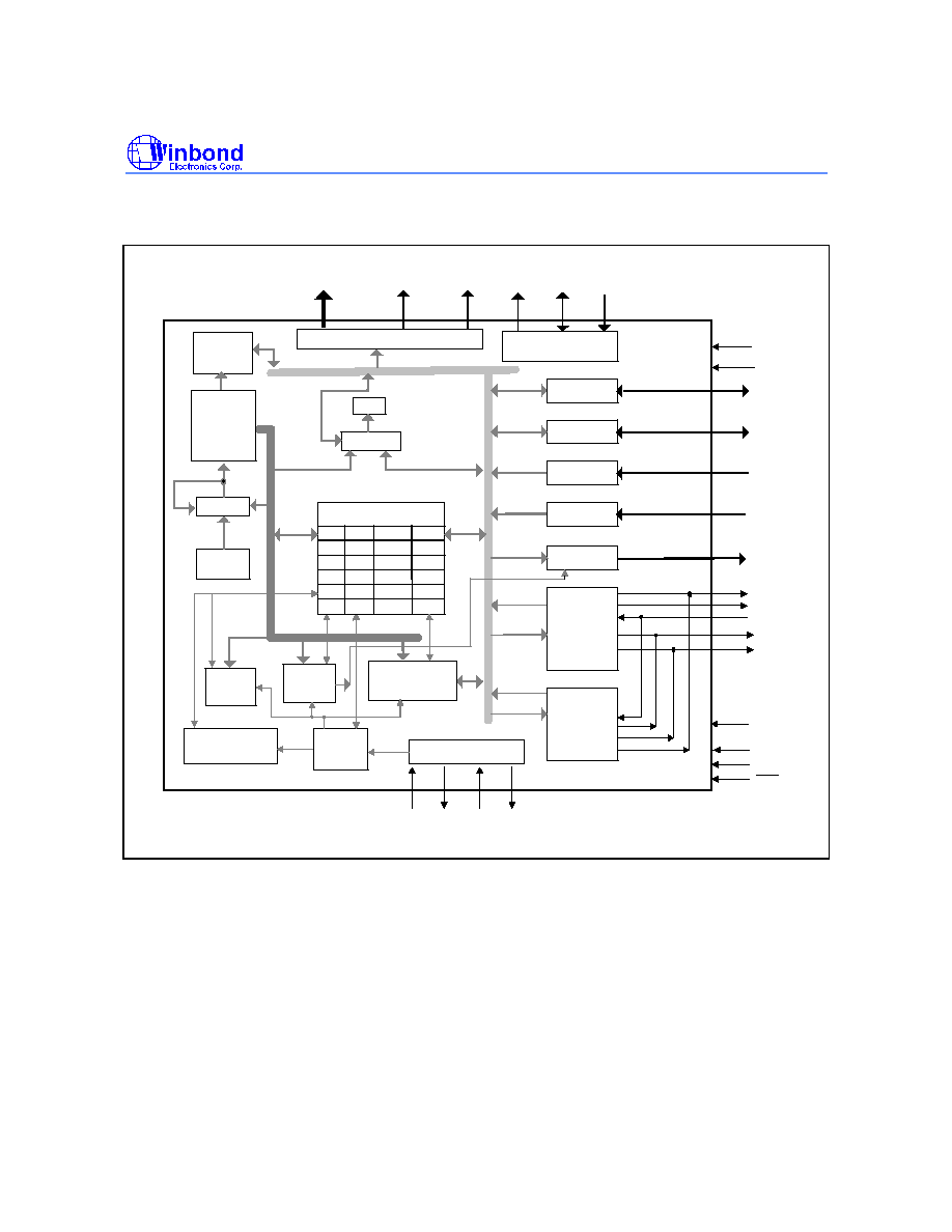
BLOCK DIAGRAM
LCD DRIVER
PC
STACK
(8 Levels)
(896*4)
Timer 0
(8 Bit)
Timing Generator
SEG0 to SEG47
V2 ~ V6
XIN
XOUT
Timer 1
(8 Bit)
Watch Dog Timer
(18/14 Bit)
VDD2
ALU
ACC
Divider
(14/10 Bit)
X32I
X32O
ROM
(16K*20)
DH1, DH2
COM0 to COM31
RAM
Interrup & Hold
Mode Release
Special Register
.
.
HCF
HEF
IEF
EVF
FLAG1
PSR0
MR1
MLDH
PEF
SPCH
FLAG0
LUP2
PM0
.
.
LUP3
LUP0 LUP1
LUC
RP0L
RP0M
RP0H
PORT RB
PORT RD
PORT RC
PORT RE
Speech
Dual Tone
Melody
(1K*22 ROM)
(384Kbit ROM)
PORT RA
VLCD PUMP CIRCUIT
MLD_play
MLD_busy
SPC_busy
SPC_busy
TONE
TEST
RA0~3
RB0~3
RD0~3
RC0~ 3
RE0 to 3
VDD
LED1
LED2
VSS1
RES
VDDP
PWM1
PWM2
ROSC
VDD3
VSS2
W53300/W53320
- 4 -
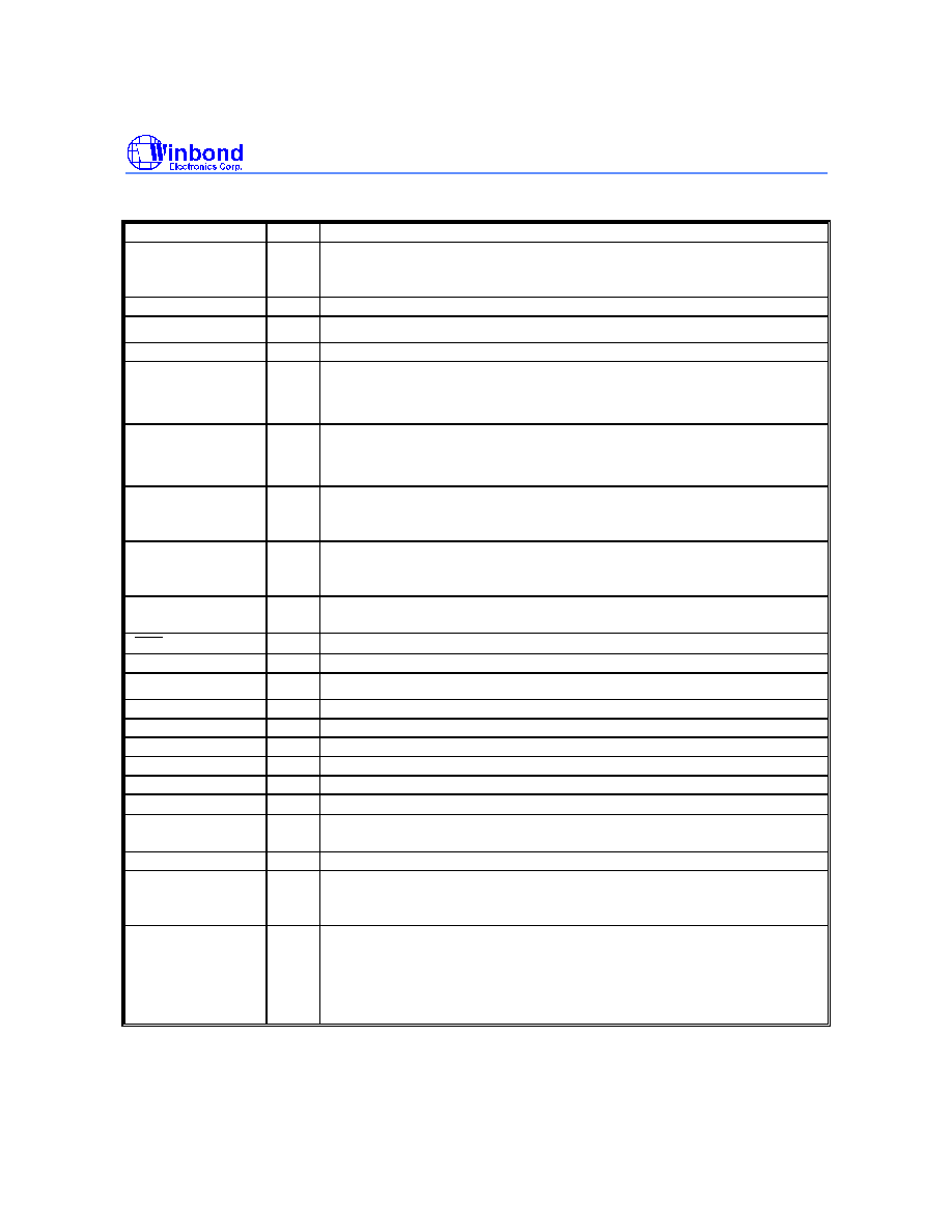
PIN DESCRIPTION
SYMBOL
I/O
FUNCTION
XIN
I
Input pin for oscillator. It can be connected to crystal, or can connect a
resistor to VDD to generate main system clock. Oscillator can be
stopped when SCR.1 is set to logic 1.
XOUT
O
Output pin for oscillator which is connected to another crystal pin.
X32I
I
32.768 KHz crystal input pin.
X32O
O
32.768 KHz crystal output pin.
RA0 ~ RA3
I/O
General Input/Output port specified by PM1 register. If output mode is
selected, PM0 register can be used to specify CMOS/NMOS driving
capability option. Initial state is input mode.
RB0 ~ RB3
I/O
General Input/Output port specified by PM2 register. If output mode is
selected, PM0 register can be used to specify CMOS/NMOS driving
capability option. Initial state is input mode.
RC0 ~ RC3
I
4-bit schmitt input with internal pull high option specified by PM0
register. RC0 can be used as clock source for Timer 1. Each pin has
an independent interrupt capability specified by PEFL special register.
RD0 ~ RD3
I
4-bit schmitt input port with internal pull high option specified by PM0
register. Each pin has an independent interrupt capability specified by
PEFH special register.
RE0~RE3/TONE
O
Output port only. RE3 may use as TONE if bit 0 of MR0 special
register is set to logic 1.
RES
I
System reset pin with internal pull-high resistor is active low.
TEST
I
Test pin. No connect for normal use.
ROSC
I
Connects resistor to VDD to generate speech or melody clock source.
VDDP
I
Power source for PWM output.
LED1
O
Synchronous LED1 output while speech play/melody is active.
LED2
O
Synchronous LED2 output only while speech play is active.
PWM1
O
Speaker direct driving output 1 while speech or melody is active.
PWM2
O
Speaker direct driving output 2 while speech or melody is active.
SEG0
-
SEG47
O
LCD segment output pins.
COM0
-
COM31
O
LCD common signal output pins. The LCD alternating frequency is
fixed at 64Hz. COM16~31 are useless for W53300.
DH1, DH2
I
Connection terminals for voltage doubler capacitor.
VDD2
O
Connects a 1uF capacitor to VSS1 to double VDD voltage output if
triple pump option is enabled. Otherwise, VDD2 connects to VDD
directly if double pump option is enabled.
VDD3
O/I
An output if internal pump circuit is enabled. It connects a 1uF
capacitor to VSS. Triple VDD voltage will be output if triple pump
option is enabled. Otherwise, double VDD voltage will be output if
double pump option is enabled.
An input if internal pump voltage is disabled.
W53300/W53320
Publication Release Date: March 1999
- 5 - Revision A2
V2 ~ V5
O
LCD COM/SEG output driving voltage. If internal shunt resistor is
disabled, external resistors need to be supplied to V2, V3, V4, V5 . A
capacitor is suggestted for stable LCD voltage level.
V6
I
External variable resistor connects between VDD3 and V6 to adjust
LCD maximun voltage level.
VDD
I
Microcontroller Positive power supply (+).
VSS1
I
Negative power supply (-).
VSS2
I
Negative power supply (-).
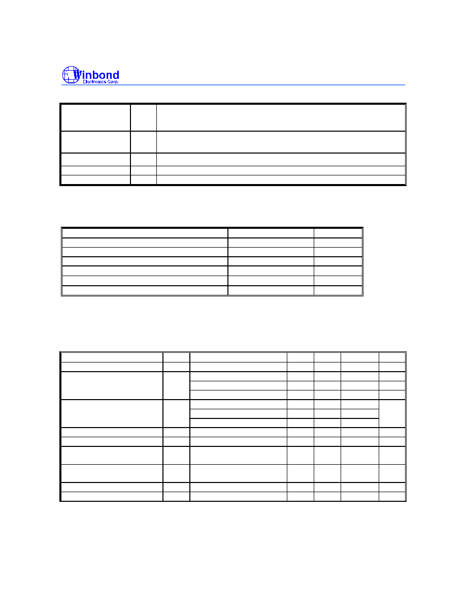
ABSOLUTE MAXIMUM RATINGS
PARAMETER
RATING
UNIT
Supply Voltage to Ground Potential
-0.3 to +7.0
V
Applied Input/Output Voltage
-0.3 to +7.0
V
Power Dissipation
120
mW
Ambient Operating Temperature
0 to +70
∞
C
Storage Temperature
-55 to +150
∞
C
VDD3 Input Voltage
12
V
Note: Exposure to conditions beyond those listed under Absolute Maximum Ratings may adversely
affect the life and reliability of the device.
DC CHARACTERISTICS
(VDD
-
VSS = 3.0V, F
M
= 1 MHz, Fs = 32.768 KHz, TA = 25
∞
C, LCD on; unless otherwise specified)
PARAMETER
SYM. CONDITIONS
MIN.
TYP.
MAX.
UNIT
Op. Voltage
V
DD
2.4
5.5
V
Op. Current
I
OP1
Dual clock with crystal
-
250
300
uA
(No Load)
Dual clock with RC type
250
300
uA
Single Clock
60
100
uA
Halt Mode Current
Iop2
Dual clock with crystal
120
150
uA
(No Load, LCD OFF)
Dual clock with RC type
120
150
uA
Single clock
6
10
uA
Input Low Voltage
V
IL
-
VSS
-
0.3*VDD
V
Input High Voltage
V
IH
-
0.7
-
1
VDD
Port RA, RB Output Low
Voltage
V
ABL
IOL = 2.0 mA
-
-
0.4
V
Port RA, RB Output High
Voltage
V
ABH
IOH = -2.0 mA
2.4
-
-
V
Port RE Sink Current
I
EL
VOL = 0.4V
2
-
-
mA
Port RE Source Current
I
EH
VOH = 2.4V
-2
-
-
mA