
W742E/C816
4-BIT MICROCONTROLLER
Publication Release Date: December 17, 2001
- 1 - Revision A1
Table of Contents-
1.
GENERAL DESCRIPTION ......................................................................................................................3
2.
FEATURES .............................................................................................................................................3
3.
PIN CONFIGURATION............................................................................................................................5
4.
PIN DESCRIPTION .................................................................................................................................6
5.
FUNCTIONAL DESCRIPTION ................................................................................................................7
5.1
Program Counter (PC)..............................................................................................................7
5.2
Stack Register (STACK)...........................................................................................................8
5.3
Program Memory (ROM) ..........................................................................................................8
5.3.1
ROM Page Register (ROMPR) ...........................................................................................9
5.3.2
ROM Addressing Mode ....................................................................................................10
5.4
Data Memory (RAM)...............................................................................................................11
5.4.1
Architecture ......................................................................................................................11
5.4.2
RAM Page Register (PAGE).............................................................................................12
5.4.3
WR Page Register (WRP)................................................................................................12
5.4.4
Data Bank Register (DBKRH, DBKRL).............................................................................13
5.4.5
RAM Addressing Mode .....................................................................................................14
5.5
Accumulator (ACC).................................................................................................................15
5.6
Arithmetic and Logic Unit (ALU) .............................................................................................15
5.7
Main Oscillator........................................................................................................................16
5.8
Sub-oscillator..........................................................................................................................16
5.9
Dividers...................................................................................................................................16
5.10
Dual-clock Operation ..............................................................................................................17
5.11
Watchdog Timer (WDT) .........................................................................................................18
5.12
Timer/Counter.........................................................................................................................19
5.12.1
Timer 0 (TM0) .................................................................................................................19
5.12.2
Timer 1 (TM1) .................................................................................................................20
5.12.3
Mode Register 0 (MR0) ..................................................................................................21
5.12.4
Mode Register 1 (MR1) ..................................................................................................22
5.13
Interrupts ................................................................................................................................22
5.14
Stop Mode Operation .............................................................................................................24
5.14.1
Stop Mode Wake-up Enable Flag for RC and RD Port (SEF) ........................................24
5.15
Hold Mode Operation .............................................................................................................24
5.15.1
Hold Mode Release Enable Flag (HEF, HEFD)..............................................................26
5.15.2
Interrupt Enable Flag (IEF) .............................................................................................26
5.15.3
Port Enable Flag (PEF, P1EF)........................................................................................27
5.15.4
Hold Mode Release Condition Flag (HCF, HCFD) .........................................................27
5.15.5
Event Flag (EVF, EVFD).................................................................................................28

W742E/C816
- 2 -
5.16
Reset Function .......................................................................................................................29
5.17
Input/Output Ports RA, RB & P0.............................................................................................29
5.17.1
Port Mode 0 Register (PM0) ...........................................................................................30
5.17.2
Port Mode 1 Register (PM1) ...........................................................................................31
5.17.3
Port Mode 2 Register (PM2) ...........................................................................................31
5.17.4
Port Mode 6 Register (PM6) ...........................................................................................32
5.18
Serial I/O interface..................................................................................................................32
5.19
Input Ports RC ........................................................................................................................35
5.19.1
Port Status Register 0 (PSR0)........................................................................................36
5.20
Input Ports RD ........................................................................................................................36
5.20.1
Port Status Register 1 (PSR1)........................................................................................37
5.21
Output Port RE & RF ..............................................................................................................38
5.22
Input Port P1...........................................................................................................................38
5.23
DTMF Output Pin (DTMF) ......................................................................................................38
5.23.1
DTMF Register ...............................................................................................................39
5.23.2
Dual Tone Control Register (DTCR) ...............................................................................39
5.24
FSK Output.............................................................................................................................40
5.24.1
FSK Transmit Control Register (FSKC) ..........................................................................41
5.24.2
FSK Transmit Data Buffer (FSKB) ..................................................................................41
5.25
MFP Output Pin (MFP) ...........................................................................................................41
5.26
LCD Controller/Driver .............................................................................................................43
5.26.1
LCD RAM Addressing Method........................................................................................44
5.26.2
LCD Voltage and Contrast Adjusting ..............................................................................44
5.26.3
SEG32
-
SEG39 Using as DC Output (NMOS Open Drain Type) .................................46
5.26.4
The Output Waveforms for the LCD Driving Mode .........................................................46
6.
ABSOLUTE MAXIMUM RATINGS ........................................................................................................47
7.
DC CHARACTERISTICS.......................................................................................................................47
8.
AC CHARACTERISTICS.......................................................................................................................48
9.
INSTRUCTION SET TABLE..................................................................................................................49
10.
PACKAGE DIMENSIONS .....................................................................................................................57

W742E/C816
Publication Release Date: December 17, 2001
- 3 - Revision A1
1. GENERAL DESCRIPTION
The W742E/C816 [W742E 816 is EEPROM type, W742C816 is mask type] is a high-performance 4-
bit microcontroller (
�
C) that built in 640-dot LCD driver. The device contains a 4-bit ALU, two 8-bit
timers, two dividers in dual-clock operation, a 40
�
16 LCD driver, ten 4-bit I/O ports (including 2 output
port for LED driving), multiple frequency output, one
channel DTMF generator and FSK modulator of
CCITT V.23 or Bellcore 202. There are also eleven interrupt sources and 16-level stack buffer. The
W742E/C816 operates on very low current and has three power reduction modes, hold mode, stop
mode and slow mode, which help to minimize power dissipation.
2. FEATURES
�
Operating voltage
-
2.4V - 6.0V for mask type
-
2.4V - 4.8V for EEPROM type
�
Dual-clock operation
�
Main oscillator
-
3.58 MHz or 400 KHz can be selected by code option
-
Crystal or RC oscillator can be selected by code option
�
Sub-oscillator
-
Connect to 32.768 KHz crystal only
�
Memory
-
32768(32K) x 16 bit program ROM (including 64K x 4 bit look-up table)
-
5120(5K) x 4 bit data RAM (including 16 nibbles x 16 pages working registers)
-
40 x 16 LCD data RAM
�
40 input/output pins
-
Port for input only: 3 ports/12 pins
-
Input/output ports: 3 ports/12 pins
-
High sink current output port for LED driving: 2 port /8 pins
-
DC output port: 2 ports/ 8 pins (selected by code option)
�
Power-down mode
-
Hold mode: no operation (main oscillator and sub-oscillator still operate)
-
Stop mode: no operation (main oscillator and sub-oscillator are stopped)
-
Slow mode: main oscillator is stopped, system is operated by the sub-oscillator (32.768 KHz)

W742E/C816
- 4 -
�
Eleven interrupt sources
-
Four internal interrupts (Divider0, Divider1, Timer 0, Timer 1)
-
Seven external interrupts (RC.0
-
3, P1.2 ( INT0 ), Serial Port, P1.3 ( INT1 ))
�
LCD driver output
-
40 segments x 16 commons
-
1/8 or 1/16 duty (selected by code option) 1/5 bias driving mode
-
Clock source should be the sub-oscillator clock in the dual-clock operation mode
-
8 level software LCD contrast adjusting
-
LCD operating voltage source could come from V
DD
or VLCD1 pin input
�
MFP output pin
-
Output is software controlled to generate modulating or non-modulating frequency
-
Works as frequency output specified by Timer 1
-
Key tone generator
�
DTMF output pin
-
Output is one channel Dual Tone Multi-Frequency signal for dialing
�
FSK output
-
Output FSK signal of CCITT V.23 or Bellcore 202 by mask option
�
8-bit Serial I/O Interface
-
8-bit transmit/receive mode by internal or external clock source
�
Two built-in 14-bit frequency dividers
-
Divider0: the clock source is the main oscillator (F
OSC
)
-
Divider1: the clock source is the sub-oscillator (Fs)
�
Two built-in 8-bit programmable countdown timers
-
Timer 0: one of two internal clock frequencies (F
OSC
/4 or F
OSC
/1024) can be selected
-
Timer 1: with auto-reload function and one of two internal clock frequencies (F
OSC
or F
OSC
/64 or
Fs) can be selected (signal output through MFP pin)
�
Built-in 18/14-bit watchdog timer selectable for system reset, enable/disable by code option
�
16-level stack buffer
�
Packaged in 100-pin QFP
W742E/C816
Publication Release Date: December 17, 2001
- 5 - Revision A1
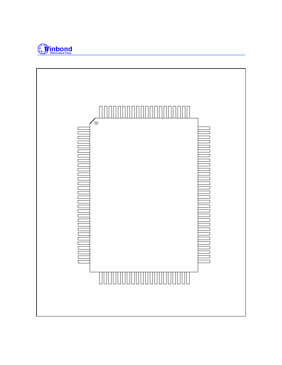
3. PIN CONFIGURATION
4
5
6
7
8
9
10
11
12
13
14
15
16
17
1
2
3
18
19
9
7
8
9
0
1
2
3
4
5
6
7
8
9
20
21
22
23
24
0
1
2
3
3
3
3
4
5
3
3
3
6
3
7
8
3
3
9
0
4
51
52
53
54
55
56
57
58
59
60
61
62
63
64
0
6
5
25
26
27
28
29
30
4
1
2
3
4
5
6
7
8
9
4
4
4
4
4
4
4
4
5
65
66
67
68
69
70
71
72
73
74
75
76
77
78
79
80
1
2
3
4
8
8
8
8
8
8
8
8
8
9
9
9
9
9
9
9
9
9
1
0
S E G 3 5
S E G 3 6
S E G 3 7
S E G 3 8
C O M 1 5
S E G 3 9
C O M 1 4
C O M 1 2
C O M 1 1
C O M 0 8
P01
P00
P11
P12
P13
C N
S E G 0 2
S E G 0 8
C P
V L C D 1
C O M 0 2
C O M 0 3
C O M 0 4
C O M 0 5
C O M 0 6
C O M 0 7
S E G 0 0
S
E
G
1
5
S
E
G
1
4
S
E
G
1
3
S
E
G
1
2
X
I
N
1
X
O
U
T
1
R
C
0
R
C
1
R
C
3
R
D
0
C O M 1 3
R
C
2
S
E
G
1
8
S
E
G
1
7
S
E
G
3
0
C O M 1 0
C O M 0 9
C O M 0 0
S
E
G
1
6
R
D
2
M F P
R
D
1
R A 0
S E G 0 7
S
E
G
1
1
C O M 0 1
S E G 3 2
S E G 3 1
S E G 3 3
S E G 3 4
R A 2
R A 3
R B 0
R B 1
R B 2
R B 3
X O U T 2
XIN2
V S S
R
D
3
R
E
0
R
E
1
R
E
2
R
E
3
R
F
0
R
F
1
R
F
2
R
F
3
/
R
E
S
E
T
V
D
D
P02
P03
P10
S E G 0 1
S E G 0 3
S E G 0 4
S E G 0 5
S E G 0 6
S E G 0 9
S E G 1 0
S
E
G
1
9
S
E
G
2
0
S
E
G
2
1
S
E
G
2
2
S
E
G
2
3
S
E
G
2
4
S
E
G
2
7
S
E
G
2
8
S
E
G
2
9
S
E
G
2
5
S
E
G
2
6
R A 1
DTMF/FSK
(K0.0)
(K0.1)
(K0.2)
(K0.3)
(K1.0)
(K1.1)
(K1.2)
(K1.3)
[Data_IO]
[Vpp]
[mode]
W742E/C816
100-pin QFP