 | –≠–ª–µ–∫—Ç—Ä–æ–Ω–Ω—ã–π –∫–æ–º–ø–æ–Ω–µ–Ω—Ç: W77IC32P | –°–∫–∞—á–∞—Ç—å:  PDF PDF  ZIP ZIP |
Document Outline
- Main Menu
- 8-bit µC Products
- Search
- Web

Preliminary W77IC32
8 BIT MICROCONTROLLER
Publication Release Date: March 2000
- 1 - Revision A0
GENERAL DESCRIPTION
The W77IC32 is a fast 8051 compatible microcontroller with a redesigned processor core without
wasted clock and memory cycles. As a result, it executes every 8051 instruction faster than the
original 8051 for the same crystal speed. Typically, the instruction executing time of W77IC32 is 1.5
to 3 times faster then that of traditional 8051, depending on the type of instruction. In general, the
overall performance is about 2.5 times better than the original for the same crystal speed. Giving the
same throughput with lower clock speed, power consumption has been improved. Consequently, the
W77IC32 is a fully static CMOS design; it can also be operated at a lower crystal clock. W77IC32
support on-chip 1KB SRAM without external memory component and glue logic, saving more I/O pins
for users application usage if they use on-chip SRAM instead of external SRAM.
FEATURES
∑
8-bit CMOS microcontroller
∑
High speed architecture of 4 clocks/machine cycle
∑
Pin compatible with standard 80C52
∑
Instruction-set compatible with MCS-51
∑
Four 8-bit I/O Ports
∑
One extra 4-bit I/O port and Wait State control signal (available on 44-pin PLCC/QFP package)
∑
Three 16-bit Timers
∑
12 interrupt sources with two levels of priority
∑
On-chip oscillator and clock circuitry
∑
Two enhanced full duplex serial ports
∑
256 bytes scratch-pad RAM
∑
1KB on-chip SRAM for MOVX instruction
∑
Programmable Watchdog Timer
∑
Dual 16-bit Data Pointers
∑
Software programmable access cycle to external RAM/peripherals
∑
Packages:
-
DIP 40: W77IC32-25
-
PLCC 44: W77IC32P-25
Preliminary W77IC32
- 2 -
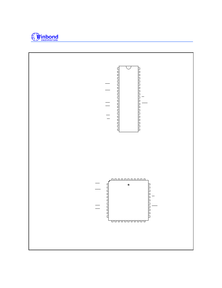
PIN CONFIGURATIONS
VDD
1
2
3
4
5
6
7
8
9
10
11
12
13
14
15
16
17
18
19
20
39
40
34
35
36
37
38
30
31
32
33
26
27
28
29
21
22
23
24
25
P0.0, AD0
P0.1, AD1
P0.2, AD2
P0.3, AD3
P0.4, AD4
P0.5, AD5
P0.6, AD6
P0.7, AD7
EA
ALE
PSEN
P2.5, A13
P2.6, A14
P2.7, A15
P2.0, A8
P2.1, A9
P2.2, A10
P2.3, A11
P2.4, A12
T2, P1.0
40-Pin DIP (W77IC32)
RXD1, P1.2
TXD1, P1.3
INT2, P1.4
INT3, P1.5
INT4, P1.6
RXD, P3.0
TXD, P3.1
INT5, P1.7
RST
INT0, P3.2
INT1, P3.3
T0, P3.4
T1, P3.5
WR, P3.6
RD, P3.7
XTAL1
XTAL2
VSS
T2EX, P1.1
44-Pin PLCC (W77IC32P)
40
2 1 44 43 42 41
6 5 4 3
39
38
37
36
35
34
33
32
31
30
29
P0.4, AD4
P0.5, AD5
P0.6, AD6
P0.7, AD7
EA
P4.1
ALE
PSEN
P2.7, A15
P2.6, A14
P2.5, A13
28
27
26
25
24
23
22
21
20
19
18
17
10
9
8
7
14
13
12
11
16
15
INT3, P1.5
INT4, P1.6
INT5, P1.7
RST
RXD, P3.0
P4.3
TXD, P3.1
INT0, P3.2
INT1, P3.3
T0, P3.4
T1, P3.5
X
T
A
L
1
V
S
S
P
2
.
4
,
A
1
2
P
2
.
3
,
A
1
1
P
2
.
2
,
A
1
0
P
2
.
1
,
A
9
P
2
.
0
,
A
8
X
T
A
L
2
P
3
.
7
,
/
R
D
P
3
.
6
,
/
W
R
A
D
3
,
P
0
.
3
T
2
,
P
1
.
0
P
1
.
2
V
D
D
A
D
2
,
P
0
.
2
A
D
1
,
P
0
.
1
A
D
0
,
P
0
.
0
T
2
E
X
,
P
1
.
1
P
1
.
3
P
1
.
4
,
X
D
1
R
,
X
D
1
T
,
N
T
2
I
P
4
.
2
P
4
.
0
,
/
W
A
I
T
Preliminary W77IC32
Publication Release Date: March 2000
- 3 - Revision A0
PIN DESCRIPTION
SYMBOL TYPE
DESCRIPTIONS
EA
I
EXTERNAL ACCESS ENABLE: It should be kept low.
PSEN
O PROGRAM STORE ENABLE:
PSEN
enables the external ROM data onto the
Port 0 address/data bus during fetch and MOVC operations.
ALE
O
ADDRESS LATCH ENABLE: ALE is used to enable the address latch that
separates the address from the data on Port 0.
RST
I
RESET: A high on this pin for two machine cycles while the oscillator is running
resets the device.
XTAL1
I
CRYSTAL1: This is the crystal oscillator input. This pin may be driven by an
external clock.
XTAL2
O
CRYSTAL2: This is the crystal oscillator output. It is the inversion of XTAL1.
V
SS
I
GROUND: Ground potential
V
DD
I
POWER SUPPLY: Supply voltage for operation.
P0.0
-
P0.7
I/O
PORT 0: Port 0 is an open-drain bi-directional I/O port. This port also provides a
multiplexed low order address/data bus during accesses to external memory.
P1.0
-
P1.7
I/O
PORT 1: Port 1 is a bi-directional I/O port with internal pull-ups. The bits have
alternate functions which are described below:
T2(P1.0): Timer/Counter 2 external count input
T2EX(P1.1): Timer/Counter 2 Reload/Capture/Direction control
RXD1(P1.2): Serial port 1 RXD
TXD1(P1.3): Serial port 1 TXD
INT2(P1.4): External Interrupt 2
INT3 (P1.5): External Interrupt 3
INT4(P1.6): External Interrupt 4
INT5 (P1.7): External Interrupt 5
P2.0
-
P2.7
I/O
PORT 2: Port 2 is a bi-directional I/O port with internal pull-ups. This port also
provides the upper address bits for accesses to external memory.
P3.0
-
P3.7
I/O
PORT 3: Port 3 is a bi-directional I/O port with internal pull-ups. All bits have
alternate functions, which are described below:
RXD(P3.0) : Serial Port 0 input
TXD(P3.1) : Serial Port 0 output
INT0 (P3.2) : External Interrupt 0
INT1
(P3.3) : External Interrupt 1
T0(P3.4) : Timer 0 External Input
T1(P3.5) : Timer 1 External Input
WR
(P3.6) : External Data Memory Write Strobe
RD
(P3.7) : External Data Memory Read Strobe
P4.0
-
P4.3
I/O
PORT 4: Port 4 is a 4-bit bi-directional I/O port. The P4.0 also provides the
alternate function
WAIT
which is the wait state control signal.
* Note:
TYPE I: input, O: output, I/O: bi-directional.
Preliminary W77IC32
- 4 -
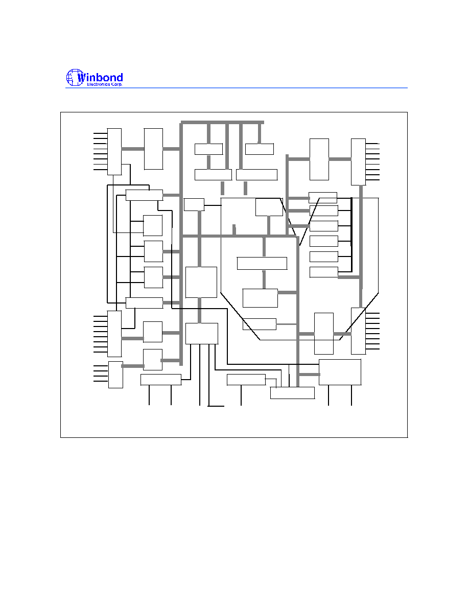
BLOCK DIAGRAM
FUNCTIONAL DESCRIPTION
The W77IC32 is 8052 pin compatible and instruction set compatible. It includes the resources of the
standard 8052 such as four 8-bit I/O Ports, three 16-bit timer/counters, full duplex serial port and
interrupt sources.
The W77IC32 features a faster running and better performance 8-bit CPU with a redesigned core
processor without wasted clock and memory cycles. it improves the performance not just by running
at high frequency but also by reducing the machine cycle duration from the standard 8052 period of
twelve clocks to four clock cycles for the majority of instructions. This improves performance by an
average of 1.5 to 3 times. The W77IC32 also provides dual Data Pointers (DPTRs) to speed up block
Address
Bus
P3.0
P3.7
P1.0
P1.7
ALU
Port 0
Latch
Port 1
Latch
Timer
1
Timer
0
Port
0
Port
1
2 UARTs
XTAL1
PSEN
ALE
GND
V
CC
RST
XTAL2
Oscillator
Interrupt
PSW
Instruction
Decoder
&
Sequencer
Reset Block
Bus & lock
Controller
SFR RAM Address
Power control
&
Power monitor
256 bytes
RAM & SFR
Stack
Pointer
B
Addr. Reg.
Incrementor
PC
Temp Reg.
DPTR 1
T2 Register
T1 Register
ACC
Port 3
Latch
Port
3
P0.0
P0.7
PORT
2
Latch
Port
2
P2.0
P2.7
Timer
2
1KB SRAM
DPTR
Watchdog Timer
Port 4
Latch
Port
4
P4.0
P4.3

Preliminary W77IC32
Publication Release Date: March 2000
- 5 - Revision A0
data memory transfers. It can also adjust the duration of the MOVX instruction (access to off-chip
data memory) between two machine cycles and nine machine cycles. This flexibility allows the
W77IC32 to work efficiently with both fast and slow RAMs and peripheral devices. In addition, the
W77IC32 contains on-chip 1KB MOVX SRAM, the address of which is between 0000H and 03FFH. It
only can be accessed by MOVX instruction; this on-chip SRAM is optional under software control.
The W77IC32 is an 8052 compatible device that gives the user the features of the original 8052
device, but with improved speed and power consumption characteristics. It has the same instruction
set as the 8051 family, with one addition: DEC DPTR (op-code A5H, the DPTR is decreased by 1).
While the original 8051 family was designed to operate at 12 clock periods per machine cycle, the
W77IC32 operates at a much reduced clock rate of only 4 clock periods per machine cycle. This
naturally speeds up the execution of instructions. Consequently, the W77IC32 can run at a higher
speed as compared to the original 8052, even if the same crystal is used. Since the W77IC32 is a
fully static CMOS design, it can also be operated at a lower crystal clock, giving the same throughput
in terms of instruction execution, yet reducing the power consumption.
The 4 clocks per machine cycle feature in the W77IC32 is responsible for a three-fold increase in
execution speed. The W77IC32 has all the standard features of the 8052, and has a few extra
peripherals and features as well.
I/O Ports
The W77IC32 has four 8-bit ports and one extra 4-bit port. Port 0 can be used as an Address/Data
bus when external program is running or external memory/device is accessed by MOVC or MOVX
instruction. In these cases, it has strong pull-ups and pull-downs, and does not need any external pull-
ups. Otherwise it can be used as a general I/O port with open-drain circuit. Port 2 is used chiefly as
the upper 8-bits of the Address bus when port 0 is used as an address/data bus. It also has strong
pull-ups and pull-downs when it serves as an address bus. Port 1 and 3 act as I/O ports with alternate
functions. Port 4 is only available on 44-pin PLCC/QFP package type. It serves as a general purpose
I/O port as Port 1 and Port 3. The P4.0 has an alternate function
WAIT
which is the wait state control
signal. When wait state control signal is enabled, P4.0 is input only.
Serial I/O
The W77IC32 has two enhanced serial ports that are functionally similar to the serial port of the
original 8052 family. However the serial ports on the W77IC32 can operate in different modes in order
to obtain timing similarity as well.
Note that the serial port 0 can use Timer 1 or 2 as baud rate
generator, but the serial port 1 can only use Timer 1 as baud rate generator. The serial ports
have the enhanced features of Automatic Address recognition and Frame Error detection.
Timers
The W77IC32 has three 16-bit timers that are functionally similar to the timers of the 8052 family.
When used as timers, they can be set to run at either 4 clocks or 12 clocks per count, thus providing
the user with the option of operating in a mode that emulates the timing of the original 8052. The
W77IC32 has an additional feature, the watchdog timer. This timer is used as a System Monitor or as
a very long time period timer.
Interrupts
The Interrupt structure in the W77IC32 is slightly different from that of the standard 8052. Due to the
presence of additional features and peripherals, the number of interrupt sources and vectors has been