W78E365 Data Sheet
8-BIT MICROCONTROLLER
Publication Release Date: April 20, 2005
- 1 -
Revision A5
Table of Contents-
1.
GENERAL DESCRIPTION.................................................................................................................. 2
2.
FEATURES ......................................................................................................................................... 2
3.
PIN CONFIGURATIONS ..................................................................................................................... 3
4.
PIN DESCRIPTION ............................................................................................................................. 4
5.
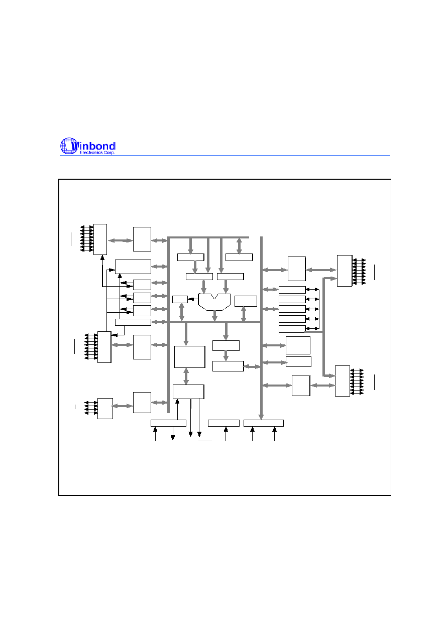
BLOCK DIAGRAM............................................................................................................................... 5
6.
FUNCTIONAL DESCRIPTION ............................................................................................................ 6
6.1
RAM...................................................................................................................................................6
6.2
Timers 0, 1, and 2..............................................................................................................................7
6.3
Clock..................................................................................................................................................7
6.4
Power Management...........................................................................................................................7
6.5
Reset .................................................................................................................................................8
6.6
Port 4 .................................................................................................................................................9
6.7
Pulse Width Modulated Outputs (PWM) ..........................................................................................14
6.8
Watchdog Timer ..............................................................................................................................17
6.9
In-System Programming (ISP) Mode ...............................................................................................19
6.10
Software Reset ................................................................................................................................20
6.11
H/W Reboot Mode (Boot from LDROM) ..........................................................................................21
6.12
Security............................................................................................................................................24
7.
ELECTRICAL CHARACTERISTICS ................................................................................................. 25
7.1
Absolute Maximum Ratings .............................................................................................................25
7.2
D.C. Characteristics.........................................................................................................................25
7.3
A.C. Characteristics .........................................................................................................................27
8.
TIMING WAVEFORMS ..................................................................................................................... 28
8.1
Program Fetch Cycle .......................................................................................................................28
8.2
Data Read Cycle..............................................................................................................................29
8.3
Data Write Cycle..............................................................................................................................30
8.4
Port Access Cycle............................................................................................................................31
9.
TYPICAL APPLICATION CIRCUIT ................................................................................................... 32
9.1
External Program Memory and Crystal ............................................................................................32
9.2
Expanded External Data Memory and Oscillator .............................................................................33
10.
PACKAGE DIMENSIONS ................................................................................................................. 33
10.1
40-pin DIP........................................................................................................................................33
10.2
44-pin PLCC ....................................................................................................................................34
10.3
44-pin PQFP....................................................................................................................................34
11.
APPLICATION NOTE........................................................................................................................ 35
11.1
In-system Programming Software Examples ...................................................................................35
12.
REVISION HISTORY ........................................................................................................................ 40

W78E365
- 2 -
1. GENERAL DESCRIPTION
The W78E365 is an 8-bit microcontroller which has an in-system programmable Flash EPROM for
firmware updating. The instruction set of the W78E365 is fully compatible with the standard 8052. The
W78E365 contains a 64K bytes of main Flash APROM and a 4K bytes of auxiliary Flash LDROM
which allows the contents of the 64KB main APROM to be updated by the loader program located at
the LDROM; 256+1K bytes of on-chip RAM; four 8-bit bi-directional and bit-addressable I/O ports; an
additional 4-bit port P4; three 16-bit timer/counters; a serial port. These peripherals are supported by a
eight sources two-level interrupt capability. To facilitate programming and verification, the ROM inside
the W78E365 allows the program memory to be programmed and read electronically. Once the code
is confirmed, the user can protect the code for security.
The W78E365 microcontroller has two power reduction modes, idle mode and power-down mode,
both of which are software selectable. The idle mode turns off the processor clock but allows for
continued peripheral operation. The power-down mode stops the crystal oscillator for minimum power
consumption. The external clock can be stopped at any time and in any state without affecting the
processor.
2. FEATURES
�
Fully static design 8-bit CMOS microcontroller
�
64K bytes of in-system programmable Flash EPROM for Application Program (APROM)
�
4K bytes of auxiliary ROM for Loader Program (LDROM)
�
256+1K bytes of on-chip RAM. (Including 1K bytes of AUX-RAM, software selectable)
�
Four 8-bit bi-directional ports
�
One 4-bit multipurpose programmable port (I/O, interrupt, Chip select function)
�
Three 16-bit timer/counters
�
One full duplex serial port
�
Watchdog
timer
�
5 channel PWM
�
Software
Reset
�
P1.0 T2 programmable clock out
�
Eight-sources, two-level interrupt capability
�
Built-in power management
�
Code
protection
�
Packaged
in
-
DIP 40: W78E365-40
-
PLCC 44: W78E365P-40
-
QFP 44: W78E365F-40
W78E365
Publication Release Date: April 20, 2005
- 3 -
Revision A5
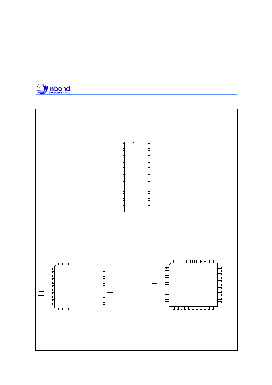
3. PIN CONFIGURATIONS
VDD
1
2
3
4
5
6
7
8
9
10
11
12
13
14
15
16
17
18
19
20
39
40
34
35
36
37
38
30
31
32
33
26
27
28
29
21
22
23
24
25
P0.0, AD0
P0.1, AD1
P0.2, AD2
P0.3, AD3
P0.4, AD4
P0.5, AD5
P0.6, AD6
P0.7, AD7
EA
ALE
PSEN
P2.5, A13
P2.6, A14
P2.7, A15
P2.0, A8
P2.1, A9
P2.2, A10
P2.3, A11
P2.4, A12
T2, P1.0
40-Pin DIP (W78E365)
P1.2
P1.3
P1.4
P1.5
P1.6
RXD, P3.0
TXD, P3.1
P1.7
RST
INT0, P3.2
INT1, P3.3
T0, P3.4
T1, P3.5
WR, P3.6
RD, P3.7
XTAL1
XTAL2
VSS
T2EX, P1.1
44-Pin PLCC (W78E365P)
44-Pin QFP (W78E365F)
40
2
1 44 43 42 41
6
5
4
3
39
38
37
36
35
34
33
32
31
30
29
28
27
26
25
24
23
22
21
20
19
18
17
10
9
8
7
14
13
12
11
16
15
P1.5
P1.6
P1.7
RST
RXD, P3.0
TXD, P3.1
INT0, P3.2
INT1, P3.3
T0, P3.4
T1, P3.5
A
D
3
,
P
0
.
3
T
2
,
P
1
.
0
P
1
.
2
V
D
D
A
D
2
,
P
0
.
2
A
D
1
,
P
0
.
1
A
D
0
,
P
0
.
0
T
2
E
X
,
P
1
.
1
P
1
.
3
P
1
.
4
X
T
A
L
1
V
S
S
P
2
.
4
,
A
1
2
P
2
.
3
,
A
1
1
P
2
.
2
,
A
1
0
P
2
.
1
,
A
9
P
2
.
0
,
A
8
X
T
A
L
2
P
3
.
7
,
/
R
D
P
3
.
6
,
/
W
R
P0.4, AD4
P0.5, AD5
P0.6, AD6
P0.7, AD7
EA
ALE
PSEN
P2.7, A15
P2.6, A14
P2.5, A13
P4.1
P
4
.
0
INT2, P4.3
/
I
N
T
3
,
P
4
.
2
34
40 39 38 37 36 35
44 43 42 41
33
32
31
30
29
28
27
26
25
24
23
P0.4, AD4
P0.5, AD5
P0.6, AD6
P0.7, AD7
EA
ALE
PSEN
P2.7, A15
P2.6, A14
P2.5, A13
22
21
20
19
18
17
16
15
14
13
12
11
4
3
2
1
8
7
6
5
10
9
P1.5
P1.6
P1.7
RST
RXD, P3.0
TXD, P3.1
INT0, P3.2
INT1, P3.3
T0, P3.4
T1, P3.5
X
T
A
L
1
V
S
S
P
2
.
4
,
A
1
2
P
2
.
3
,
A
1
1
P
2
.
2
,
A
1
0
P
2
.
1
,
A
9
P
2
.
0
,
A
8
X
T
A
L
2
P
3
.
7
,
/
R
D
P
3
.
6
,
/
W
R
A
D
3
,
P
0
.
3
T
2
,
P
1
.
0
P
1
.
2
V
D
D
A
D
2
,
P
0
.
2
A
D
1
,
P
0
.
1
A
D
0
,
P
0
.
0
T
2
E
X
,
P
1
.
1
P
1
.
3
P
1
.
4
P
4
.
0
/
I
N
T
3
,
P
4
.
2
P4.1
INT2, P4.3
W78E365
- 4 -
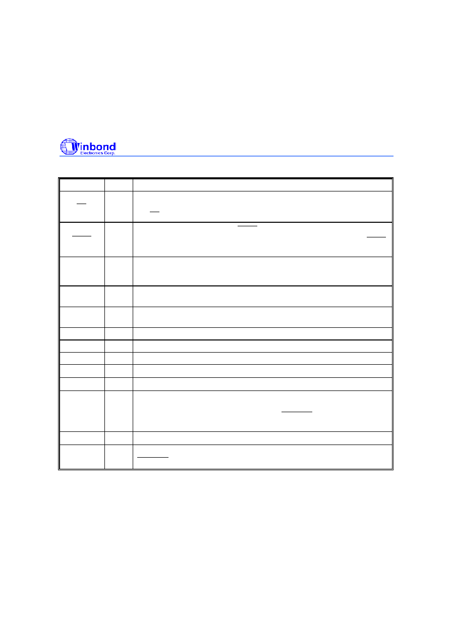
4. PIN DESCRIPTION
SYMBOL TYPE
DESCRIPTIONS
EA
I
EXTERNAL ACCESS ENABLE: This pin forces the processor to execute the
external ROM. The ROM address and data will not be presented on the bus if
the EA pin is high.
PSEN
O H
PROGRAM STORE ENABLE: PSEN enables the external ROM data in the
Port 0 address/data bus. When internal ROM access is performed, no PSEN
strobe signal outputs originate from this pin.
ALE O
H
ADDRESS LATCH ENABLE: ALE is used to enable the address latch that
separates the address from the data on Port 0. ALE runs at 1/6th of the
oscillator frequency.
RST
I L
RESET: A high on this pin for two machine cycles while the oscillator is
running resets the device.
XTAL1 I
CRYSTAL 1: This is the crystal oscillator input. This pin may be driven by an
external clock.
XTAL2
O
CRYSTAL 2: This is the crystal oscillator output. It is the inversion of XTAL1.
V
SS
I
GROUND: ground potential.
V
DD
I
POWER SUPPLY: Supply voltage for operation.
P0.0
-
P0.7 I/O D PORT 0: Function is the same as that of standard 8052.
P1.0
-
P1.7 I/O H PORT 1: Function is the same as that of standard 8052.
P2.0
-
P2.7 I/O H
PORT 2: Port 2 is a bi-directional I/O port with internal pull-ups. This port also
provides the upper address bits for accesses to external memory. The P2.6
and P2.7 also provide the alternate function REBOOT which is H/W reboot
from LD flash.
P3.0
-
P3.7 I/O H PORT 3: Function is the same as that of the standard 8052.
P4.0
-
P4.7 I/O H
PORT 4: A bi-directional I/O. The P4.3 also provides the alternate function
REBOOT
which is H/W reboot from LD flash.
* Note: TYPE I: input, O: output, I/O: bi-directional, H: pull-high, L: pull-low, D: open drain