
Winbond
ACPI-STR Controller
W83301DR-O
W83301DR-O
Data Sheet Revision History
Pages Dates Version Version
on Web
Main Contents
1
N.A.
02/Jul.
1.0
1.0
1
st
Release
Please note that all data and specifications are subject to change without notice.
All the trademarks of products and companies mentioned in this datasheet
belong to their respective owners.
LIFE SUPPORT APPLICATIONS
These products are not designed for use in life support appliances, devices, or
systems where malfunction of these products can reasonably be expected to
result in personal injury. Winbond customers using or selling these products for
use in such applications do so at their own risk and agree to fully indemnify
Winbond for any damages resulting from such improper use or sales.

Publication Release Date: Jul., 2002
Revision 1.0
1
W83301DR-O
1. General Description
The W83301DR-O is an ACPI-compliant controller for microprocessor and other
computer applications. The part provides functions - two switch controllers to generate a
5V
DL
and a 3.3 V
DL
voltage from ATX power supply; a linear controller � STR1 (2.5V
DUAL
),
and a bus termination controller � STR2 (1.25 V
DUAL
) for high-speed bus such as
RDRAM/DDRAM current sinking and sourcing. Besides, the W83301DR-O also can
provide extra voltage up to 0.4V in each regulator output for over-clocking application and
more performance by two hardware pins - V
SET2
, and V
SET3
. In order to reduce the
customer's cost, and simplify the circuit design, the W83301DR-O integrates a charge-
pump engine into the chip to provide higher driving voltage to drive single N-channel
MOSFETs. The W83301DR-O also offers PWOK and over current detection to protect
each output and soft-start protects all linear controllers from rush current attack. The
W83301DR-O is available in a 24-pin TSSOP package.
2. Features
v
Provides various voltages for DDR-STR applications
�
Provide a switch controller to generate 5V
DUAL
voltage
�
Provide a switch controller to generate 3.3V
DUAL
voltage
�
Linear controller STR1�2.5V
DUAL
for DDR application
�
Bus termination controller STR2 �1.25V
DUAL
for high speed bus termination
to sink and drive redundant current
v
Provide a switch 5V
DLEN
pin to enable/disable 5V
DL
output in S5 state for USB
application
v
Supports DDR ACPI-STR Functions
v
Drives all N-Channel MOSFETs
v
Power-Up Softstart for all controllers
v
Up to 0.4V/0.2V incremental voltage on STR1/STR2 for over-clocking application.
v
Under-Voltage Fault Monitor
v
Soft-Start function
v
24-Pin TSSOP Package
Publication Release Date: Jul., 2002
Revision 1.0
2
W83301DR-O
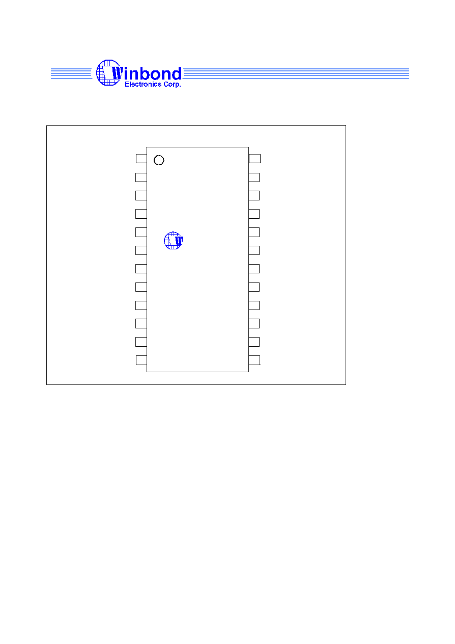
3. W83301DR-O Pin Configuration
BT
DRV
BT
SEN
BT
SINK
Reserved
Vss
5V
SB
C1
C2
ChrPmp
STR1
DRV
STR1
SEN
SS
PWOK
3V
DRV
/5V
DRV
5V
DLSB
3V
DLSB
3V
SBSEN
2
3
4
5
6
7
8
9
10
11
23
22
21
20
19
18
17
16
15
14 S5#
S3#
5V
DLEN
#
Reserved
Reserved
1
24
12
13 V
SET2
V
SET3
inbond
W83301DR-O
Publication Release Date: Jul., 2002
Revision 1.0
3
W83301DR-O
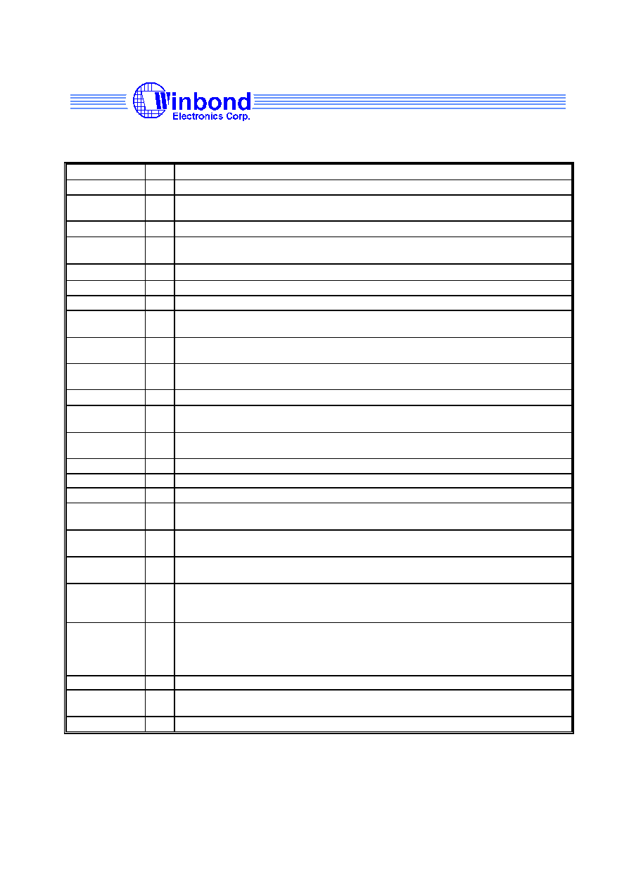
4. Pin Description
SYMBOL
PIN
FUNCTION
Reserved
1
Pin Reserved
BT
DRV
2
BT Current Source. Connect this pin to the gate of a suitable N-channel
MOSFET for driving bus termination regulator output.
BT
SEN
3
BT Sense. Connect this pin to the bus termination regulator output.
BT
SINK
4
BT Current Sink. This pin is used to drive a N-channel MOSFET to sink the
redundant current in the high-speed bus.
Reserved
5
Function Reserved. Pull up this pin to +5VSB through a 1.5 Kohm resistor.
Vss
6
Power Ground. Connect this pin to ground.
5V
SB
7
Power 5V
SB
. Input 5V
SB
supply.
C1
8
Charge Pump Cap. Attach flying capacitor between this pin and C2 to
generate internally used high voltage from 5V power supply.
C2
9
Charge Pump Cap. Attach flying capacitor between this pin and C1 to
generate internally used high voltage from 5V power supply.
ChrPmp
10
Charge Pump output. This pin produces voltage doubled 5V supply by
charge pumping. Bypass with a 0.1uF capacitor.
5V
DLEN
#
11
5VDL Enable. Control 5V
DL
voltage output. Pull-up internally.
V
SET3
12
Voltage Selection. Combine with VSET2 to select output voltages of STR
regulators.
V
SET2
13
Voltage Selection. Combine with VSET3 to select output voltages of STR
regulators.
S5#
14
S5 Signal. Control signal governing the soft off state S5. Pull-up internally.
S3#
15
S3 Signal. Control signal governing the soft off state S3. Pull-up internally.
3V
SBSEN
16
3V
DL
Sense. Connect this pin to the STR1 output.
3V
DLSB
17
3V
DL
Drive. Connect this pin to the gate of a suitable N-channel MOSFET for
driving STR1 output.
5V
DLSB
18
5VSB Output Control. Connect this pin to the gate of a N-MOSFET to output
5VSB power to 5V
DL
.
3V
DRV
/5V
DRV
19
3.3V/5V Output Control. Connect this pin to the gate of a N-MOSFET to
output 3.3V/5V power to 3.3V
DL
/5V
DL
.
PWOK
20
Power OK. Open collector input/output. Used to indicate the ready of 5Vin
supply. If any STR supply occurs over current and induce under-voltage,
PWOK will be pull down.
SS
21
Soft-Start. Attach a capacitor (0.033u) to this pin to determine the softstart
rate. A ramp generated by charging this capacitor with internal soft-start
current (18uA) is used to clamp the voltage rising slew rate of STR regulators
and 5V
DL
. Soft starting avoids too much rush current during voltage setup.
STR1
SEN
22
STR1 Sense. Connect this pin to the STR1 output.
STR1
DRV
23
STR1 Drive. Connect this pin to the gate of a suitable N-channel MOSFET for
driving STR1 output.
Reserved
24
Pin Reserved