
W83791D
Winbond H/W
Monitoring IC
W83791D
Preliminary
Publication Release Date: Aug, 2001
Revision 0.41
i
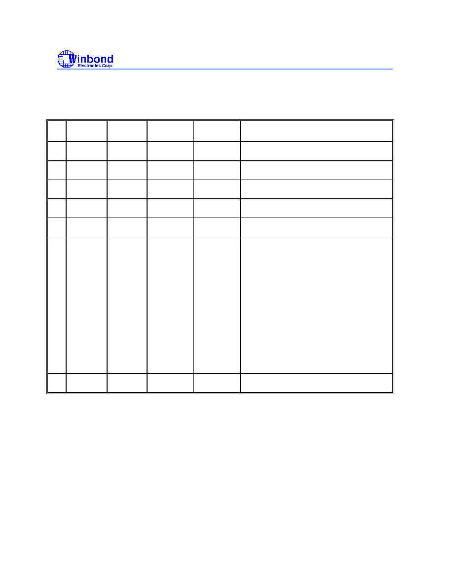
W83791D Data Sheet Revision History
Pages
Dates
Version
Version
on Web
Main Contents
1
n.a.
n.a.
All version before 0.20 are for internal use.
2
n.a.
01/Jan
0.2
n.a.
First publication.
3
P.7
01/Jan
0.21
n.a.
Revise SLOTOCC# pin description.
4
P.34
01/Jan
0.21
n.a.
Add SMI# /IRQ for Voltage/Fan description.
5
P.43/44
19/Mar
0.3
n.a.
Register Index 1Ah~1Fh revised.
6
P. 40
P. 42
P. 60/61
P. 58/59
P. 66
P. 66
P. 66
P. 87
21/May
0.4
n.a.
This update is for C version IC.
1) Add EVNTRAP1-5 polarity (Index Ah )
2) Add VID protection control bit (Index15h
bit5)
3) Add FAN1-3/PWMOUT1-3 as GPIn data
register. (Index 95h/97h)
4) SMARTFAN
TM
step up/down time registers
exchanged.
5) Add a bit (Index A6 bit7) to know either
speech or GPIO function did you use.
6) Pin44 (SMI#/LEDOUT) is a multi-function,
it is programmable.
7) EVENTRAP can as GPIO by programming
Index A6h bit0-4 .
8) Updated V0.17 schematics adding
LEDOUT circuit for SMI# (Pin 44)
7
All pages
09/Aug
0.41
n.a.
Repaginate datasheet
Please note that all data and specifications are subject to change without notice. All the
trademarks of products and companies mentioned in this data sheet belong to their respective
owners.
LIFE SUPPORT APPLICATIONS
These products are not designed for use in life support appliances, devices, or systems where
malfunction of these products can reasonably be expected to result in personal injury. Winbond
customers using or selling these products for use in such applications do so at their own risk and
agree to fully indemnify Winbond for any damages resulting from such improper use or sales.

W83791D
Preliminary
Publication Release Date: Aug, 2001
Revision 0.41
ii
TABLE OF CONTENTS
1.
GENERAL DESCRIPTION .................................................................................................... 1
2.
FEATURES ........................................................................................................................... 3
2.1
Monitoring Items .................................................................................................................................3
2.2
Address Resolution Protocol (ARP) and Alert-Standard Forum(ASF)...................................................3
2.3
Speech Items .......................................................................................................................................3
2.4
Actions Enabling .................................................................................................................................3
2.5
Enhance Monitoring VID function .......................................................................................................4
2.6
General................................................................................................................................................4
2.7
Package ...............................................................................................................................................4
3.
KEY SPECIFICATIONS......................................................................................................... 4
4.
PIN CONFIGURATION .......................................................................................................... 5
5.
PIN DESCRIPTION................................................................................................................ 6
6.
FUNCTION DESCRIPTION.................................................................................................. 10
6.1
General Description ...........................................................................................................................10
6.2
Access Interface ................................................................................................................................10
6.2.1
The first serial bus access timing ............................................................................ 10
6.3
Speech Function ................................................................................................................................11
6.3.1
General Description ................................................................................................. 11
6.3.2
Event Trigger Queue ............................................................................................... 11
6.3.3
Connection of EEPROM .......................................................................................... 12
6.3.4
Speaker Output ....................................................................................................... 13
6.4
Address Resolution Protocol (ARP) Introduction ...............................................................................14
6.5
ASF(Alert Standard Format) Introduction ..........................................................................................16
6.5.1
Platform Event Trap (PET)....................................................................................... 16
6.6
Analog Inputs ....................................................................................................................................19
6.6.1
Monitor over 4.096V voltage: ................................................................................... 19
6.6.2
Monitor negative voltage:......................................................................................... 20
6.7
FAN Speed Count and FAN Speed Control........................................................................................21
6.7.1
Fan speed count...................................................................................................... 21
6.7.2
Fan speed control.................................................................................................... 22
6.7.3
Smart Fan Control ................................................................................................... 23
6.8
Temperature Measurement Machine ..................................................................................................25
6.8.1
Monitor temperature from thermistor: ....................................................................... 25
6.8.2
Monitor temperature from Pentium II
TM
thermal diode or bipolar transistor 2N3904... 25
6.8.3
SMI# interrupt for W83791D Voltage........................................................................ 26
6.8.4
SMI# interrupt for W83791D Fan ............................................................................. 26
6.8.5
SMI# interrupt for W83791D temperature sensor 1/2/3 ................................................................................................

W83791D
Preliminary
Publication Release Date: Aug, 2001
Revision 0.41
iii
6.8.6
Over-Temperature (OVT#) for W83791D temperature sensor 1/2/3.......................... 28
7
CONTROL AND STATUS REGISTER........................ ERROR! BOOKMARK NOT DEFINED.
7.1
Speech Flash Memory Address Registers
Index 00h-02h (Bank 0)... Error! Bookmark not defined.
7.2
Speech Flash Memory Data Registers
Index 03h-06h (Bank 0) ........ Error! Bookmark not defined.
7.3
Speech Flash Memory Control Register
Index 07h (Bank 0) ............ Error! Bookmark not defined.
7.4
Event Trigger Timeout Register
Index 08h (Bank 0)........................ Error! Bookmark not defined.
7.5
Speech Programmable Trigger Register
Index 09h (Bank 0) ............ Error! Bookmark not defined.
7.6
Speech Input Trigger Property Register
Index 0Ah (Bank 0)............ Error! Bookmark not defined.
7.7
Reserved Register
Index 0Bh (Bank 0) ............................................ Error! Bookmark not defined.
7.8
VID and VCORE voltage Property Register
Index 0Ch (Bank 0) ..... Error! Bookmark not defined.
7.9
Speech Flash Memory Read Data Registers
Index 0Dh-0Eh (Bank 0)Error! Bookmark not defined.
7.10
Reserved Register
Index 0Fh (Bank 0) ............................................ Error! Bookmark not defined.
7.11
VID Control/Status Register
Index 10h (Bank 0) ............................. Error! Bookmark not defined.
7.12
Entry Disable VID Output Control Register
Index 11h (Bank 0) ...... Error! Bookmark not defined.
7.13
VID Output Tolerance/Limit Register
Index 12h (Bank 0) ............... Error! Bookmark not defined.
7.14
GPIO Control Register I
Index 13h (Bank 0) ................................... Error! Bookmark not defined.
7.15
GPIO Data/Status Register I
Index 14h (Bank 0) ............................. Error! Bookmark not defined.
7.16
GPIO Control Register II
Index 15h (Bank 0).................................. Error! Bookmark not defined.
7.17
GPIO Output Data and Status Register II
Index 16h (Bank 0) .......... Error! Bookmark not defined.
7.18
LED Control Register
Index 17h (Bank 0)....................................... Error! Bookmark not defined.
7.19
User Defined Registers
Index 18h-1Ch (Bank 0) ............................. Error! Bookmark not defined.
7.20
Speech Control Register 1-- Index 1Dh (Bank 0).................................. Error! Bookmark not defined.
7.21
Speech Control Register 2-- Index 1Eh (
Bank 0) .................................. Error! Bookmark not defined.
7.22
Speech Control Register 3-- Index 1Fh (
Bank 0)................................... Error! Bookmark not defined.
7.23
Value RAM
Index 20h- 3Fh (Bank 0).............................................. Error! Bookmark not defined.
7.24
Configuration Register
Index 40h (Bank 0) ..................................... Error! Bookmark not defined.
7.25
Interrupt Status Register 1
Index 41h (Bank 0) ................................ Error! Bookmark not defined.
7.26
Interrupt Status Register 2
Index 42h (Bank 0) ................................ Error! Bookmark not defined.
7.27
SMI# Mask Register 1
Index 43h (Bank 0)...................................... Error! Bookmark not defined.
7.28
SMI# Mask Register 2
Index 44h (Bank 0)...................................... Error! Bookmark not defined.
7.29
IRQ Mask Register 1
Index 45h (Bank 0) ........................................ Error! Bookmark not defined.
7.30
IRQ Mask Register 2
Index 46h (Bank 0) ........................................ Error! Bookmark not defined.
7.31
VID/Fan Divisor Register
Index 47h (Bank 0) ................................. Error! Bookmark not defined.
7.32
Serial Bus Address Register
Index 48h (Bank 0).............................. Error! Bookmark not defined.
7.33
Voltage ID (VID4) & Device ID -- Index 49h (Bank 0) ........................ Error! Bookmark not defined.
7.34
Temperature 2 and Temperature 3 Serial Bus Address Register -- Index4Ah (Bank 0)Error! Bookmark
not defined.
7.35
Pin Control Register -- Index4Bh (Bank 0)........................................... Error! Bookmark not defined.
7.36
SMI#/OVT# Property Select -- Index 4Ch (Bank 0) ............................. Error! Bookmark not defined.
7.37
FAN 1- 3 IN/OUT and BEEP Control Register -- Index 4Dh (Bank 0).. Error! Bookmark not defined.
7.38
Bank Select -- Index 4Eh (Bank 0) ....................................................... Error! Bookmark not defined.
7.39
Winbond Vendor ID -- Index 4Fh (Bank 0) .......................................... Error! Bookmark not defined.
7.40
Winbond Test Register -- Index 50h - 55h (Bank 0).............................. Error! Bookmark not defined.
7.41
BEEP Control Register 1-- Index 56h (Bank 0) .................................... Error! Bookmark not defined.

W83791D
Preliminary
Publication Release Date: Aug, 2001
Revision 0.41
iv
7.42
BEEP Control Register 2-- Index 57h (
Bank 0)..................................... Error! Bookmark not defined.
7.43
Chip ID -- Index 58h (
Bank 0) ............................................................. Error! Bookmark not defined.
7.44
Diode Selection Register -- Index 59h (Bank 0)................................... Error! Bookmark not defined.
7.45
Reserved -- Index 5Ah - (
Bank 0)........................................................ Error! Bookmark not defined.
7.46
FANIN 4/5 Control -- Index 5Bh (Bank 0) .......................................... Error! Bookmark not defined.
7.47
FAN 4/5 Divisor Control -- Index 5Ch (Bank 0)................................. Error! Bookmark not defined.
7.48
VBAT Monitor Control Register -- Index 5Dh (
Bank 0) ....................... Error! Bookmark not defined.
7.49
ACPI Temperature Increment Register -- Index 5Eh............................. Error! Bookmark not defined.
7.50
Reserved -- Index 5Fh (
Bank 0)........................................................... Error! Bookmark not defined.
7.51
FAN 1 Pre-Scale Register-- Index 80h
(Bank 0) ................................... Error! Bookmark not defined.
7.52
FAN 1 Duty Cycle Select Register-- 81h (
Bank 0)................................ Error! Bookmark not defined.
7.53
FAN 2 Pre-Scale Register-- Index 82h
(Bank 0) ................................... Error! Bookmark not defined.
7.54
FAN2 Duty Cycle Select Register-- Index 83h
(Bank 0) ....................... Error! Bookmark not defined.
7.55
FAN 1/2 Configuration Register-- Index 84h
(Bank 0).......................... Error! Bookmark not defined.
7.56
Fan 1 Target Temperature Register/Target Fan 1 Speed Control Register -- Index 85h
(Bank 0)...Error!
Bookmark not defined.
7.57
Fan 2 Target Temperature Register/Target Fan 2 Speed Control Register-- Index 86h
(Bank 0)....Error!
Bookmark not defined.
7.58
Tolerance of Fan1/2 Target Temperature or Speed Register -- Index 87h
(Bank0)Error! Bookmark not
defined.
7.59
Fan 1 PWM Stop Duty Cycle Register -- Index 88h
(Bank 0)................ Error! Bookmark not defined.
7.60
Fan 2 PWM Stop Duty Cycle Register -- 89h (
Bank 0) ......................... Error! Bookmark not defined.
7.61
Fan 1 Start-up Duty Cycle Register -- Index 8Ah
(Bank 0) ................... Error! Bookmark not defined.
7.62
Fan 2 Start-up Duty Cycle Register -- Index 8Bh
(Bank 0).................... Error! Bookmark not defined.
7.63
Fan 1 Stop Time Register -- Index 8Ch
(Bank 0) .................................. Error! Bookmark not defined.
7.64
Fan 2 Stop Time Register -- Index 8Dh
(Bank 0).................................. Error! Bookmark not defined.
7.65
Fan 1/2/3 Step Down Time Register -- Index 8Eh
(Bank 0)................... Error! Bookmark not defined.
7.66
Fan 1/2/3 Step Up Time Register -- Index 8Fh
(Bank 0) ....................... Error! Bookmark not defined.
7.67
Temperature Sensor 1 (VTIN1) Offset Register - Index 90h
(Bank 0) ... Error! Bookmark not defined.
7.68
Temperature Sensor 2 (VTIN2) Offset Register - Index 91h
(Bank 0) ... Error! Bookmark not defined.
7.69
Temperature Sensor 3 (VTIN3) Offset Register - Index 92h
(Bank 0) ... Error! Bookmark not defined.
7.70
FAN 3 Pre-Scale Register-- Index 93h
(Bank 0) ................................... Error! Bookmark not defined.
7.71
FAN 3 Duty Cycle Select Register-- 94h (
Bank 0)................................ Error! Bookmark not defined.
7.72
FAN 3 Configuration Register-- Index 95h
(Bank 0)............................. Error! Bookmark not defined.
7.73
Fan 3 Target Temperature Register/Target Fan 3 Speed Control Register -- Index 96h
(Bank 0)...Error!
Bookmark not defined.
7.74
Tolerance of Fan 3 Target Temperature or Speed Register -- Index 97h
(Bank 0)Error! Bookmark not
defined.
7.75
Fan 3 PWM Stop Duty Cycle Register -- Index 98h
(Bank 0)................ Error! Bookmark not defined.
7.76
Fan 3 Start-up Duty Cycle Register -- Index 99h
(Bank 0) .................... Error! Bookmark not defined.
7.77
Fan 3 Stop Time Register -- Index 9Ah
(Bank 0).................................. Error! Bookmark not defined.
7.78
Interrupt Status Register III -- Index 9Bh
(Bank 0) ............................... Error! Bookmark not defined.
7.79
SMI# Mask Register III -- Index 9Ch
(Bank 0)..................................... Error! Bookmark not defined.
7.80
Interrupt Mask Register III -- Index 9Dh
(Bank 0)................................ Error! Bookmark not defined.
7.81
FAN4_PRE_SCALE register-- Index 9Eh (
Bank 0).............................. Error! Bookmark not defined.
7.82
FAN5_PRE_SCALE register-- Index 9Fh (
Bank 0).............................. Error! Bookmark not defined.