
W83L785TS-S
Winbond H/W Monitoring IC
W83L785TS-S
Preliminary
W83L785TS-S
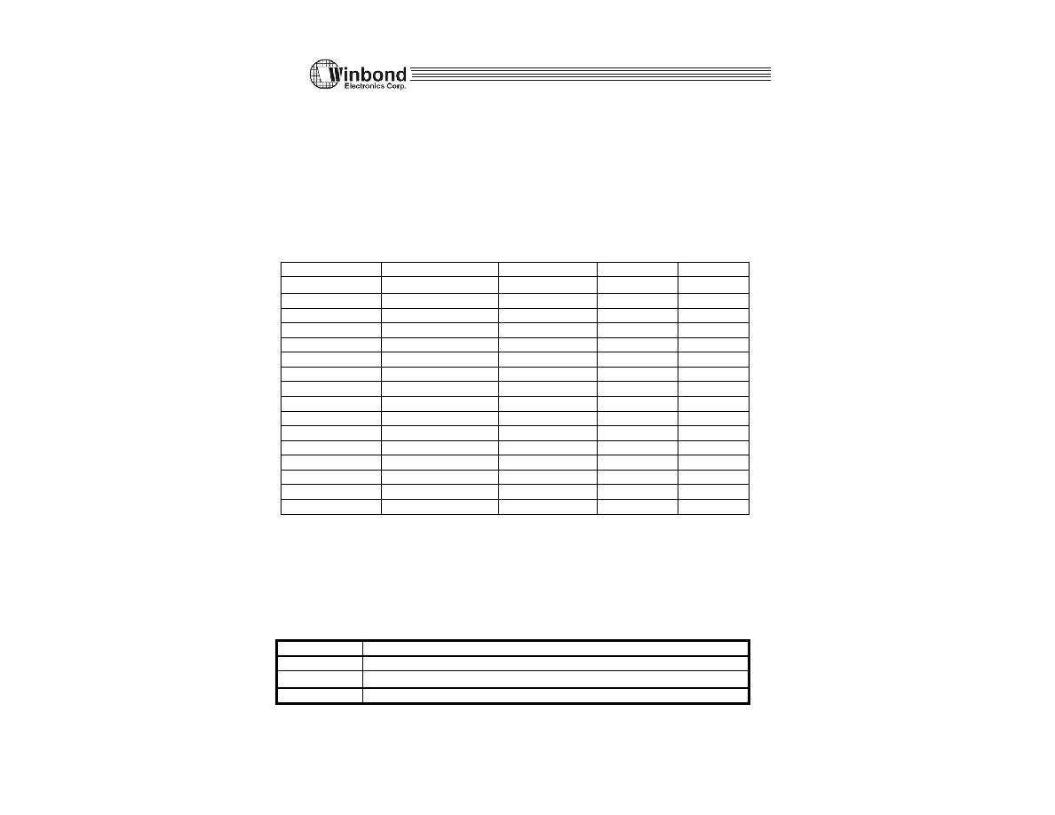
Data Sheet Revision History
Pages Dates Versio
n
Version
on Web
Main Contents
1
n.a.
n.a.
All the version before 0.50 are for internal
use.
2
3
4
5
6
7
8
Please note that all data and specifications are subject to change without notice. All the trade
marks of products and companies mentioned in this data sheet belong to their respective owners.
LIFE SUPPORT APPLICATIONS
These products are not designed for use in life support appliances, devices, or systems where
malfunction of these products can reasonably be expected to result in personal injury. Winbond
customers using or selling these products for use in such applications do so at their own risk and
agree to fully indemnify Winbond for any damages resulting from such improper use or sales.
Publication Release Date: April 2002
Revision 0.5
2

W83L785TS-S
Preliminary
TABLE OF CONTENTS
1. GENERAL DESCRIPTION.......................................................................... 5
2. FEATURES................................................................................................... 5
3. KEY SPECIFICATIONS............................................................................... 5
4. PIN CONFIGURATION .............. ERROR! BOOKMARK NOT DEFINED.6
5. PIN DESCRIPTION...................................................................................... 6
6.. FUNCTIONAL DESCRIPTION................................................................... 7
6.1 General
Description......................................................... Error! Bookmark not defined.
6.2 Access
Interface................................................................................................................ 7
6.2.1 The first serial bus access timing are shown as follow:................................................... 7
6.3 Analog
Inputs ................................................................................................................... 8
6.3.1 Temperature Measurement Machine ............................................................................. 8
6.3.2 Monitor temperature from thermal diode ....................................................................... 8
6.4 OFFSET and Temperature Fault Limit (FAULT_LIMIT) Setting ................................... 9
6.5 TEMP_FAULT#
............................................................................................................ 10
7. CONTENT OF DATA REGISTERS .......................................................... 11
7.1 Configuration
Register
Index 40h ............................................................................. 11
7.2 Reserved
--Index
41h~4Bh ............................................................................................. 11
7.3 Winbond Vendor ID (Low Byte) - Index 4Ch (Auto Increase)....................................... 11
7.4 Winbond Vendor ID (High Byte) - Index 4Dh (No Auto Increase)................................ 11
7.5 Chip ID -- Index 4Eh...................................................................................................... 12
7.6 Reserved -- Index 4Fh~51h ............................................................................................ 12
7.7 Thermal Sensor 1/2 Type Register -- Index 52h............................................................. 12
7.8 Temperature 1 Fault Limit -- Index 53h......................................................................... 12
7.9 Reserved
--Index
54h~84h) ............................................................................................ 13
7.10 Temperature 1 OFFSET Register-- Index 85h............................................................... 13
8. VALUE RAM AND LIMIT VALUE ........................................................... 13
8.1 Value
RAM
Index 20h- 3Fh....................................................................................... 13
9. SPECIFICATIONS..................................................................................... 14
9.1 Absolute
Maximum
Ratings............................................................................................ 14
9.2 DC
Characteristics......................................................................................................... 14
9.3 AC
Characteristics ......................................................................................................... 16
10. HOW TO READ THE TOP MARKING................................................... 17
11. PACKAGE DRAWING AND DIMENSIONS.......................................... 18
Publication Release Date: April 2002
Revision 0.5
3

W83L785TS-S
Preliminary
12. W83L785TR SCHEMATICS..................................................................... 19
Publication Release Date: April 2002
Revision 0.5
4

W83L785TS-S
Preliminary
1. GENERAL DESCRIPTION
The W83L785TS-S a low-cost, fully integrated temperature sensor issues an alert signal when the
monitoring temperature exceeds the threshold. The W83L785TS-S provides 1 remote temperature
sensing connected to CPU thermal diode. There is one dedicated OFFSET/ FAULT_LIMIT pin
to compensate inaccuracy of CPU temperature measurement by adjusting external two serial
resistors and set up temperature fault threshold. When W83L785TS-S begins monitoring, the
Watch Dog machine monitors every function and store the value to registers. If the monitored
value exceeds the limit value, the interrupt status will be set to 1.The W83L785TS-S
communicates over a two-wire serial interface compatible with SMBus standards.
2. FEATURES
�
Low Cost
�
1 thermal inputs for remote CPU thermal diode
�
WATCHDOG comparison of all monitored values
�
Auto Protection When Over Temperature
�
I
2
C
TM
serial bus interface
�
2.7~5.5V Supply
�
8-pin SOP (150mil)
3. KEY SPECIFICATIONS
�
Monitoring Temperature Range and Accuracy
- 40
�
C to +120
�
C
�
3
�
C(Max)
�
Supply Voltage
2.7V ~ 5.5V
�
Operating Supply Current
2 mA typ.
�
ADC Resolution
8 Bits
Publication Release Date: April 2002
Revision 0.5
5
W83L785TS-S
Preliminary
4. PIN CONFIGURATION
8
7
6
5
1
2
3
4
SCL
SDA
GND
TEMP_FAULT#
OFFSET/FAULT_LIMIT
VREF
CPUT
VDD
785TS-S
5. PIN DESCRIPTION
I/O
- TTL level bi-directional pin with 12 mA source-sink capability,open drain output
12t
I/O
12ts
- TTL level and schmitt trigger
OUT
12
- Output pin with 12 mA source-sink capability
AOUT - Output pin(Analog)
OD
- Open-drain output pin with 12 mA sink capability
12
IN
t
- TTL level input pin
IN
ts
- TTL level input pin and schmitt trigger
AIN
- Input pin(Analog)
PIN NAME
PIN NO.
TYPE
DESCRIPTION
VDD
1
POWER
+3.3 VDD (or 3.3VSB) power supply input.
CPUT
2
AIN
CPU thermal diode input.
VREF 3
AOUT
Reference
Voltage.
OFFSET/
FAULT_LIMIT
4
VIN
This pin can be used to change CPUT offset value and set
up the temperature_fault limit.by adjusting two external
serial resistors.
GND
5
Ground Ground.
TEMP_FAULT# 6
OD
12
Active-Low output. This pin will be a logic LOW when
CPU temperature exceeds limit.
SDA 7
I/OD
12
Serial Bus bi-directional Data.
SCL 8
IN
t s
Serial Bus Clock.
Publication Release Date: April 2002
Revision 0.5
6
W83L785TS-S
Preliminary
6. FUNCTIONAL DESCRIPTION
6.1 General Description
The W83L785TS-S a low-cost, fully integrated temperature sensor issues an alert signal when the
monitoring temperature exceeds the threshold. The W83L785TS-S provides 1 remote temperature
sensing connected to CPU thermal diode. There is 1 dedicated OFFSET/ FAULT_LIMIT pin to
compensate inaccuracy of CPU temperature by adjusting external two serial resistors and set up
temperature fault threshold. When W83L785TS-S starts the monitor function on the chip, the
Watch Dog machine monitor every function and store the value to registers. If the monitor value
exceeds the limit value, the interrupt status will be set to 1.
6.2 Access Interface
The W83L785TS-S provides I
2
C Serial Bus to read/write internal registers. In the W83L785TS-S,
the I2C address defined value is 0101110.
6.2.1 The first serial bus access timing are shown as follow:
(a)
Serial bus write to internal address register followed by the data byte
0
Start By
Master
0
1
0
1
1
1
D7
D6
D5
D4
D3
D2
D1
D0
Ack
by
785TR
R/W
Ack
by
785TR
SCL
SDA
D7
D6
D5
D4
D3
D2
D1
D0
Ack
by
785TR
Stop
by
Master
SCL
SDA (Continued)
7
8
0
7
8
0
7
8
Frame 2
Internal Index Register Byte
(Continued)
Frame 3
Data Byte
Frame 1
Serial Bus Address Byte
Figure 1. Serial Bus Write to Internal Address Register followed by the Data Byte
0
Publication Release Date: April 2002
Revision 0.5
7
W83L785TS-S
Preliminary
(b)
Serial bus read form internal address register followed by the data byte
0
Repeat start
by Master
0
1
0
1
1
0
1
D7
D6
D5
D4
D3
D2
D1
D0
ack
by
785TR
R/W
ack
by
785TR
D7
D6
D5
D4
D3
D2
D1
D0
Ack
by
784R
Stop by
Master
7
8
0
7
8
Frame 2
Internal Index Register Byte
Frame 4
Data Byte from 785TR
Frame 1
Serial Bus Address Byte
Figure 2. Serial Bus read from Internal Address Register followed by the Data Byte
0
1
2
3
4
5
6
7
8
0
1
3
4
5
2
6
7
1
0
1
1
0
0
1
R/W
8
Nack
by
Master
Frame 3
Serial Bus Byte
ack
by
785TR
SCL
SDA
SCL(Continued)
SDA(Continued)
6.3 Analog Inputs
6.3.1 Temperature measurement machine
The W83L785TS-S provides a best solution to prevent CPU from being damaged. The
temperature data format is 8-bit two-complement for thermal sensor. The 8-bit temperature data
can be obtained by reading the register. The format of the temperature data is show in Table 1.
Table 1: The format of the temperature data
Temperature
8-Bit Digital Output
8-Bit Binary
8-Bit Hex
+125
�
C
0111,1101 7Dh
+25
�
C
0001,1001 19h
+2
�
C
0000,0010 02h
+1
�
C
0000,0001 01h
+0
�
C
0000,0000 00h
-1
�
C
1111,1111 FFh
-2
�
C
1111,1110 FEh
-25
�
C
1110,0111 E7h
-55
�
C
1100,1001 C9h
Publication Release Date: April 2002
Revision 0.5
8
W83L785TS-S
Preliminary
6.3.2
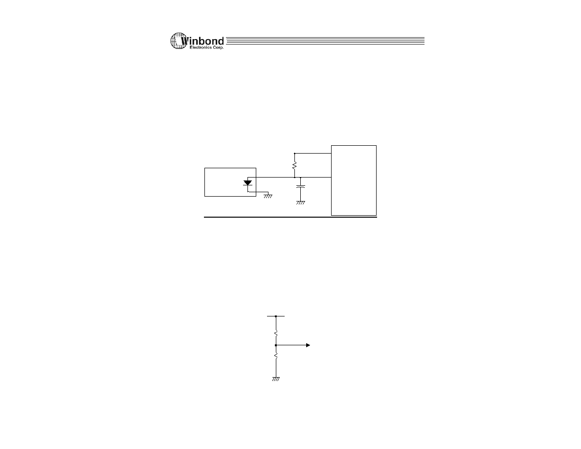
Monitor temperature from thermal diode :
The W83L785TS-S can monitor the temperature from the thermal diode and issue
temperature fault signal to activate system protection when temperature exceeds the threshold.
The terminators of thermal diode are connected to power supply ground (GND) and the
CPUT(pin2) in the W83L785TS-S. The resistor R=15K ohms should be connected to VREF
to supply the diode bias current
R=15K, 1%
C=3300pF
VREF
CPUT1
W83L785TS-S
D+
D-
Therminal
Diode
Microprocessor
Figure 3
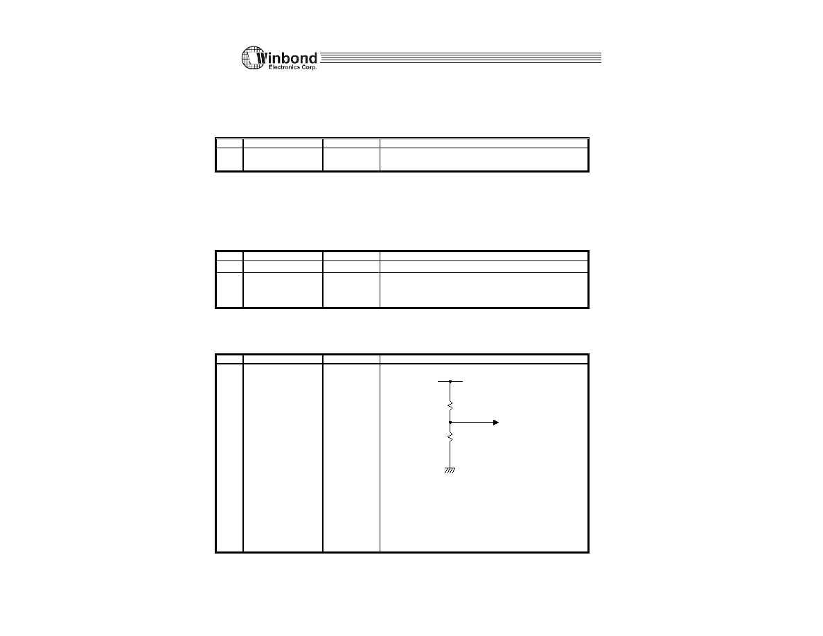
6.4 OFFSET and Temperature Fault Limit (FAULT_LIMIT) Setting
There is one dedicated pin to change the offset value and temperature fault limited value by
adjusting external serial resistors. By adjusting external resistors, there are two sets of
temperature fault limit to be chosen and they are 85,90
o
C. As for the application circuit and
corresponding resistors value, please see the figure and table as below.
R1
R2
OFFSET
VREF
Figure 4: OFFSET Setting
Publication Release Date: April 2002
Revision 0.5
9
W83L785TS-S
Preliminary
Table 2: The CPU OFFSET value and Temperature Fault Limited Value
TFAULT_LIMIT
OFFSET
R1 R2
0000XXXX 85 0
X
10K
0001XXXX 85 22
91K
9.1K
0010XXXX 85 24
30K
5.6K
0011XXXX 85 26
20K
5.6K
0100XXXX 85 28
13K
5.1K
0101XXXX 85 30
91K
4.7K
0110XXXX 85 32
68K
4.7K
0111XXXX 85 34
18K
16K
1000XXXX 90 0
16K
18K
1001XXXX 90 22
5.1K
7.5K
1010XXXX 90 24
4.7K
9.1K
1011XXXX 90 26
4.7K
12K
1100XXXX 90 28
5.1K
18K
1101XXXX 90 30
3K
16K
1110XXXX 90 32
9.1K
91K
1111XXXX 90 34
10K
X
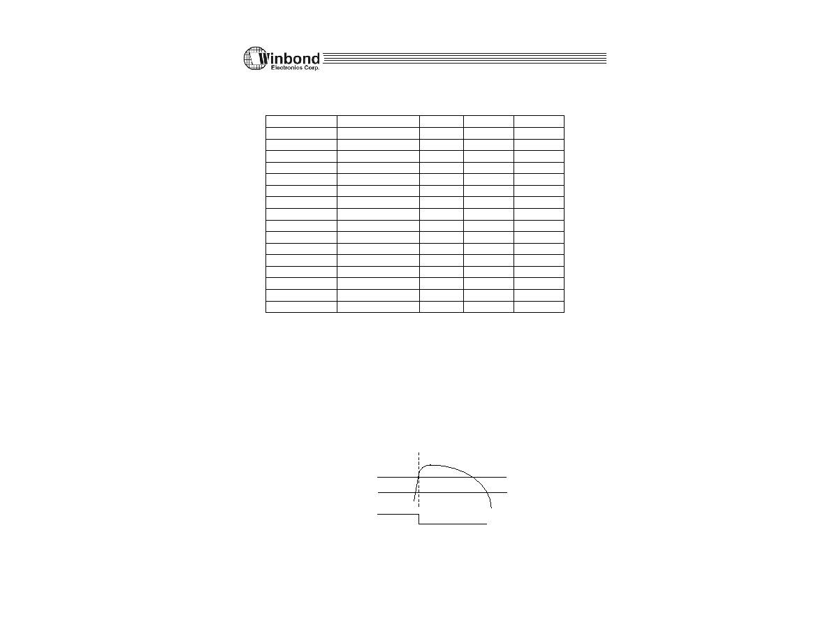
6.5 TEMP_FAULT#
The W83L785TS-S provides a good protection for temperature sensing. The W83L785TS-S
will issue an alert signal when the monitoring temperature exceeds the threshold. Setting pin 6
(TEMP_FAULT#) to monitor temperature and enable TEMP_FAULT# function. When
monitoring CPUT1 (Pin 2) temperature exceeds temperature fault limit (ex: 90
o
C) in CR26, or
CR27, pin6 TEMP_FAULT# will be asserted. As figure 5 shows.
Figure 5. TEMP_FAULT#
TEMP_FAULT Limit
TEMP_FAULT#
90 DEG
60 DEG
Publication Release Date: April 2002
Revision 0.5
10
W83L785TS-S
Preliminary
7. CONTENT OF DATA REGISTERS
7.1 Configuration Register
Index 40h
Power on default [7:0] = 0010,1101 b
Bit Name Read/Write
Description
7
INITIALIZATION Read/Write
A one restores power on default value to all
registers except the Serial Bus Address register.
This bit clears itself since the power on default is
zero.
6 Reserved
Read/Write Reserved
5 Reserved
Read/Write Reserved
4 SOFT_PWDN
Read/Write Software Power Down. If setting to 1,this chip
will power down, but I2C interface is still
working.
3 Reserved
Read/Write Reserved
2 En
_Temp
_FAULT
Read/Write
Enable Temperature Fault Function. When
Temperature 1 is out of the Temperature1 Fault
Limit value (defined in Index 85), the Pin 6 will
go to low level.
1
INT_ CLEAR
Read/Write
The device will stop monitoring. It will resume
upon clearing of this bit.
0
START
Read/Write
A one enables startup of monitored activities, a
zero puts the part in standby mode.
7.2 Reserved --Index 41h~4Bh
7.3 Winbond Vendor ID (Low Byte) - Index 4Ch (Auto Increase)
Power-on default [7:0] = 1010,0011 b (A3h)
Bit Name Read/Write
Description
7:0
VIDL[7:0]
Read Only
Vendor ID Low Byte. Default A3h.
7.4 Winbond Vendor ID (High Byte) - Index 4Dh (No Auto Increase)
Power-on default [7:0] = 0101,1100 b (5Ch)
Bit Name Read/Write
Description
7:0
VIDH[7:0]
Read Only
Vendor ID High Byte. Default 5Ch
Publication Release Date: April 2002
Revision 0.5
11
W83L785TS-S
Preliminary
7.5 Chip ID -- Index 4Eh
Power on default [7:0] = 0111,0000 b
Bit Name Read/Write
Description
7-0 CHIPID[7:0]
Read
Only Winbond Chip ID number. Read this register will
return 70h for W83L785TS.
7.6 Reserved -- Index 4Fh~51h
7.7 Thermal Sensor 1/2 Type Register -- Index 52h
Power on default [7:0] = 0000-0011 b
Bit Name Read/Write
Description
7-2 Reserved
Read/Write Reserved.
1-0 T1_TYPE[1:0]
Read/Write Temperature sensor 2 (environment) type.
0x - Thermistor (10K @ 25 C,
=3435)
o
11 - Thermal diode.
7.8 Temperature 1 Fault Limit -- Index 53h
Power on trapping
Bit Name Read/Write
Description
7-0 TEMP1_LM
Read/Write Temperature sensor 1 Limit Value.
R1
R2
FAULT_LIMIT
VREF
Use two resistors to divide an four section to
represent different temperature fault limit value and
offset limit value. The table is shown as following.
ADCVAL[7]: are represented as Fault Limit Value
Publication Release Date: April 2002
Revision 0.5
12
W83L785TS-S
Preliminary
7.9 Reserved --Index 54h~84h
7.10 Temperature 1 OFFSET Register-- Index 85h
Power on trapping
ADCVAL<7> == FAULT_LIMIT1; ADCVAL<6:4> == OFFSET1
FAULT_LIMIT
Offset Temperature
ADC Value
R1
R2
85
0
0000_xxxx X
10K
85 22
0001_xxxx
91K
9.1K
85 24
0010_xxxx
30K
5.6K
85 26
0011_xxxx
20K
5.6K
85 28
0100_xxxx
13K
5.1K
85 30
0101_xxxx
91K
4.7K
85 32
0110_xxxx
68K
4.7K
85 34
0111_xxxx
18K
16K
90 0
1000_xxxx
16K
18K
90 22
1001_xxxx
5.1K
7.5K
90 24
1010_xxxx
4.7K
9.1K
90 26
1011_xxxx
4.7K
12K
90 28
1100_xxxx
5.1K
18K
90 30
1101_xxxx
3K
16K
90 32
1
110_xxxx 9.1K
91K
90 34
1
111_xxxx 10K
X
8. VALUE RAM AND LIMIT VALUE
8.1 Value RAM
Index 20h- 3Fh
Index A7-A0
Description
20-26h
Reserved
27h
Temperature 1 reading
28-3Fh Reserved
Publication Release Date: April 2002
Revision 0.5
13
W83L785TS-S
Preliminary
9. SPECIFICATIONS
9.1 Absolute Maximum Ratings
PARAMETER RATING
UNIT
Power Supply Voltage
-0.5 to 7.0
V
Input Voltage
3.3 to 5.5
V
Operating Temperature
0 to +70
�
C
Storage Temperature
-55 to +150
�
C
Note: Exposure to conditions beyond those listed under Absolute Maximum Ratings may adversely affect the life and reliability of the device.
9.2 DC Characteristics
(Ta = 0
�
C to 70
�
C, V
DD
= 3.3~5V, V
SS
= 0V)
PARAMETER SYM
.
MIN
.
TYP. MAX. UNIT
CONDITIONS
I/O
12t
- TTL level bi-directional pin with source-sink capability of 12 mA
Input Low Voltage
VIL
0.8
V
Input High Voltage
VIH
2.0
V
Output Low Voltage
VOL
0.4
V
I
OL
= 12 mA
Output High Voltage
VOH
2.4
V
I
OH
= - 12 mA
Input High Leakage
ILIH
+10
�
A
VIN = VDD
Input Low Leakage
ILIL
-10
�
A
VIN = 0V
I/O
12ts
- TTL level bi-directional pin with source-sink capability of 12 mA and schmitt-trigger level input
Input Low Threshold Voltage
Vt-
0.5
0.8
1.1
V
VDD = 5 V
Input High Threshold Voltage
Vt+
1.6
2.0
2.4
V
VDD = 5 V
Hysteresis
VTH
0.5
1.2
V
VDD = 5 V
Output Low Voltage
VOL
0.4
V
I
OL
= 12 mA
Output High Voltage
VOH
2.4
V
I
OH
= - 12 mA
Input High Leakage
ILIH
+10
�
A
VIN = VDD
Input Low Leakage
ILIL
-10
�
A
VIN = 0V
Publication Release Date: April 2002
Revision 0.5
14
W83L785TS-S
Preliminary
9.2 DC Characteristics, continued
PARAMETER SY
M.
MIN. TYP. MAX. UNI
T
CONDITIONS
OUT
12t
- TTL level output pin with source-sink capability of 12 mA
Output Low Voltage
VOL
0.4
V
I
OL
= 12 mA
Output High Voltage
VOH
2.4
V
I
OH
= -12 mA
OD
8
- Open-drain output pin with sink capability of 8 mA
Output Low Voltage
VOL
0.4
V
I
OL
= 8 mA
OD
12
- Open-drain output pin with sink capability of 12 mA
Output Low Voltage
VOL
0.4
V
I
OL
= 12 mA
OD
48
- Open-drain output pin with sink capability of 48 mA
Output Low Voltage
VOL
0.4
V
I
OL
= 48 mA
IN
t
- TTL level input pin
Input Low Voltage
VIL
0.8
V
Input High Voltage
VIH
2.0
V
Input High Leakage
ILIH
+10
�
A
VIN = VDD
Input Low Leakage
ILIL
-10
�
A
VIN = 0 V
IN
ts
- TTL level Schmitt-triggered input pin
Input Low Threshold Voltage
Vt-
0.5
0.8
1.1
V
VCC = 5 V
Input High Threshold Voltage
Vt+
1.6
2.0
2.4
V
VCC = 5 V
Hysteresis
VTH
0.5
1.2
V
VCC = 5 V
Input High Leakage
ILIH
+10
�
A
VIN = VCC
Input Low Leakage
ILIL
-10
�
A
VIN = 0 V
Publication Release Date: April 2002
Revision 0.5
15
W83L785TS-S
Preliminary
9.3
AC Characteristics
VALID DATA
SCL
SDA IN
SDA OUT
t HD;SDA
t SCL
t HD;DAT
t SU;STO
t SU;DAT
Serial Bus Timing Diagram
Serial Bus Timing
PARAMETER SYMBOL
MIN.
MAX.
UNIT
SCL clock period
t
-
SCL
10
uS
Start condition hold time
t
HD;SDA
4.7
uS
Stop condition setup-up time
t
SU;STO
4.7
uS
DATA to SCL setup time
t
SU;DAT
120
nS
DATA to SCL hold time
t
HD;DAT
5 nS
SCL and SDA rise time
t
R
1.0
uS
SCL and SDA fall time
t
F
300
nS
Publication Release Date: April 2002
Revision 0.5
16
W83L785TS-S
Preliminary
10.
HOW TO READ THE TOP MARKING
The top marking of W83L785TS-S
W 83L78
5TS - S
212OA
Left: Winbond logo
1st line and 2nd line: Type number W83L785TS-S, S means SOP (Thickness = 150mil).
3rd line: Date code 212 O A
2 12: packages made in 2002, week 12
O: assembly house ID; A means ASE, O means OSE, G means Greatek
A: IC revision; A means version A, B means version B
Publication Release Date: April 2002
Revision 0.5
17
W83L785TS-S
Preliminary
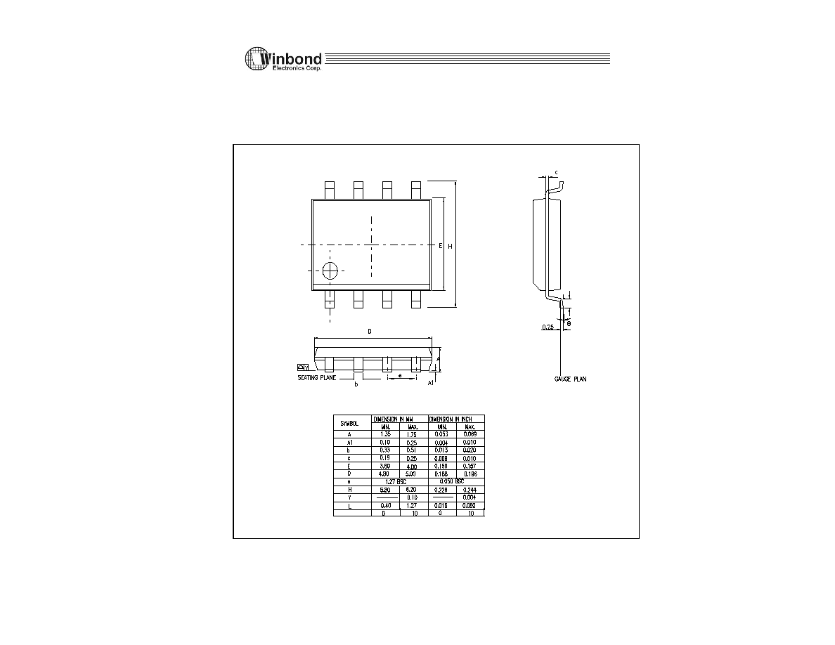
11. PACKAGE AND DIMENSIONS
E
1
8
5
4
Control demensions are in milmeters .
E
8L SOP-150mil
Publication Release Date: April 2002
Revision 0.5
18

W83L785TS-S
Preliminary
Publication Release Date: April 2002
Revision 0.5
19
Preliminary
Publication Release Date: April 2002
Revision 0.5
20
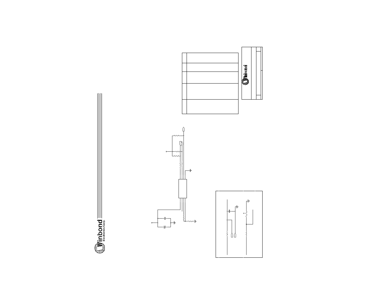
R1
30
Temp_fault
1101XXXX
22
30K
16K
68K
7.5K
24
TEMP_FAULT
1000XXXX
85
4.7K
5.1K
R8
15K 1%
0101XXXX
1111XXXX
Ver 0.4 W83L785TR_S change to W83L785TS_S
R3
4.7K
R4
4.7K
C3
3300P
Temp
90
T
RT1
THERMISTOR
10K 1%
0010XXXX
16K
D+
85
34
0
0001XXXX
VREF
20K
16K
1011XXXX
18K
34
0111XXXX
0
9.1K
0011XXXX
1110XXXX
R5
4.7K
85
10K
1100XXXX
4.7K
WINBOND ELECTRONICS CORP.
SDA
90
10K
1010XXXX
9.1K
9.1K
85
OFFSET
26
VCC
Temp
W83L785TS.SCH
0.4
W83L785TS_S Application Circuit
B
1
1
Wednesday, February 27, 2002
Title
Size
Document Number
Rev
Date:
Sheet
of
90
13K
5.6K
TEMPERATURE SENSORING CIRCUIT
24
R1
32
4.7K
12K
91K
VREF
R6
33
90
22
5.1K
I2C ADDRESS 0x5CH
U1
W83L785TS_S
1
2
3
4
5
6
7
8
VDD
CPUT
Vref
OFFSET/Fault_limit
GND
Temp_fault#
SDA
SCL
5.1K
85
26
{
1001XXXX
90
4.7K
C2
0.1u
28
R7
33
32
Temp
R9
10K 1%
OFFSET/FAULT_LIMIT
0110XXXX
18K
0000XXXX
91K
X
90
18K
C1
10u/16V
85
85
90
5.6K
SCL
30
VCC
3K
R2
Ver 0.3 pin6 Temp_fault# change to Temp_fault
0100XXXX
90
85
28
91K
VREF
R2
X
From
CPU
D-
W83L785TS-S