 | –≠–ª–µ–∫—Ç—Ä–æ–Ω–Ω—ã–π –∫–æ–º–ø–æ–Ω–µ–Ω—Ç: W89C940F | –°–∫–∞—á–∞—Ç—å:  PDF PDF  ZIP ZIP |

W89C940
ELANC-PCI (TWISTED-PAIR ETHER-LAN CONTROLLER WITH
PCI INTERFACE)
GENERAL DESCRIPTION
he ELANC-PCI (Twisted-pair Ether-LAN Controller with PCI Interface) integrates a W89C902 Serial(ELANC-
PCI) LAN Coprocessor for Twisted-Pair (SLCT) and PC/AT PCI bus interface logic into a single chip. The
ELANC-PCI provides an easy way of implementing the interface between an IEEE 802.3-compatible Ethernet
and a personal computer, ELANC-PCI also provide fast DMA operation to improve the packet transmit and
receive performance.
The PCI bus is a high performance local bus architecture with low latency random access time. It is a
synchronous bus with operation up to 33MHz. The PCI bus interface is designed to provide the registers with
the device information required for configuration, recording the status of the lines , control registers, interrupt
line and I/O base address registers. It is capable of functioning in a half-duplex environment.
The W89C940Fis designed to fully comply with the standard of PCI 2.0 specification. Taking advantage of PCI's
nature, W89C940F supports auto-configuration function to free users' depression and confusion on tunning
system resources conflict. With extremely high throughput on PCI bus, W89C940F offers a 32 bits data path to
highly boost its performance without extra cost. Comparing with LAN card with ISA bus, its improvement is
excellent. Besides, it also supports up to 256KB flash memory reserved for various applications, for instance
anti-virus, popular drivers, Boot ROM, viewing your PC assets...etc., and what is more, these software are able
to be updated on line. This can increase more niche feature on your LAN card, help you get more and bright
your company profile. W89C940F is a single chip - build-in PCI bus interface and all necessary circuits - which
will let design and board assembly become easy.
FEATURES
∑
Fully compatible with IEEE 802.3 standard
∑
Software compatible with Novell NE2000
∑
Complies with PCI Local Bus Specification Revision 2.0
∑
Slave Mode for PCI bus
∑
Fast DMA operation enhancing network access performance
∑
AUI, UTP interface available
∑
Supports one chip 32Kx8 and 16Kx8 SRAM
∑
Supports up to 64KB boot ROM
∑
EEPROM auto-load function after power on reset
∑
EEPROM on-board programming function available
∑
UTP interface polarity auto detection correction function available
∑
UTP/BNC auto media-switching function provided
∑
LED displaying for network segment Link/activity status
∑
Signature register available for device identification
∑
Single 5V power supply with low power consumption
∑
100 Pin PQFP

W89C940
2
PIN CONFIGURATION
50
5
1
5
2
5
3
5
4
5
5
5
6
5
7
5
8
5
9
6
0
6
1
6
2
6
3
6
4
6
5
6
6
6
7
6
8
6
9
7
0
7
1
7
2
7
3
7
4
81
7
5
7
6
7
7
7
8
7
9
8
0
82
83
84
85
86
87
88
89
49
48
47
46
45
44
43
42
41
40
39
38
37
36
35
34
90
91
92
93
94
95
96
97
98
99
100
1
2
3
4
5
6
1
0
1
1
7
8
9
1
2
1
3
1
4
1
5
1
6
1
7
1
8
1
9
2
0
2
1
2
2
2
3
2
4
2
5
2
6
2
7
2
8
2
9
3
0
33
32
31
V
C
C
A
D
2
2
A
D
2
1
A
D
2
0
A
D
1
9
A
D
1
8
A
D
1
7
A
D
1
6
A
D
1
5
C
B
E
#
2
/
F
R
A
M
#
E
I
R
D
Y
#
T
R
D
Y
#
D
E
V
S
E
L
#
S
T
O
P
#
G
N
D
V
C
C
P
A
R
C
#
B
E
#
1
A
D
1
4
A
D
1
3
A
D
1
2
A
D
1
1
A
D
1
0
A
D
9
A
D
8
C
/
B
E
#
0
B
U
S
C
L
K
G
N
D
V
C
C
D
N
G
P
X
T
N
X
T
N
X
R
P
D
C
P
X
R
N
D
C
A
C
T
E
E
C
S
B
P
C
S
B
R
C
S
B
M
S
A
1
4
\
L
M
S
A
1
3
M
S
A
1
2
M
S
A
1
1
M
S
A
M
M
1
0
S
A
M
S
A
M
S
A
M
S
A
M
S
A
M
S
A
M
S
A
M
S
A
M
S
A
S
A
9
8
7
6
5
4
3
2
1
0
V
C
C
X
1
X
2
G
N
D
TPDP
TPDM
XRDP
XRDM
DGND
RST#
INTA
AD31
AD30
AD29
AD28
AD27
AD26
AD25
AD24
AD23
C/BE3#
IDSEL
DGND
MSWRB
MSRDB
MSD7
MSD6
MSD5
MSD4
MSD3
MSD2
MSD1
MSD0
AD0
AD1
AD2
AD3
AD4
AD5
AD6
AD7
DGND
DVCC
W89C940(100 PINS)
#
AVCC
D
D
D
D
D
D
D
A
W89C940
3
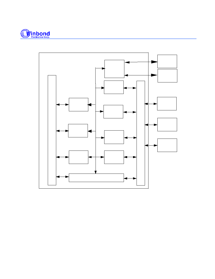
BLOCK DIAGRAM
H
O
S
T
B
U
S
Config.
Registers
Interrupt
Control
Logic
PCI and
Interface
Logic
Local Bus
Arbitrator
Buffer
Memory
Control
EEPROM
Control
Logic
Boot ROM
Control
Logic
B
U
S
SLCT
Module
Data Buffer
M
E
M
O
R
Y
SRAM
BTROM
EEPROM
AUI
TPI

W89C940
4
PIN DESCRIPTION
PCI INTERFACE
NAME
NUMBER
TYPE
DESCRIPTION
CLK
29
in
Clock:
Bus clock from PCI bus. All of the PCI signals, except RST#, are synchronized by
rising edge of clock.
The allowable operating frequency of CLK for W89C940 is from 25MHz to 33MHz.
RST#
87
in
Reset:
Asynchronous reset signal from PCI bus.
AD[31:00]
AD31-
AD24
AD23
AD22-
AD16
AD15-AD8
AD7-AD0
89 - 96
99
2 - 8
19 - 26
33 - 40
t/s
Address and Data:
Bidirection bus for PCI address and data signals transaction. AD[31:00] is a time
division bus. Two phases are used to carry the address and data messages of PCI
bus. The address phase is the clock cycle in which FRAME# is aeerted.
AD[31:24] contains the most significant byte(MSB) and the AD[7:0] contain the least
significant byte(LSB) during the data phase.
The data written from host should be stable and valid when IRDY# is asserted. The
data driven by W89C940 will be stable and valid when TRDY# is asserted.
C/BE[3:0]#
C/BE3#
C/BE2#
C/BE1#
C/BE0#
97
9
18
27
t/s
in
Bus Command and Byte Enables:
C/BE[3:0]# define the type of bus command during the address phase and the byte
enables during the data phase of a transaction. There are 16 types of bus
command defined in PCI bus. Four bits of C/BE[3:0]# are used to decode the 16
types of bus command. The byte enable determine which byte lanes carry
meaningful data.
C/BE0# indicate the byte 0(AD[7:0]) is valid. C/BE1# indicate the byte 1(AD[15:8]) is
valid. C/BE2# indicate the byte 2(AD[23:16]) is valid. C/BE3# indicate the byte
3(AD[32:24]) is valid.
PAR
17
t/s
Parity:
Even parity across AD[31:0] and C_BE[3:0]B.
W89C940 will drive the PAR in read data phase. The host drives the PAR for
address phase and writes data phase. PAR is stable and valid one clock after the
address phase. PAR is stable and valid one clock after either IRDY# is asserted on a
write transaction or TRDY# is asserted on a read transaction. Once PAR is valid, it
remains valid until one clock after the completion of the current data phase.
FRAME#
10
s/t/s
in
Cycle Frame:
FRAME# is asserted by host to indicate the beginning of a bus transaction. When
FRAME# is deasserted, the transaction is in the final data phase.

W89C940
5
PCI INTERFACE
NAME
NUMBER
TYPE
DESCRIPTION
IRDY#
11
s/t/s
in
Initiator Ready:
Initiator Ready indicates the host's ability to complete the current data phase of
transaction. During a write cycle, IRDY# indicates that valid data is presented on
AD[31:00]. During a read cycle, it indicates the master is ready to accept the
data. The wait cycles are inserted till IRDY# and TRDY# are asserted at the
same cycle.
TRDY#
12
s/t/s
Target Ready:
Target Ready indicates the W89C940's ability to complete the current data phase
of transaction. During a read cycle, TRDY# indicates that valid data is presented
on AD[31:00]. During a write cycle, it indicates the W89C940 is ready to accept
the data. The wait cycles are inserted till both IRDY# and TRDY# are asserted at
the same cycle.
STOP#
14
s/t/s
STOP:
Stop indicates W89C940 is requesting the master to stop the current transaction.
IDSEL
98
in
Initialization Device Select:
IDSEL is used as a chip select during PCI configuration read and write
transaction.
DEVSEL#
13
s/t/s
Device Select:
DEVSEL# will be asserted when W89C940 decode the correct address.
INTA#
88
o/d
Interrupt Request:
INTA# is used to request an interrupt service. The interrupt signal can be
masked by the register of IMR( Interrupt Mask Register). INTA# status is kept at
ISR( Interrupt Status Register).
NETWORK INTERFACE
NAME
NUMBER
TYPE
DESCRIPTION
X1
X2
53
52
I/TTL
O/TTL
Crystal or Oscillator Input.
Crystal or oscillator input (X1) and output (X2) pin. If a crystal is used, it should
be connected directly to X1 and X2. If an oscillator is selected, X1 is the 20 MHz
input and X2 should be left floating.
TXP
TXN
75
74
O/AUI
AUI Transmit Output:
AUI differential output pair. The data transmitted by DTE will be sent through TXP
and TXN in a differential signal with manchest code format. A 270 ohm pull-down
resistor is required for each of TXP and TXN. TXP and TXN should be isolated
by a pulse transformer from directly connecting outside loop.

W89C940
6
NETWORK INTERFACE
NAME
NUMBER
TYPE
DESCRIPTION
RXP
RXN
79
78
I/AUI
AUI Receive Input:
AUI differential input pair. The data received by network transceiver will be sent
back through RXP and RXN in a differential signal format. The RXP and RXN
are also should be isolated by a pulse transformer.
CDP
CDN
77
76
I/AUI
AUI Collision Input:
AUI differential input pair. The network transceiver will drive a 10MHz
differential signal onto CDP and CDN when a collision event is occurred. The
CDP and CDN should be isolated by a pulse transformer.
XRDP
XRDM
84
85
I/TPI
TPI Receive Input:
10BASE-T receive differential input pair. RXP and RXN should be shunted by
a 100 ohms resistor for twisted-pair line impedance matching.
TPDP
TPDM
82
83
O/TPI
TPI Transmit Output:
10BASE-T transmit differential output pair. A 1.21K ohm shunt resistor is
required across the TXP and TXN for signal pre-equalization.
ACT
73
O/LED
Activity Displaying:
Network activity displaying. ACT will indicate the network activity status by three
types of signals(DC 0 , DC1 and AC 10Hz).
DC 0 : indicating "Link Good", if UTP is selected.
DC 1 : indicating 1) "Link fail", if UTP is selected.
2) "idle", if AUI is selected.
AC 10HZ : indicating the DTE is transmitting a packet or the carrier on the
network is detected by the transceiver and the carrier sense signal is received
by W89C940.
The ACT will keep DC 1 if there is an abnormal network collision occurred, f.g.
the transceiver collision signal always active.
MEMORY INTERFACE
NAME
NUMBER
TYPE
DESCRIPTION
MSD[7:0]
48 - 41
B/MOS
Local Memory Data Bus:
A bidirection bus for data transfer between the local memory and the W89C940.
MSD0 is used as a serial data input pin during the auto configuration duration for
hardware reset. The data drove by the DO of EEPROM will clocked into the
MSD0 when the EEPROM load operation is active. The Ethernet node ID and
optional configuration content will be loaded into chip
`s
registers at this moment.
MSD1 is used as a serial data output pin during the auto configuration duration for
hardware reset.The command drove by the MSD1 will be clocked into the DI of
EEPROM for accessing the content of EEPROM.
MSD2 supplies the clock with a period of 1.2
µ
S for EEPROM during auto
configuration duration.

W89C940
7
MEMORY INTERFACE
NAME
NUMBER
TYPE
DESCRIPTION
MSRDB
49
O/MOS
Local Memory Read Enable.
An active low signal to enable the local SRAM read.
MSWRB
50
O/MOS
Local Memory Write Enable.
An active low signal to enable the local SRAM write.
MSA[14:0]
69 - 55
O/MOS
Local Memory Address Bus.
Address bus for local memory addressing.
The MSA14 will be used as the address strobe signal when the size is larger than
32Kx8. If the ROM size is larger than 32Kx8, Boot ROM address !13-A10 is
connected to MSA13-MSA10 and A17-A14 is connected to the latched MSA13-
MSA10. The valid address for the higher significant bits(A14,A15,....) will be stable
before the BPCSB is active low and should be latched by an external data latch
which is triggered by MSA14. The A0 ~ A13 of the BOOT ROM device are
connected to MSA0 ~ MSA13 directly no matter the BOOT ROM size is larger
than 32Kx8 or not.
RCSB
70
O/MOS
Memory Chip Select:
The RCSB is active low.
RCSB enables the local memory read/write cycle in conjunction with the MSRDB,
MSWRB pins.
BPCSB
71
O/MOS
BOOT ROM Chip Select:
BPCSB is active low.
BPCSB enables the BOOT ROM read cycle during the system booting up.
EECS
72
O/MOS
EEPROM Chip Select.
The EEPROM read/write operation will be enabled when EECS is active high.
POWER PINS
NAME
NUMBER
TYPE
DESCRIPTION
DVCC
1, 16, 30,
31, 54
I
Digital Power Supply:
5V DC power supply for internal digital logic circuitry.
DGND
15, 28, 32,
51, 86, 100
I
Digital Ground:
Ground pins for internal digital logic circuitry.
AVCC
81
I
Analog Power Supply:
5V DC power supply for internal analog circuitry.

W89C940
8
POWER PINS
NAME
NUMBER
TYPE
DESCRIPTION
AGND
80
I
Analog Ground:
Ground pin for internal analog circuitry.
It is recommended that there is a decoupling capacitor connected between the
power supply pins and ground pins. A RC low pass filter is also recommended to
be used for analog power supply.
Note: Signal Type Definition
in
Input is a standard input-only signal
out
Totem Pole output is a standard active driver.
t/s
Tri-State is a bi-directional, tri-state input/output pin.
s/t/s
Sustained Tri-State is an active low tri-state signal owned and driven by one and only one agent
at a time. The agent that drives an s/t/s pin low must drive it high for at least one clock before
letting it float. A new agent cannot start driving a s/t/s signal any sooner than one clock after the
previous owner tri-states it. A pull-up is required to sustain the inactive state until another agent
drives it, and must be provided by the central resource.
o/d
Open Drain allows multiple devices to share as a wire-OR.
W89C940
9
FUNCTIONAL DESCRIPTION
IEEE 802.3 MAC FUNCTION
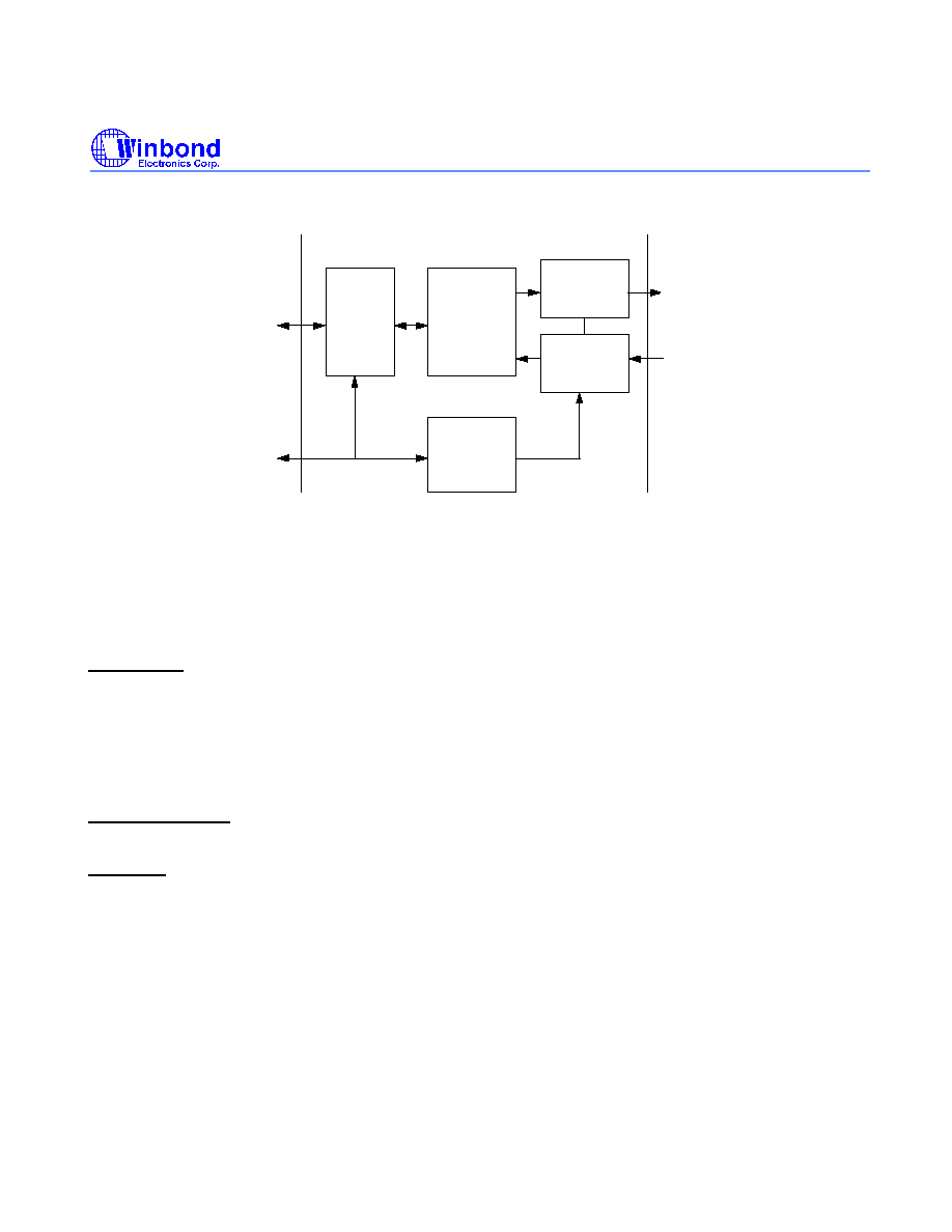
Core Coprocessor (SLCT) Operation
The SLCT core coprocessor has five major logic blocks that control Ethernet operations: the register files,
transmit logic, receive logic, FIFO logic, and DMA logic. The relationship between these blocks is depicted in
the following block diagram.
Register Files
The register files of the SLCT can be accessed in the same way as the configuration registers. The ELANC-PCI
should be in slave mode when the system accesses the register files. The command register (CR) determines
the page number of the register file, while the system address SA<0:3> selects one register address from 01H
to 0fH. The PCI IO read/write commands are used to activate the I/O operations. Refer to the W89C90 data
sheet for more detailed information on the registers.
DMA Interface Logic
The SLCT has two types of DMA operations, local DMA and remote DMA.
FIFO Logic
The SLCT has a 16-byte FIFO, which acts as an internal buffer to adjust transmission/reception speed
differences between DMAs. The FIFO has FIFO threshold pointers to determine the level at which it should
initiate a local DMA. The threshold levels are different for reception and transmission. The FIFO threshold
levels are defined in the DCR register.
The FIFO logic also provides a FIFO overrun and underrun signal for network management purposes. In a case
where the receive packets are flooding into the FIFO but the SLCT still does not have the bus authority, the
FIFO may be overrun. On the other hand, if a transmission begins before data are fed into the FIFO, it may be
underrun. Both cases result in a network error. These types of cases can be prevented by changing the values
of the FIFO thresholds.
PCI
Bus
Interface
DMA
Interface
Logic
16-byte
FIFO
Transmit
Logic
Receive
Logic
SNA
TX/RX
Logic
Register
Files
W89C940
10
Normally, the data in the FIFO cannot be read; reading FIFO data during normal operation may cause the
system to hang. In loopback mode, however, the SLCT allows FIFO data to be read by byte in order to check
the correctness of the loopback operation.
Receive Logic
The receive logic is responsible for receiving the serial network data and packing the data in byte/word
sequence. The receive logic thus has serial to parallel logic in addition to network detection capability.
The ELANC-PCI accepts both physical addresses and group addresses (multicast and broadcast addresses).
The SLCT extracts the address field from the serial input data. It then determines if the address is acceptable,
according to the configurations defined in the receive configuration register (RCR). If the address is not
acceptable, the packet reception is aborted. If the address is acceptable, the data packet is sent to the serial to
parallel logic before being fed into the FIFO. Data packets can thus be processed either byte or word-wide.
After receiving a data packet, the SLCT automatically adds four bytes of data receive status, next packet
pointer, and two bytes of receive byte count into the FIFO for network management purposes. The receive
status contains the status of the incoming packet, so that the system can determine if the packet is desired. The
next packet pointer points to the starting address of the next packet in the local receive ring. The receive byte
count is the length of the packet received by the SLCT. Note that the receive byte count may be different from
the "length" field specified in the Ethernet packet format. These four bytes of data will be transferred to the local
buffer with the last batch of the local DMA. However, these four bytes are stored at the first four addresses
before the packet.
Transmit Logic
The SLCT must be filled before transmission begins. That is, the local DMA read must begin before the SLCT
begins transmission. The SLCT first transmits 62 bits of preamble, then two bits of SFD, and then the data
packet. The parallel to serial logic serializes the data from the FIFO into a data packet. After the data packet,
the SLCT optionally adds four bytes of cyclic redundancy code (CRC) to the tail of the packet.
A protocol PLA determines the network operations of the ELANC-PCI. Collision detection, random backoff, and
auto retransmit are implemented in the transmit logic. The protocol PLA ensures that the ELANC-PCI follows
IEEE 802.3 protocol.
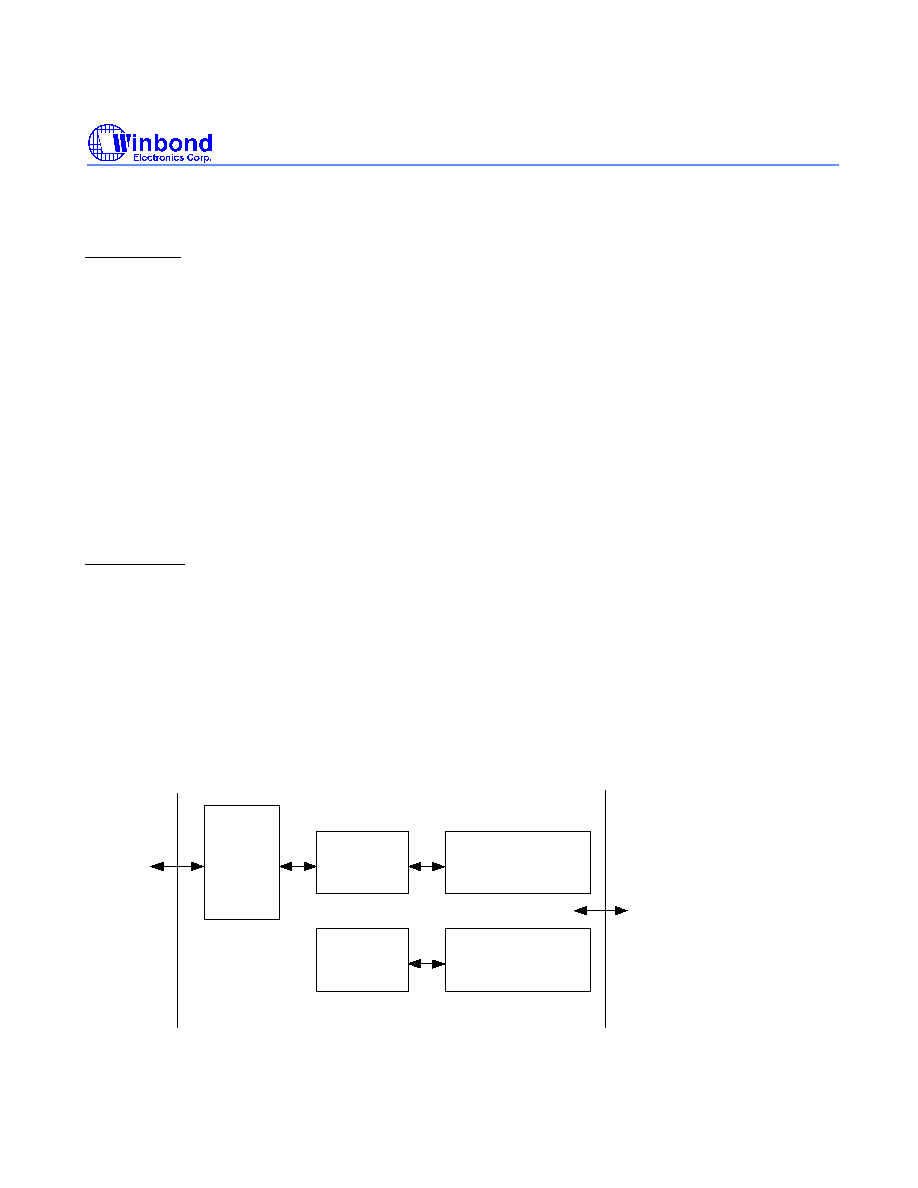
10BASE2 AND 10BASE5 PLS (PHYSICAL LAYER SIGNAL) FUNCTION
SNA Operation
TP
or
Coax
AUI
Interface
PLL
Manchester
Encoder/Decoder
osc/
crytal
SLCT Interface
Logic
L
C
E

W89C940
11
File 1
The ELANC-PCI also contains a Serial Network Adapter (SNA), which adapts the Non-Return-to-Zero (NRZ)
used in the core processor and host system to Manchester coded network symbols.
The SNA contains three blocks: a Phase Locked Loop (PLL), a Manchester encoder/decoder, and a collision
decoder, as well as crystal/oscillator logic.
The Manchester encoder/decoder handles code interpretation between NRZ signals and Manchester coded
signals. The PLL locks the receiving signals with an internal voltage control oscillator (VCO) so that network
noise(jitter) can be eliminated before the signals enter the core coprocessor. The collision decoder detects
whether the network is in a collision status.
10BASE-T MAU FUNCTION
TP Transceiver Operation
Transmit Driver
There are two signals for data transmission, TXP and TXN, which connect to the twisted-pair cable via a
transmitter filter and an optional common mode choke.
Smart Squelch
The main function of this block is to determine when valid data are present on the differential receiving inputs
(RXP/RXN). To ensure that impulse noise on the medium will not be taken as a valid datum, this circuit adopts
a combination of amplitude and timing measurements to determine the validity of the input signals. To qualify
incoming data, the smart squelch circuitry monitors the signals for three peaks of alternating polarity that occur
within a 400 nS window. Once this condition has been satisfied, the squelch level is reduced to minimize the
noise effect and the chances of causing premature Start Of Idle (SOI) pulse detection. If the receiver detects
activity on the receive line while packets are being transmitted, incoming data is qualified on five peaks of
alternating polarity so as to prevent false collisions caused by impulse noise. The squelch function returns to its
squelch state under any of the following conditions:
-
A normal Start Of Idle (SOI) signal
-
An inverted SOI signal
-
A missing SOI signal
A missing SOI signal is assumed when no transitions have occurred on the receiver for 175nS after a packet
has arrived. In this case, a normal SOI signal is generated and appended to the data.
Collision Detection
A collision occurs when transmit and receive signals occur simultaneously on the twisted pair cable. Collisions
will not be reported when the device is in link-fail state. The collision signal is also generated when the
transceiver has detected a jabber condition or when the SQE test is being performed.
SQE test
The Signal Quality Error (SQE) test is used to test the collision signaling circuitry in the Twisted Pair
Transceiver module. After each packet transmission, an SQE signal is sent to the SLCT. The SLCT expects this
signal and will flag an error if it does not exist.
Jabber
The jabber timer monitors the transmitter and disables the transmission if the transmitter is active for greater
than 26.2 mS.The jabber will re-enable the transmitter after the SLCT has been idle for at least 420 mS.

W89C940
12
Link Integrity
During periods of inactivity, link pulses are generated and received by both MAUs at either end of the twisted
pair to ensure that the cable has not been broken or shorted. A positive, 100 nS Link Integrity signal is
generated by the Twisted Pair Transceiver and transmitted on the twisted pair cable every 13 ms during periods
of no transmission activity. The ELANC-PCI assumes a link-good state if it senses valid link pulse activity on
the Twisted Pair Transceiver receive circuit. If neither receive data nor a link pulse (positive or negative) is
detected within 105 mS, the ELANC-PCI enters link-fail state. When a link-fail condition occurs, four
consecutive positive link pulses (or eight negative link pulses) must be received before a link-good condition is
assumed.
LCE CORE ACCESS FUNCTION
LCE core access function (LCE: Lan Controller of Ethernet)
The LCE core of the ELANC-PCI can be accessed by programming the register of the LCE core. The ELANC-
PCI's register files are mapped into the lower 16 I/O spaces: iobase to iobase+0FH. Any read/write to the
ELANC-PCI's registers is an "IN"/"OUT" command to these addresses.
Addresses iobase+10H to iobase+17H are mapped to the I/O port for the system to access the contents of the
buffer memory. Remote DMA reads and writes correspond to "IN"/"OUT" commands to these addresses.
When addresses iobase+18H to +1FH are read a software reset will be issued to the core coprocessor and
released about 780nsec later, automatically.
The following table summarizes the I/O address mapping:
ADDRESS
REGISTER
OPERATION
iobase+00H - iobase+0FH
LCE core's registers
Slave register read/write
iobase+10H - iobase+17H
I/O Ports
Remote DMA read/write
iobase+18H - iobase+1FH
Reset
Software reset
The buffer memory map for LCE core memory address space is summarized in the following table:
NE2000 COMPATIBLE
0000H - 001FH
ID Registers
0020H - 00FFH
0100H - 3FFFH
Unused
4000H - 7FFFH
16K X 8 local memory
8000H - FFFFH
Unused
NODE ID
Each node in an Ethernet network has a unique six-byte ID. The node ID is mapped into the memory space of
the ELANC-PCI. The ELANC-PCI will load the node ID from the EEPROM after power on reset. The node I.D.
should be allocated in the first 3 words(with the address of 00H ~ 02H) of the EEPROM.

W89C940
13
Bus Arbitration
The ELANC-PCI handles bus arbitration automatically. The LAN card can operate in four modes: idle state,
slave read/write mode, DMA mode, and PCI mode. The ELANC-PCI controls the on-board devices by decoding
these modes.
At power on, the ELANC-PCI is in idle mode. If a register read/write command is issued, the ELANC-PCI enters
the slave read/write mode. If a local DMA or remote DMA is initiated by the ELANC-PCI core coprocessor, the
ELANC-PCI enters DMA mode. A PCI command will put the ELANC-PCI into PCI mode. At any given time, the
ELANC-PCI can be in only one state. The ELANC-PCI handles state changes automatically. However, two
events, such as a DMA command and an PCI command, may be requested at the same time; in this case, the
ELANC-PCI allocates the bus on a first-come, first-served basis. No predefined priority is set within the
ELANC-PCI.
NE2000 MODE DMA FUNCTION
The ELANC-PCI provides two DMA channels for system access. The remote DMA mode moves data between
system memory space and local memory space. The local DMA moves data between the FIFO of the SLCT
and local memory space. However, since the SLCT can handle local DMA operations without system
intervention (refer to the data sheet for the SLCT), the system has to perform only remote DMA reads/writes.
In a transmit operation, the data should be moved to local memory before the system orders the SLCT to start
transmission. The remote DMA write moves the data from the PCI bus to the local SRAM. This is simply an
"OUT" command on the PC. For a receive operation, the network may feed data constantly and the local
memory may become full if the data are not moved out to system memory through a remote DMA read
operation. This operation is the "IN" command on the PC.
Remote DMA
A remote DMA can be performed only in I/O mode. The remote DMA moves data between the host and the
local buffers. Unlike a local DMA, the remote DMA is byte or word-wide. Each remote DMA operation transfers
four bytes, double-word, depending on the PCI cycle.
Since the remote DMA is simply an PCI I/O operation, PCI is sometimes affected by a remote DMA. If the
remote DMA is interleaved with other devices, TRDY# is deasserted to force the system to insert wait states.
The ELANC-PCI will automatically handle any arbitration necessary.
A Double word access on W89C940 from PCI bus is allowed. The buffer memory access will stop when the
Remote Byte Counter is decreased to zero. A double word read command will read only three bytes of valid
data if remote byte counter is set 3 or two bytes of valid data if the remote byte counter is set 2 respectively.
Local DMA
The local DMA transfers data from/to the on-board buffers. To perform data reception or transmission from/to
remote nodes in the network, data must be moved from/to the FIFO. To enhance the efficiency of the
transmission, the local DMA transfers data in batches: Data are first collected and then moved in a batch. Each
transfer can move up to 12 bytes of data at once. This scheme reduces time wasted in requesting the bus.
A local DMA begins by requesting the local bus. If the bus is available to the ELANC-PCI, it responds at once by
asserting the bus acknowledge; if, on the other hand, the bus is currently authorized to another device, the
ELANC-PCI will not assert the bus acknowledge and the SLCT must wait. Note that this sequence will not affect
the host system or the PCI bus signals. After each batch is transferred, the SLCT checks the FIFO threshold
levels to determine if another batch transfer should be requested.
W89C940
14
BOOT PROM ACCESS FUNCTION
Boot PROM Operation
For diskless applications, the system requires an on-board boot device. The ELANC-PCI allows the system to
use an on-board BOOT PROM as the boot device.
The BOOT PROM is essentially a byte-read device. ELANC-PCI will fetch a byte from the BOOT PROM and
drive the AD bus of the PCI Interface. If the system do a word read command, the ELANC-PCI will invoke two
byte read operation with consecutive address and drove the second byte on another byte of the PCI interface.
For double word command, the ELANC-PCI will deassert the TRDY# until four read operation with consecutive
address to the BOOT PROM is completed and then the four bytes of data will be drove onto the 32 bits data bus
of PCI.
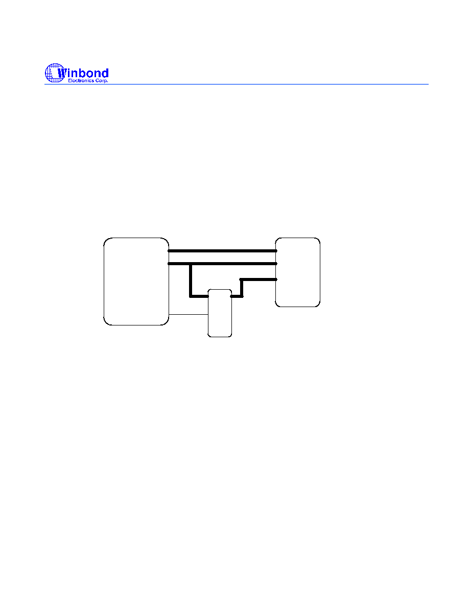
W89C940 can support the EPROM and Flash memory with 220nsec access time with the size up to 256KB. In
order to support 64KB,128KB and 256KB size with 15-bit address bus, W89C940 use MSA14 to latch the high
address bits MSA[17:14] from MSA[13:10]. The structure for address latch is shown as following.
W89C940
74LS373
EPROM
MSA14/L
MSA[9:0]
MSA[13:10]
MSA[17:14]

W89C940
15
CONFIGURATION PROGRAMMING FUNCTION
ELANC-PCI Mode Configuration Registers
MCR
A mode configuration register(MCR) is used to program the operation mode of the ELANC-PCI. The address is
page 0, 0AH. MCR can be updated by software. Reading this register is the same as reading a register in the
SLCT core coprocessor. Writing to these registers is done by first reading the register to be written to and then
using a slave write operation to update the configurations.
The content of MCR is as following table:
BIT
SYMBOL
DESCRIPTION
0
1
PHY0
PHY1
Physical Layer Interface:
These two bits select the type of physical interface which the ELANC-PCI
attached on. Both the thin Ehternet and thick Ethernet type use the AUI of
ELANC-PCI as the input/output interface. The other two UTP types,then, use
the TPI of ELANC-PCI as the input/output interface. The output and input pins
of AUI or TPI are idle, when the corresponding type is not selected.
PHY1 PHY0 Physical Interface Type
0 0 UTP (with 10BASE-T compatible receive squelch level)
0 1 Thin Ethernet
1 0 Thick Ethernet (AUI port)
1 1 UTP (with reduced receive squelch level)
2
GDLNK
Good Link Status:
A read operation on this bit will get the link test status. A "1" indicate that it is
link good and a "0" is link fail.
The GDLNK do not imply any information if the PHY0 and PHY1 is
programmed as Thin or Thick Ethernet.
3
LNKEN
Link Test Pulse enable:
The network media auto switching function, link integrity test function and the
link test pulse generation function will be enabled when LNKEN = "0".
Otherwise, all of these functions will be disabled when LNKEN = "1".
4
SHLS
SRAM High/Low Speed Select:
High speed SRAM with 20nsec access time is selected if SHLS =1. Low
speed SRAM with 70nsec access time is selected if SHLS =0.
5
6
7
BPS0
BPS1
BPS2
BOOT PROM Size:
The size of the BOOT PROM is selected by BPS0, BPS1, and BPS2.
BPS2 BPS1 BPS0 SIZE
0 0 X No boot PROM
0 1 0 8K
0 1 1 16K
1 0 0 32K
1 0 1 64K
1 1 0 128K
1 1 1 256K

W89C940
16
PCI Bus Operation Configuration Registers
The W89C940 implement a system configuration registers for PCI bus auto configuration function. The
W89C940 support the predefined header portion of the system configuration space ( i.e. first 64 bytes of the
256 bytes configuration space). A summarized table for those registers is as following.
address of
configuration
space
Register
Attribute
Default Value
after power ON
Write By
01H~00H
Vendor-ID
R/W
1050H
EEPROM
03H~02H
Device-ID
R/W
5A5AH
EEPROM
05H~04H
Command
R/W
0000H
System S/W
07H~06H
Status
R/W
0280H
System S/W
08H
Revision-ID
R/W
00H
EEPROM
0BH~09H
Class-Code
R
020000H
None
0CH
Cache-Line-Size
R
00H
None
0DH
Latency-Timer
R
00H
None
0EH
Header-Type
R
00H
None
0FH
BIST
R
00H
None
13H~10H
I/O-Base-Address
R/W
FFFFFFE1H
System S/W
17H~14H
Reserved-Reg.-0
R
00000000H
None
1BH~18H
Reserved-Reg.-1
R
00000000H
None
1FH~1CH
Reserved-Reg.-2
R
00000000H
None
23H~20H
Reserved-Reg.-3
R
00000000H
None
27H~24H
Reserved-Reg.-4
R
00000000H
None
2BH~28H
Reserved-Reg.-5
R
00000000H
None
2FH~2CH
Reserved-Reg.-6
R
00000000H
None
33H~30H
ROM-Base-Address
R/W
FFFF8001H
System S/W
37H~34H
Reserved-Reg.-7
R
00000000H
None
3BH~38H
Reserved-Reg.-8
R
00000000H
None
3CH
Interrupt Line
R/W
00H
System S/W
3DH
Interrupt Pin
R
01H
None
3EH
Min-Gnt
R/W
00H
EEPROM
3FH
Max-Lat
R/W
00H
EEPROM
The vendor ID, device ID, revision ID, Min-Gnt and Max-Lat are programmed by EEPROM, i.e. the contents of
these register can be updated by EEPROM load only. The I/O base address and the ROM base address
registers can be updated by system software. Those system configuration registers should be accessed by a
double word access operation. The W89C940 will drive 32 bits data on the bus when these configuration
registers are accessed.
Vendor ID Register
The vendor I.D. identifies the manufacturer of the device. Valid vendor identifiers are allocated by the PCI SIG
to ensure uniqueness. The content of this register will be updated after power on by the EEPROM load
operation. The vendor ID should be programmed into the word with 09H address of the EEPROM for power on
auto loading.

W89C940
17
Device I.D. Register
The device I.D. identifies the particular device. This identifier is allocated by the vendor.The content of this
register will be updated after power on by the EEPROM load operation. The device ID should be programmed
into the word with 0AH address of the EEPROM for power on auto loading.
Command Register
Bit Location
Attribute
Description
0
R/W
This bit controls the I/O space access response of W89C940. A
value of "0" will disables the W89C940 response. A value of "1"
allows the W89C940 to respond to I/O space accesses.
1
R/W
This bit controls the memory space access response of W89C940.
A value of "0" will disables the W89C940 response. A value of "1"
allows the W89C940 to respond to memory space accesses.
2
R
The W89C940 do not support PCI bus master function. This bit is
fixed to "0".
3
R
The W89C940 do not support the special cycle operation. This bit
is fixed to "0"
4
R
The W89C940 do not support the memory write cycle and the
invalidate command. This bit is fixed to "0".
5
R
The W89C940 is not a VGA compatible device. This bit is fixed to
"0".
6
R/W
This bit controls the parity error response of W89C940. A value of
"0" will force the W89C940 ignore a parity error. A value of "1"
allows the W89C940 to take a normal action when a parity error is
detected. This bit will be reset after power ON.
7
R
The W89C940 do not support data stepping function and this bit is
fixed to "0" always.
8
-
This bit is an enable bit for W89C940 internal SERR# driver. A
value of "0" will disables the internal SERR# driver. A value of "1"
enables the internal SERR# driver.
9~15
R
All of these bits are fixed to "0" internally. And no specific function
are related to these bits.

W89C940
18
Status Register
Bit Location
Attribute
Description
15
R/W
This bit will be set "1" by W89C940 when it detects a parity error,
even if parity error handling is disabled(as controlled by bit 6 in the
command register). A "write 1" operation on this bit will clear this
bit. This bit will be set "0" after it is cleared.
14
R/W
This bit will be set "1" by W89C940 when it assert the internal
SERR#. A "write 1" operation on this bit will clear this bit. This bit
will be set "0" after it is cleared. This bit is read only for 100 pin
package and is fixed to "0".
13
R
The W89C940 do not support PCI bus master function. This bit is
fixed to "0".
12
R
The W89C940 do not support PCI bus master function. This bit is
fixed to "0".
11
R/W
This bit will be set "1" by W89C940 when it terminates a
transaction with target-abort. A "write 1" operation on this bit will
clear this bit. This bit will be set "0" after it is cleared.
10~9
R
The Bit-10 is fixed to "0" and Bit-9 is fixed to "1". It indicated that
the W89C940 assert the DEVSEL# with medium speed.
8
R
The W89C940 do not support PCI bus master function. This bit is
fixed to "0".
7
R
The W89C940 support fast back-to-back transaction.
6~0
R
All of these bits are fixed to "0" internally. And no specific function
are related to these bits.
There are two cases that the W89C940 will initiate the target-abort. The first one is the addressing parity check
error cause internal SERR# asserted but without STOP# signal and the second one is the byte enable and
address check error that the STOP# is asserted. If addressing don't match the following table, the target doesn't
transfer the data, but terminate with target abort.
AD1
AD0
C/BE3#
C/BE2#
C/BE1#
C/BE0#
0
0
X
X
X
0
0
1
X
X
0
1
1
0
X
0
1
1
1
1
0
1
1
1
Revision I.D. Register
The revision I.D. is chosen by the vendor. It specifies a device specific revision identifier. Zero is an acceptable
value. It can be viewed as a vendor defined extension to the Device I.D. The content of this register will be
updated after power on by the EEPROM load operation. The revision ID should be programmed into the 23th
byte of the EEPROM for power on auto loading.
W89C940
19
Class Code Register
The Class Code Register is read only. The code of 020000H indicates that the W89C940 is a Ethernet
controller.
Cache-Line-Size Register
The W89C940 do not support the Memory Write and Invalidate command. All bits of this register are fixed to
"0".
Latency-Timer Register
The W89C940 do not implement a writable latency timer. All bits of this register are fixed to "0".
Header-Type Register
The W89C940 is a single function device. The bit 7 of header type register is fixed to "0" and all of other bits of
this register are also fixed to "0".
BIST Register
The W89C940 do not support the built in self test function. It will always return "00H" for a reading operation.
I/O-Base-Address Register
Bit
31~24
23~16
15~8
7
6
5
4
3
2
1
0
Attribute
R/W
R/W
R/W
R/W
R/W
R/W
R
R
R
R
R
Initial Value
FFH
FFH
FFH
1
1
1
0
0
0
0
1
The bit 0 fixed to "1" indicates that W89C940 requires the I/O space of the system as its buffer for data transfer.
The bit 0 to bit 4 implemented as a read only field imply that W89C940 need a I/O space with a range of 32
bytes. The power-up software can determine how munch address space the device required by writing a value
of all 1's to the register and then reading the value back. The W89C940 will return 0's in all don't care address
bits(bit 0 ~ bit 4), effectively specifying the address required, if the IDSEL and the configuration command are
recognized. The I/O base address will be decided by the bit 5 to bit 31 of the I/O base address register. The
system software should write the base address(32 bits address) onto this register. The bit 0 to bit 4 will be
ignored by W89C940. The bit 5 to bit 31 will be used as a reference value of the address decoder of the
W89C940.
There are nine types of command decoded by C/BE[0:3]# during the address phase of a transaction. These
nine types of command are as the following table.
C/BE[3:0]#
Command Type
0010
I/O Read
0011
I/O Write
0110
Memory Read
0111
Memory Write
1010
Configuration Read
1011
Configuration Write
1100
Memory Read Multiple, this command will be decoded as the Memory Read command
1110
Memory Read Line, this command will be decoded as the Memory Read command
1111
Memory Write and Invalidate, this command will be decoded as the Memory Write command
The last three commands are used in cache memory access. The application of W89C940 do not support this
command.
W89C940
20
ROM-Base-Address Register
Bit
31~24
23~16
15~8
7~0
Attribute
R/W
R/W
R/W
R/W
Initial Value
FFH
FFH
80H
01H
The W89C940 supports 8Kx8, 16Kx8, 32Kx8, 64Kx8, 128Kx8 and 256Kx8 ROM address decoding function.
For a 8Kx8 ROM application, the upper 19 bits of this register correspond to the upper 19 bits of the expansion
ROM base address. The lower 13 bits of this register correspond to the size of the expansion ROM. Those bits
correspond to the size of the expansion ROM are determined by MCR bit 5, bit 6 and bit 7 and can not be
writable by the system configuration write command. The device independent configuration software can only
determined the bits corresponding to the base address. The following table describe the relationship between
the addressing bus, sizing bits and the MCR bit 5/6/7.
MCR.7
MCR.6
MCR.5
Addressing Bits
Sizing Bits
ROM Size
0
0
X
None
None
No BOOT ROM
0
1
0
31~13
12~0
8Kx8
0
1
1
31~14
13~0
16Kx8
1
0
0
31~15
14~0
32Kx8
1
0
1
31~16
15~0
64Kx8
1
1
0
31~17
16~0
128Kx8
1
1
1
31~18
17~0
256Kx8
The device independent configuration software can only determined the addressing bits. The bit 0 of the ROM
base address register will be reset "0" by W89C940 if the MCR is set as "No BOOT ROM", i.e. BPS0=0,
BPS1=0 and BPS2=0. The bit 0 of the ROM base address register will be set "1" if the MCR is programmed as
there is an expansion ROM device add-on the LAN adapter. The initial value of FFFF8001H indicates that there
is a 32Kx8 expansion ROM device existing. The initial value is changed according to the BOOT ROM size
selection in the MCR (Mode Configuration Register).
Interrupt Line Register
This register is a readable and writable register. The POST software of system could write the routing
information into this register as it initializes and configures the system. The value in this register tells which
input of the system interrupt controllers the device's interrupt pin i connected to. Device drivers and operating
systems can use this information to determine priority and vector information. For x86 based PCs, the value in
this register correspond to IRQ numbers (0-15) of the standard dual 8259 configuration. The value 255 is
defined as meaning "unknown" or "no connection" to the interrupt controller. Values between 15 and 255 are
reserved.
Interrupt Pin Register
The W89C940 use the INTA# as its interrupt pin. The content of this register is fixed into "01".
Min-Gnt Register
It is used for specifying how long a burst period the device needs assuming a clock rate of 33MHz. The content
of this register will be updated after power on by the EEPROM load operation. The Min-Gnt should be
programmed into the 17th byte of the EEPROM for power on auto loading.

W89C940
21
Max-Lat Register
It is used for specifying how often the device needs to gain access to the PCI bus.
MAX_LAT is used to set the devices desired settings for Latency Timer values. The registers specify the values
in units of 0.25 microsecond. Zero means the device has no major requirements for the settings of Latency
Timer. The content of this register will be updated after power on by the EEPROM load operation. The Max-Lat
should be programmed into the 18th byte of the EEPROM for power on auto loading.
EEPROM PROGRAMMING FUNCTION
EEPROM Load and Reload procedure
A EEPROM control register(ECR) is used to control the operation mode of the EEPROM. The ECR is allocated
on the register address of page 3, 02H of LCE. The content of ECR is as following table:
BIT
SYMBOL
DESCRIPTION
0-5
Reserved
6
ERWS
EEPROM Read Write Select:
The write sequence to EEPROM is selected If ERWS = 1. If ERWS =
0, the read sequence is selected.
7
EAC
EEPROM Access Control:
EAC will enable the EEPROM read/write sequence if EAC = 1. The
EAS will be reset to " 0 " if the read/write sequence finished. Set EAC
= 0 will abort the EEPROM read/write sequence immediately.
The read/write sequence for EEPROM is described as following two statements.
Write Sequence:
write(ECR with ERWS=1 and EAC=1); /* enable the write sequence */
write(BFR, address); /* specify the address in which the data will be modified */
write(BFR, word_data); /* specify the data which will be write into the EEPROM */
repeat( read(ECR.EAC); ) until (EAC=0); /* wait for the programming process completed */
File2
Any operation that violate the write sequence will cause the EEPROM programming process aborted. The BFR
is a buffer register located at the register address of page3, 04H of LCE. With the EEPROM load back
sequence specified above, the contents at the specified address will be overwritten by the new data. One word
of data is modified by each write sequence. The allowable address in which the content will be modified is from
00H to 3fH.
Read Sequence:
write(ECR with ERWS=0 and EAC=1); /* enable the read sequence */
write(BFR, address); /* specify the address in which the data will be read out */
repeat( read(ECR.EAC); ) until (EAC=0); /* wait for the reading process completed */
read(BFR);
/* read word data */

W89C940
22
The read data will be kept in the BFR after the reading process is completed. The content of BFR will not
changed except that the other write or read sequence is started or a write(BFR, address) operation is executed.
i.e. the data of BFR can be read out any time afterwards.
EEPROM Content
The format of EEPROM contents is as followings:
ADDRESS
HIGH BYTE
LOW BYTE
Bit 15 ~ Bit 8
Bit 7 ~ Bit 0
0FH
Reserved
Reserved
0EH
Reserved
Reserved
0DH
Reserved
Reserved
0CH
Reserved
Reserved
0BH
MCR
Revision I.D.
0AH
Device I.D.(high byte)
Device I.D.(low byte)
09H
Vendor I.D.(high byte)
Vendor I.D.(low byte)
08H
MAX_LAT
MIN_GNT
07H
57H
57H
06H
Reserved
Reserved
05H
Reserved
Reserved
04H
Reserved
Reserved
03H
Reserved
Reserved
02H
Ethernet Address 5
Ethernet Address 4
01H
Ethernet Address 3
Ethernet Address 2
00H
Ethernet Address 1
Ethernet Address 0
The 5757H located at 07H address is used for NE2000 compatibility. The ELANC-PCI will load this parameter
into its internal register file for NE2000 software compatibility.
EEPROM Load Timing
A system reset should allow at least 1usec for the W89C940 to decode the action as a reset. After reset signal,
the device start to read the EEPROM after 1usec. The read clock is sent by the W89C940 to the EEPROM.
Normally the period of the clock is 1.2usec. It will take about 14.4usec to read the 12 bytes of data from
EEPROM.
The reset timing is as shown below.
W89C940
23
Since the ELANC-PCI reloads data into the configuration registers each time the system is reset, caution should
be taken in handling resets. A system reset should keep low at least 480ns for the ELANC-PCI to decode the
action as a reset. Any signal on the RESET pin shorter than this will be interpreted as noise and no response
will be taken by the ELANC-PCI.
After the reset signal is recognized, the ELANC-PCI to read configurations and ID contents from the EEPROM.
The read clock is sent by the ELANC-PCI to the EEPROM. Normally the period of the clock is 1.2
µ
S. The
ELANC-PCI will serially generate the EEPROM address so that the configuration and ID
After the reset signal is recognized, the ELANC-PCI to read configurations and ID contents from the EEPROM.
The read clock is sent by the ELANC-PCI to the EEPROM. Normally the period of the clock is 1.2
µ
S. The
ELANC-PCI will serially generate the EEPROM address so that the configuration and ID will be read into the
internal register file of W89C940.
NETWORK STATUS LED DISPLAY FUNCTION
Network Segment Status LED Display
Network activity displaying. ACT will indicate the network activity status by three types of signals (DC0 DC1
and AC 10Hz).
DC 0 : indicating "Link Good", if UTP is selected.
DC 1 : indicating 1) "Link fail", if UTP is selected.
2) "idle", if AUI is selected.
AC 10Hz : indicating the DTE is transmitting a packet or the carrier on the network is detected by the
transceiver and the carrier sense signal is received by W89C940.
The ACT will keep DC 1 if there is an abnormal network collision occurred, e.g. the transceiver collision signal
always active.
UTP OR COAXIAL AUTO-SELECTION FUNCTION
Auto Media-Switching
The ELANC-PCI provides a UTP/BNC auto media-switching function. The physical interface will jump from UTP
to BNC when the ELANC-PCI is configured as UTP, link checking is enabled, and the current UTP path is
broken. It will jump back immediately after the UTP path has been reconnected. When the physical interface is
configured as BNC or AUI, this auto media-switching function will be disabled.
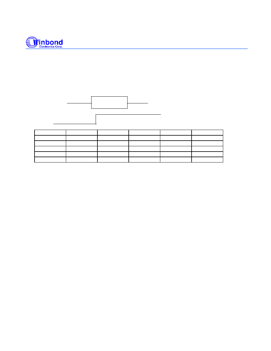
at least
EEREAD
RST#
1usec
1usec
14.4usec

W89C940
24
PHY1
PHY0
LNKEN
GDLNK
Auto Switching Function
0
0
1
1
disabled, keep at UTP
0
0
0
1
enabled, keep at UTP
0
0
0
0
enabled, UTP switch to BNC or AUI
0
1
1
1
disabled, keep at AUI
0
1
0
0 or 1
disabled, keep at AUI
1
0
1
1
disabled, keep at AUI
1
0
0
0 or 1
disabled, keep at AUI
1
1
1
1
disabled, keep at UTP
1
1
0
1
enabled, keep at UTP
1
1
0
0
enabled, UTP switch to BNC or AUI
SIGNATURE REGISTER
The signature register can be read by PCI Configuration Cycle with address 40H. The consecutive read will get
a data pattern 88H, 00H, 88H, 00H,.... if byte enable (C_BEB#) is asserted. A write operation will have no effect
on the content of this signature register.
Early Interrupt Function
1. Background:
W89C940 includes some control circuit and status register bits to generate interrupt signal early during
receiving packets. Besides traditional interrupt generated at incoming packet end, W89C940 can generate
interrupt when received packet bytes reach
"
Early Interrupt Threshold
"
and early interrupt function is enabled.
2. Register List:
Registers
IO Address
Descriptions
EIR_EN
Page 0
Base+0bh
[0]
Early Interrupt Enable Register: Read/Write
Asserted high to enable Early Interrupt Function. Deasserted to
disable Early Interrupt Function. To program Receive Control
Register (RCR) to monitor mode or Data Configuration Register
(DCR) to Loopback mode will also disable Early Interrupt
Function. Initial value after Power-on Reset is 0. Read once
write.
EIR_MASK
Page 0
Base+0bh
[1]
Early Interrupt Mask Register: Read/Write
Asserted high to initiate an interrupt on INTA# of PCI local bus
when an Early Interrupt Event occured. Deasserted this register
will mask an interrupt generated. Deasserted this register does
not disable Early Interrupt Status Register. Initial value after
Power-on Reset is 0.Read once write.
EIR_STATU
S
Page 0
Base+0bh
[7]
Early Interrupt Status Register: Read/Write
Asserted high when the byte count of incoming frame reaches
Early Interrupt Threshold with correct destination address (DS), in
the enable mode of Early Interrupt Function. Write 1 to clear
EIR_STATUS. Initial value after Power-on Reset is 0. Read
once write.

W89C940
25
EIR_THD
[15:0]
Page 3
Base+06h
[15:0]
Early Interrupt Threshold Register: Word Read/Write
Early Interrupt Threshold is in the unit of byte. The minimum
value of threshold is 64 bytes. Any value less than 64 bytes will
be treated as 64 bytes except value 0000h. Not to program
threshold or program 0000h will be disable Early Interrupt
function. The initial threshold value after Power-on Reset is
0000h.
CLDA0[7:0]
CLDA1[7:0]
Page 0
Base+01h[7:0]
Base+02h[7:0]
Current Local DMA Address Register: Read only.
Currrent Address of Local DMA. Use word IO read command to
access the content. Initial value after Power-on Reset is 0000h.
Using word command to read port base+01h will have both
CLDA0 & CLDA1.
3. Program Procedure:
a. Set EIR_EN=1 to enable Eraly Interrupt Function and set EIR_MASK=1 to enable interrupt pin
INTA# of PCI local bus.
b. Program eraly interrupt threshold, EIR_THD.
c. Set DCR not in Loopback mode.
d. Set RCR not in monitor mode.
e. Program CR to start receive packet.
f. Wait until a frame with a correct destination address and receive byte count greater than Early
interrupt Threshold.
g. An intrrupt initiated and EIR_STATUS register set.
ps: a, b, c, d & e can also be programmed individually.
PCI BUS TRANSACTION
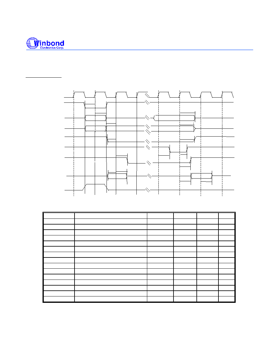
This section will introduce the Read Transaction, Write Transaction, and Termination Transaction of PCI bus.
Read Transaction ( I/O and Memory Read )
The timing of read transaction is shown in figure.
W89C940
26
CLK
1
2
3
4
5
6
7
8
AD[31::0]
ADDRESS
BUS CMD
DATA
BE#'s
PAR
STOP#
DEVSEL#
TRDY#
IRDY#
C_BE[3:0]#
FRAME#
The transaction is initiated by FRAME# , the address is asserted and bus read command of C/BE[3:0]# is also
asserted. This phase is called address phase. IRDY# (Initiator Ready) is asserted by master after address
phase. Target initiate TRDY#( Target Ready) and assert valid data on the bus. The DEVSEL# means the target
is addressed and respond to the master device. The data transaction is happened on both IRDY# and TRDY#
are asserted on the same clock edge that is called data phase. During the data phase, the BE (Byte Enable)
indicate the data length of the data. If it is a double word, 32 bits, the BE will be 0000. If data is a word, the BE
will be 1100 or 0011
If the host send the memory read command in burst mode, W89C940 accept the first data phase
access and then reject the further data access request with retry disconnection. Only one data phase
is allowed for transaction.
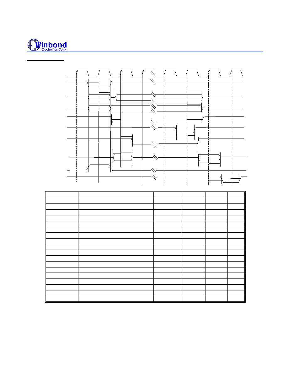
Write Transaction ( I/O and Memory Write)
The write transaction is like read transaction, the FRAME# initiate the transaction with address phase and the
data is written in data phase. The data could be asserted directly after address phase. It does not need a WAIT
state for avoiding bus contention. The transaction is ended when the FRAME#, IRDY#, TRDY# and DEVSEL#
are deasserted. If the host send the memory read command in burst mode, W89C940 accept the first data
phase access and then reject the further data access request with Retry disconnection. Only one data phase is
allowed for transaction.
The write transaction is as shown in the figure
W89C940
27
CLK
AD[31::0]
ADDRESS
BUS CMD
DATA
BE#'s
1
2
3
4
5
6
7
8
FRAME#
C_BE[3:0]#
IRDY#
TRDY#
DEVSEL#
STOP#
PAR
Configuration Read Transaction
The Configuration Read timing is as shown
CLK
AD[31::0]
ADDRESS
BUS CMD
DATA
BE#'s
1
2
3
4
5
6
7
IDSEL
8
FRAME#
C_BE[3:0]#
IRDY#
TRDY#
DEVSEL#
STOP#
PAR
The timing is the same as the figure I/O Read Transaction, except the IDSEL is asserted during the address
phase. The transaction access the configuration registers of the device.
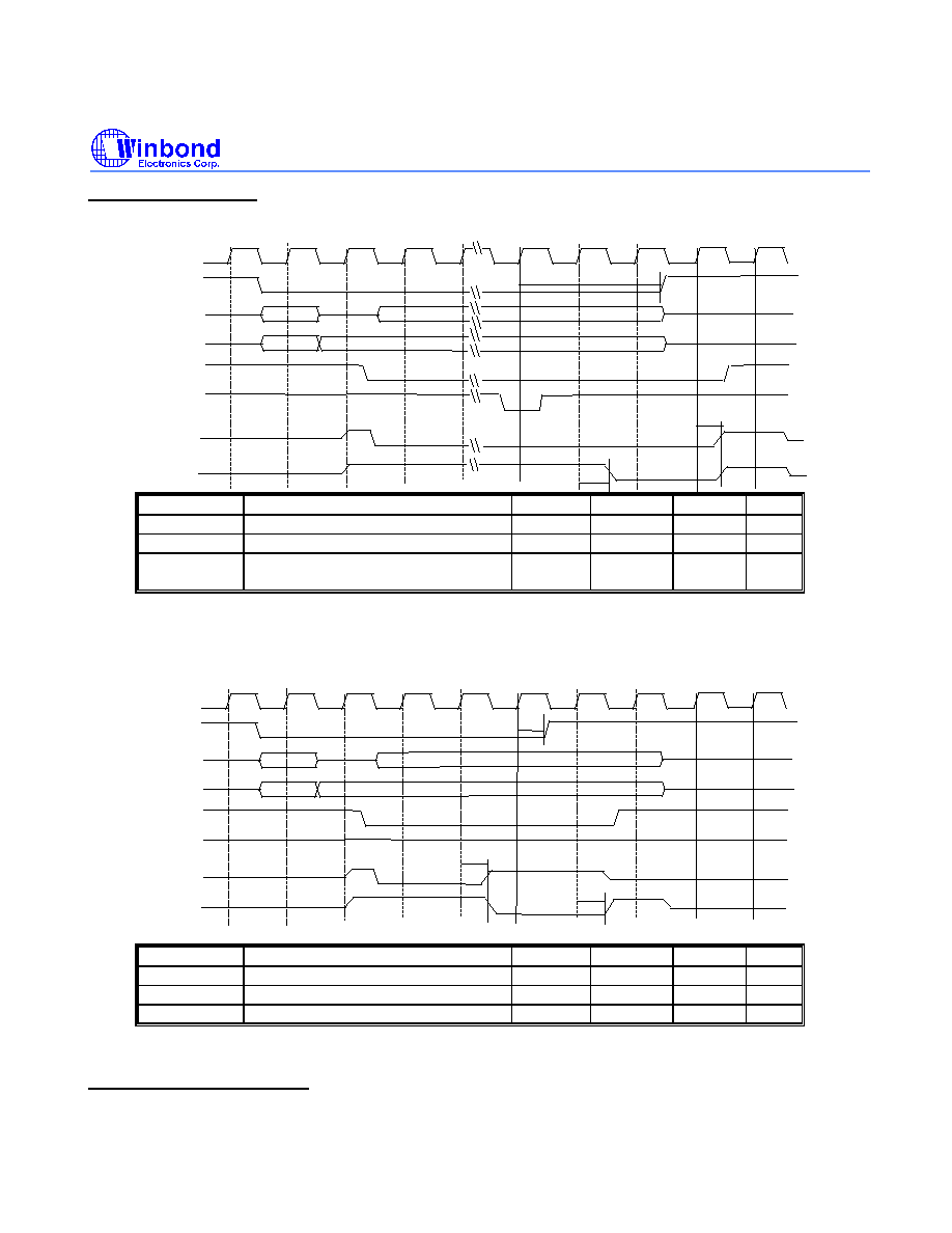
Configuration Write Transaction
The timing is as shown.
W89C940
28
CLK
AD[31::0]
ADDRESS
BUS CMD
DATA
BE#'s
1
2
3
4
5
6
7
8
FRAME#
C_BE[3:0]#
IRDY#
TRDY#
DEVSEL#
STOP#
PAR
IDSEL
The timing is the same as the figure I/O Read Transaction, except the IDSEL is asserted during the address
phase. The transaction access the configuration registers of the device.
Transaction Termination
Target Initiated Termination
The W89C940 device can only work in slave mode. It respond to the request from the master device and act as
a target. Sometimes the target are unable to answer the master device and initiate a termination. There are two
types of termination will occur. The first one is disconnect-C/Retry type. The second one is Target Abort type.
The timing is as shown in the figure
The first type is the Disconnect-C/Retry type, as shown in the figure
W89C940
29
CLK
FRAME#
AD[31::0]
IRDY#
TRDY#
ADDRESS
BUS CMD
BE#'s
1
2
3
4
15
16
17
C/BE[3::0]#
0
18
19
STOP#
DEVSEL#
Because W89C940 don't support memory command in burst mode. When the host try to send memory
command in burst mode, the first data phase is completed. TRDY# and IRDY# are deasserted, but the FRAME#
is asserted for the next data phase. The device will assert STOP# to terminate the transaction. Data is not
transferred after STOP# is asserted. The host need to initiate another transaction for further data transfer. The
timing is shown above.
The Target-Abort type, as shown in the figure
CLK
FRAME#
AD[31::0]
IRDY#
TRDY#
ADDRESS
BUS CMD
BE#'s
1
2
3
4
5
6
7
C/BE[3::0]#
0
STOP#
DEVSEL#
8
9
The condition is the target requires the transaction to be terminated and does not want the transaction tried
again. As shown in the figure, the DEVSEL# is deasserted when STOP# is asserted. If there is a data needed to
be transferred, DEVSEL# must be asserted for one or more clock cycles and TRDY# must be deasserted before
target-abort can be signaled.
There are two cases that the device will initiate the target-abort. The first one is the addressing parity check
error cause internal SERR# asserted and the second one is the Byte Enable and addressing check error. If
addressing don't match the following table, the target doesn't transfer the data, but terminate with target abort.
AD1
AD0
C/BE3#
C/BE2#
C/BE1#
C/BE0#
0
0
X
X
X
0
0
1
X
X
0
1
1
0
X
0
1
1

W89C940
30
1
1
0
1
1
1
W89C940
31
Fast Back-to-Back Transactions
CLK
FRAME#
AD[31::0]
IRDY#
TRDY#
DEVSEL#
STOP#
ADDRESS
BUS CMD
DATA
BE#'s
1
2
3
4
5
6
7
PAR
C/BE[3::0]#
8
ADDRESS
BUS CMD
BE#'s
DATA
Without contention of TRDY#, DEVSEL#, or STOP#, the IDLE states between transactions are removed. It
increase the throughput of the data transaction. If the first transaction is a write cycle and the second transaction
access( can be read or write transaction) to the same target , one IDLE cycle can be removed between
transactions.
Parity
As shown in the figure below, parity is generated at immediately following clock and the internal PERR# is after
PAR. Parity is calculated the same on all PCI transactions regardless of the type or form. Parity covers
AD[31:0] and C/BEB[3:0]# lines regardless of whether or not all lines carry meaningful information. The number
of 1s on AD[31:0], C/BEB[3:0]# and PAR equals an even number. Parity is also calculated at Configuration
phase.
CLK
FRAME#
AD[31::0]
ADDRESS
BUS CMD
DATA
BE#'s
1
2
3
4
5
PAR
PERR#
C_BE#[3::0]
W89C940
32
TEST MODE SETTING AND DEFINITION
W89C940 provide three test modes they are 90 test mode, TP test mode, and AUI test mode. The system reset
signal is fed into 400ns low glitch eater and the output is RST_I. At 400 nsec RST_I asserted period, the three
pins (EECS,BPCSB,RCSB) output (0,1,1). After RST_I deasserted, the three pins become input pins and
sample at 90nsec. The sampled value (*1,*2,*3) determine the test mode. The timing and test mode type is
shown as following.
400ns low
glitch eater
400ns low
glitch eater
PCI RSTB
RST_I
RST_I
EECS_O
0
Z
Z
Z
0
BPCS_O
1
Z
Z
Z
1
RCSB_O
1
Z
Z
Z
1
EECS_I
Z
Z
*1
Z
Z
BPCSB_I
Z
z
*2
Z
Z
RCSB_I
Z
z
*3
z
Z
EECS_O: EECS pin output driver
EECS_I : EECS pin input forcing
(*1, *2, *3)
= (0,1,1) ---- normal operation mode
= (1,0,0) ---- fast EEPROM mode
= (1,0,1) ---- 90 test mode
= (1,1,0) ---- TP test mode
= (1,1,1) ---- AUI test mode
= (0,0,0) ---- AUI linear mode
FILE 3

W89C940
33
ABSOLUTE MAXIMUM RATINGS
SYMBOL
PARAMETER
MINIMUM
MAXIMUM
UNIT
TA
Operating Temperature
0
70
∞
C
TS
Storage Temperature
-55
150
∞
C
V
DD
Supply Voltage
-0.5
7.0
V
V
IN
Input Voltage
V
SS
-0.5
V
DD
+0.5
V
V
OUT
Output Voltage
V
SS
-0.5
V
DD
+0.5
V
TL
Lead Temperature
(Soldering 10 seconds
maximum)
250
∞
C
POWER SUPPLY (VDD=4.75 V TO 5.25V, VSS=0 V, TA=0
∞
C TO 70
∞
C)
SYMBOL
PARAMETER
CONDITION
MINIMUM
MAXIMUM
UNIT
IDDI
Power Supply Current(idle, clock
active)
Vdd=5.25V
150
mA
IDDT
Power Supply Current(transmitting)
Vdd=5.25V
250
mA
DC CHARACTERISTICS (VDD=4.75 V TO 5.25 V, VSS=0 V, TA=0
∞
C TO 70
∞
C)
DIGITAL:
SYMBOL
PARAMETER
CONDITION
MINIMUM
MAXIMUM
UNIT
V
IL
Low Level Input Voltage
V
SS
-0.5
0.8
V
V
IH
High Level Input Voltage
2.0
V
DD
+0.5
V
V
OL
Low Output Voltage
IoL=4.0mA
0.4
V
V
OH
High Output Voltage
Ioh=-4.0mA
2.4
V
I
IL1
Input Leakage Current (Note 1)
Vin=5.25V
Vin=0V
10
µ
A
I
IL2
Input Leakage Current (Note 2)
Vin=5.25V
Vin=0V
2
mA

W89C940
34
I
OL
Tristate leakage Current
Vout=Vdd
Vout=Vss
-10
0.3
mA
µ
A
Note 1: All of the input pins except those stated in Note 2.; Note 2: XRDP, XRDM, CDP, CDN, RXP, RXN.
AUI:
SYMBOL
PARAMETER
CONDITION
MINIMUM
MAXIMUM
UNIT
V
DD
Differential Output Voltage (TXP/N)
as the test load
+/-550
+/-1200
mV
V
OB
Differential Idle Output Voltage
Imbalance (TXP/N)
as the test load
+/-40
mV
V
U
Undershoot Voltage (TXP/N)
as the test load
100
mV
V
DS
Differential Squelch Threshold
(CDP/N, RXP/N)
-175
-300
mV
V
CM
Differential Input Common Mode
Voltage (CDP/N, RXP/N)
2.0
4.0
V
TWISTED PAIR:
SYMBOL
PARAMETER
CONDITION
MINIMUM
MAXIMUM
UNIT
R
TI
XRDP/M Differential Input
Resistance
3
Kohms
V
TIB
XRDP/M Open Circuit Input
Voltage (bias)
-2.75
VDD-1.0
V
V
TIV
XRDP/M Differential Input Voltage
Range
VDD=5V
-3.1
3.1
V
V
TPS
XRDP/M Positive Squelch
Threshold
300
585
mV
V
TNS
XRDP/M Negative Squelch
Threshold
-585
-300
mV
V
TPU
XRDP/M Positive Unsquelch
Threshold
200
350
mV
V
TNU
XRDP/M Negative Unsquelch
Threshold
-350
-200
mV
V
TOH
TPDP/M High Output Voltage
I=32mA
VDDTP-.44
VDDTP
V

W89C940
35
V
TOL
TPDP/M Low Output Voltage
I=32mA
VSSTP
VSSTP+.44
V
I
TO
TPDP/M Output Current
32
mA
R
TO
TPDP/M Output Resistance
13.5
Kohms
W89C940
36
PRELIMINARY SWITCHING CHARACTERISTICS
PCI Accesses
Read Transaction
CLK
AD[31::0]
ADDRESS
DATA
BE#'s
1
2
3
BUS CMD
DEVSEL#
TRDY#
IRDY#
C/BE[3:0]#
FRAME#
T9
T11
T12
T13
T10
PAR
T7
INPUT
OUTPUT
T2
T3
T5
T8
T1
T4
T6
T14
T15
IDSEL#
0
SYMBOL
DESCRIPTION
MIN
TYPICAL
MAX
UNIT
T1
PCI input signal set up time*
7
nsec
T2
PCI input signal hold time*
0
nsec
T3
BE Byte Enable set up time
7
nsec
T4
BE Byte Enable hold time
0
nsec
T5
IRDY# set up time
7
nsec
T6
IRDY# hold time
0
nsec
T7
PAR input setup time
7
nsec
T8
PAR input hold time
0
nsec
T9
DEVSEL# driven time
11
12
13
nsec
T10
DEVSEL# hold time
11
12
13
nsec
T11
output data hold time
18
19
20
nsec
T12
TRDY# driven time
11
12
13
nsec
T13
TRDY# hold time
11
12
13
nsec
T14
PAR output driven time
11
12
13
nsec
T15
PAR output hold time
11
12
13
nsec
*address, command, and FRAME# for slave access, IDSEL# for configuration read transaction
W89C940
37
Write Transaction
CLK
AD[31::0]
ADDRESS
DATA
BE#'s
1
2
3
BUS CMD
DEVSEL#
TRDY#
IRDY#
C/BE[3:0]#
FRAME#
T9
T11
T12
T13
T14
T10
PAR
T7
INPUT
INPUT
T1
T2
T3
T5
T8
T15
T4
T6
T16
IDSEL#
PERR#
T17
T18
0
DATA
SYMBOL
DESCRIPTION
MIN
TYPICAL
MAX
UNIT
T1
PCI input signal setup time*
7
nsec
T2
PCI input signal hold time*
0
nsec
T3
BE Byte Enable set up time
7
nsec
T4
BE Byte Enable hold time
0
nsec
T5
IRDY# set up time
7
nsec
T6
IRDY# hold time
0
nsec
T7
PAR input setup time
7
nsec
T8
PAR input hold time
0
nsec
T9
DEVSEL# driven time
11
12
13
nsec
T10
DEVSEL# hold time
11
12
13
nsec
T11
input data set up time
7
nsec
T12
input data hold time
0
nsec
T13
TRDY# driven time
11
12
13
nsec
T14
TRDY# hold time
11
12
13
nsec
T15
PAR input setup time
7
nsec
T16
PAR input hold time
0
nsec
T17
Internal PERR# driven time**
11
12
13
nsec
T18
Internal PERR# hold time**
11
12
13
nsec
*address, command, and FRAME# for slave access, IDSEL# for configuration read transaction
**Internal PERR# will be asserted if the parity error event occurred.
W89C940
38
Transaction Termination
Disconnect-C/Retry Type
CLK
FRAME#
AD[31::0]
IRDY#
TRDY#
ADDRESS
BUS CMD
BE#'s
1
2
3
4
15
16
17
C/BE[3::0]#
0
T1
18
19
T3
STOP#
DEVSEL#
T2
SYMBOL
DESCRIPTION
MIN
TYP
MAX
UNIT
T1
FRAME# deasserted from clock 15
0
nsec
T2
Clock 16 to STOP# asserted time
11
12
13
nsec
T3
Clock 18 to STOP# and DEVSEL#
hold time
11
12
13
nsec
Note: 1) The other timing requirements for PCI input signal are as the read transaction timing.
2) T1,T2 and T3 are used for the disconnect type C(host try to transfer more than one data
phase).
Target-Abort Type
CLK
FRAME#
AD[31::0]
IRDY#
TRDY#
ADDRESS
BUS CMD
BE#'s
1
2
3
4
5
6
7
C/BE[3::0]#
0
T1
T2
STOP#
T3
DEVSEL#
8
9
SYMBOL
DESCRIPTION
MIN
TYP
MAX
UNIT
T1
FRAME# deasserted from clock 15
0
nsec
T2
Clock 4 to DEVSEL# hold time
11
12
13
nsec
T3
Clock 6 to STOP# hold time
11
12
13
nsec
Note: 1) The other timing requirements for PCI input signal are as the read transaction timing..
2) T2 and T3 are used for the target abort type(host addressing error).
Fast Back-to-Back Transactions
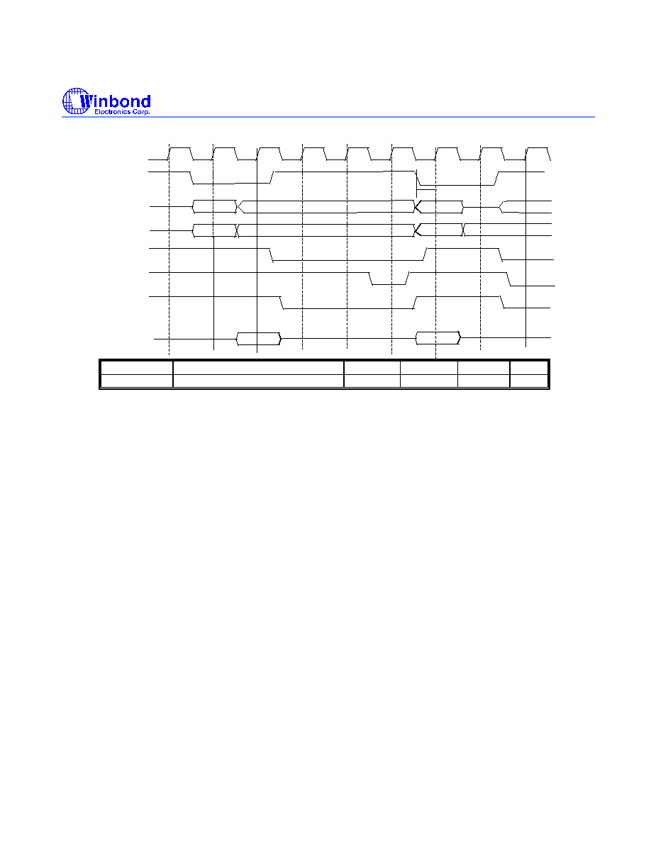
W89C940
39
CLK
AD[31::0]
DEVSEL#
TRDY#
IRDY#
C/BE[3:0]#
FRAME#
PAR
BUS CMD
BE#'s
ADDRESS
DATA
ADDRESS
WRITE DATA
BE#'s
1
2
3
4
5
6
7
8
BUS CMD
INPUT
INPUT
0
T1
SYMBOL
DESCRIPTION
MIN
TYPICAL
MAX
UNIT
T1
FRAME# set up time to clock 6
7
nsec
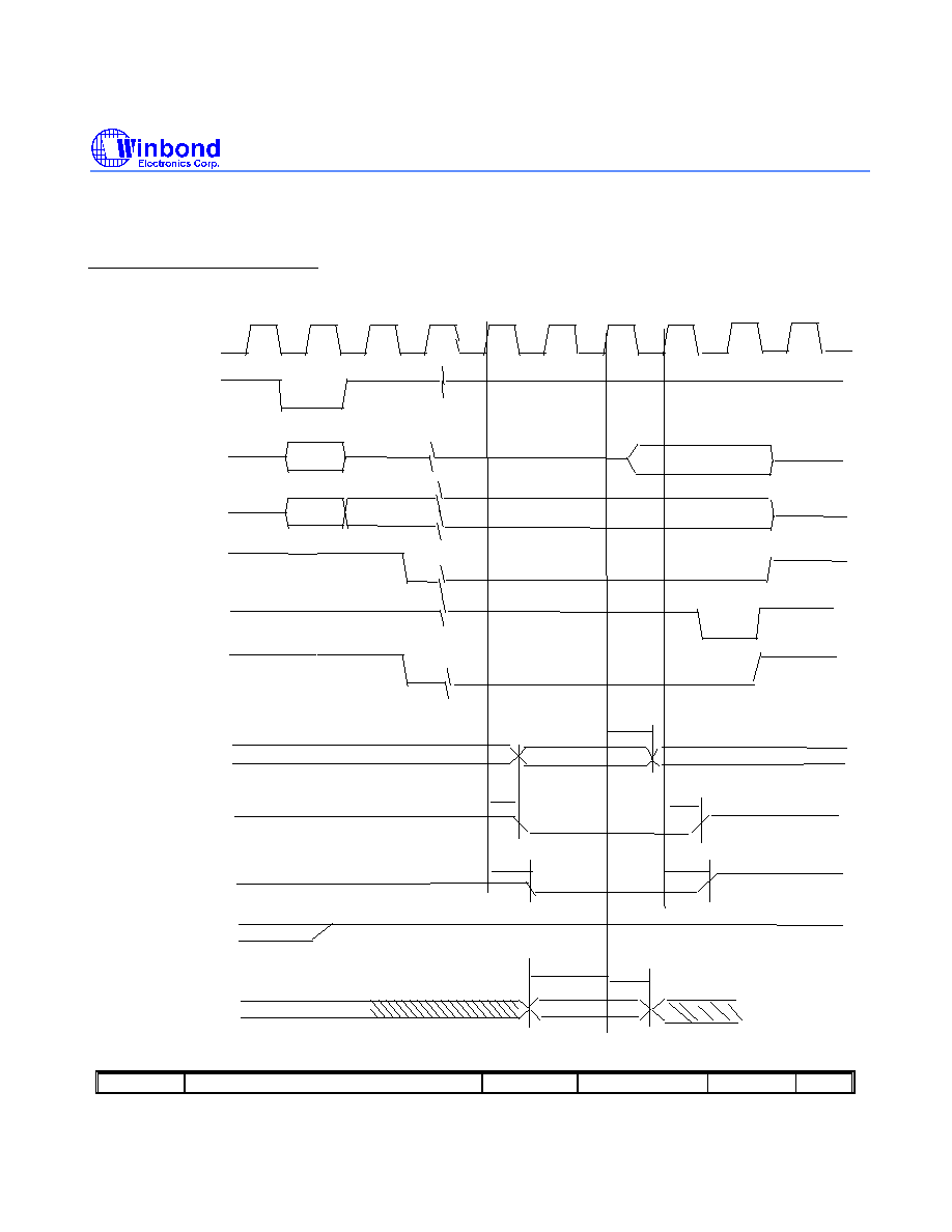
W89C940
40
MEMORY SUPPORT BUS ACCESS
32KX8-20 SRAM
Remote Read Byte Access Cycle
CLK
1
2
FRAME#
AD[31::0]
ADDRESS
BUS CMD
BE#'s
TRDY#
IRDY#
C_BE#[3:0]
DATA
DEVSEL#
MSRDB
RCSB
MSA0-13
MSWRB
(Read)
MSD0-7
0
T2
T1
T4
T3
T5
n+4
n+7
n+8
n+9
T6
T7
n+5
n+6
SYMBOL
DESCRIPTION
MIN
TYPICAL
MAX
UNIT
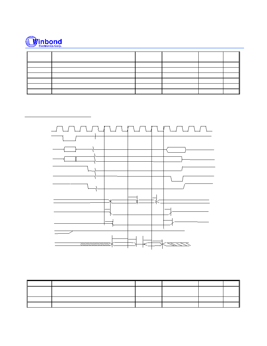
W89C940
41
T1
clock n+4 to RCSB and MSA valid (note
2)
20
25
30
nsec
T2
clock n+6 to MSA valid
25
28
30
nsec
T3
clock n+7 to RCSB deasserted time
10
15
20
nsec
T4
clock n+4 to MSRDB valid
22
27
30
nsec
T5
clock n+7 to MSRDB deasserted time
15
20
25
nsec
T6
MSD setup tim to clock n+6
7
nsec
T7
MSD hold time from clock n+6
0
nsec
Remote Read Word Access Cycle
CLK
1
2
3
FRAME#
AD[31::0]
ADDRESS
BUS CMD
BE#'s
TRDY#
IRDY#
C_BE#[3:0]
DEVSEL#
MSRDB
RCSB
MSA0-13
MSWRB
(Read)
MSD0-7
0
T2
T1
T4
n+4
n+5
n+6
DATA
T8
T3
T5
n+9
n+10
n+11
T6
T7
T7
T6
n+8
Note: 1) The other timing requirements for PCI signal are as the read transaction timing.
2) n=0,1,2,3,..... when local DMA get the control of the bus, PCI bus will insert wait state.
Wait state number is n.
SYMBOL
DESCRIPTION
MIN
TYPICAL
MAX
UNIT
T1
clock n+4 to RCSB and MSA valid (note
2)
20
25
30
nsec
T2
clock n+6 to MSA valid
25
28
30
nsec
T3
clock n+7 to RCSB deasserted time
10
15
20
nsec
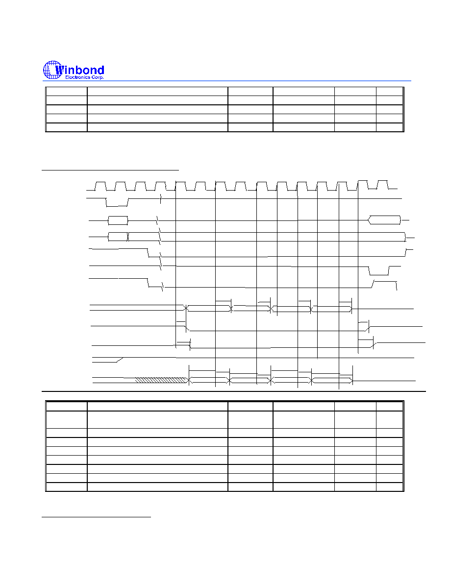
W89C940
42
T4
clock n+4 to MSRDB valid
22
27
30
nsec
T5
clock n+7 to MSRDB deasserted time
15
20
25
nsec
T6
MSD setup tim to clock n+6
7
nsec
T7
MSD hold time from clock n+6
0
nsec
T8
MSD hold time from clock n+8
nsec
Remote Read Double Word Access Cycle
CLK
1
2
3
FRAME#
AD[31::0]
ADDRESS
BUS CMD
BE#'s
TRDY#
IRDY#
C_BE#[3:0]
DATA
DEVSEL#
MSRDB
RCSB
MSA0-13
MSWRB
(Read)
MSD0-7
0
T1
T4
T3
n+4
n+5
n+6
n+7
T2
T8
n+8
n+9
T5
T6
T7
T7
T6
T6
T7
T7
T6
T2
T8
n+10 n+11 n+12 n+13 n+14
SYMBOL
DESCRIPTION
MIN
TYPICAL
MAX
UNIT
T1
clock n+4 to RCSB and MSA valid (note
2)
20
25
30
nsec
T2
clock n+6 to MSA valid
25
28
30
nsec
T3
clock n+7 to RCSB deasserted time
10
15
20
nsec
T4
clock n+4 to MSRDB valid
22
27
30
nsec
T5
clock n+7 to MSRDB deasserted time
15
20
25
nsec
T6
MSD setup tim to clock n+6
7
nsec
T7
MSD hold time from clock n+6
0
nsec
T8
MSD hold time from clock n+8
nsec
Remote Write Byte Access Cycle
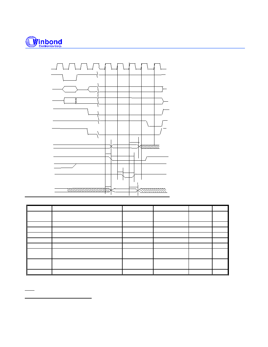
W89C940
43
CLK
1
2
3
FRAME#
AD[31::0]
ADDRESS
BUS CMD
DATA
BE#'s
TRDY#
IRDY#
C_BE[3:0]#
DATA
BE#'s
DEVSEL#
T2
MSA0-13
T1
MSRDB
RCSB
MSD0-7
MSWRB
T4
T3
T5
T6
0
n+5
n+6
n+7
n+8
n+9
T7
SYMBOL
DESCRIPTION
MIN
TYPICAL
MAX
UNIT
T1
Clock n+5 to MSA, RCSB, and
MSD valid (note 2)
17
22
27
nsec
T2
clock n+7 to MSA valid
14
19
24
nsec
T3
clock n+6 to MSWRB valid
9
14
19
nsec
T4
Write pulse width
4
9
14
nsec
T5
clock n+5 to MSD valid
7
12
17
nsec
T6
clock n+7 to MSD deasserted
14
19
24
nsec
T7
MSA change to MSWRB
deasserted time
17
22
27
nsec
T8
clock n+7/ n+9 to MSD
deasserted
16
21
26
nsec
T9
clock n+9 to MSD deasserted
8
13
18
nsec
File4
Remote Write Word Access Cycle

W89C940
44
CLK
1
2
3
FRAME#
AD[31::0]
ADDRESS
BUS CMD
DATA
BE#'s
TRDY#
IRDY#
C_BE[3:0]#
DATA
BE#'s
DEVSEL#
T2
T5
MSA0-13
T1
MSRDB
RCSB
MSD0-7
MSWRB
T4
T3
T7
T6
T8
0
n+5
n+6
n+7
n+8
n+9
n+10
n+11
T9
T4
T3
T10
T11
Note: 1) The other timing requirements for PCI signal are as the read transaction timing.
2) n=0,1,2,3,..... when local DMA get the control of the bus, PCI bus will insert wait state.
Wait state number is n.
SYMBOL
DESCRIPTION
MIN
TYPICAL
MAX
UNIT
T1
Clock n+5 to MSA, RCSB, and
MSD valid (note 2)
17
22
27
nsec
T2
clock n+7 to MSA valid
14
19
24
nsec
T3
clock n+6 to MSWRB valid
9
14
19
nsec
T4
Write pulse width
4
9
14
nsec
T5
clock n+10 to RCSB deasserted
7
12
17
nsec
T6
clock n+9 to MSA deasserted
14
19
24
nsec
T7
clock n+5 to MSD valid
17
22
27
nsec
T8
clock n+7 to MSD deasserted
16
21
26
nsec
T9
clock n+10 to MSD deasserted
8
13
18
nsec
T10
MSA change to MSWRB
deasserted time
T11
MSA change to MSWRB
deasserted time

W89C940
45
Remote Write Double Word Access Cycle
CLK
1
2
3
FRAME#
AD[31::0]
ADDRESS
BUS CMD
DATA
BE#'s
TRDY#
IRDY#
C_BE[3:0]#
DATA
BE#'s
DEVSEL#
T2
MSA0-13
T1
MSRDB
RCSB
MSD0-7
MSWRB
T7
T6
T5
0
n+5
n+6
n+7
n+8
n+9
n+10
n+11
T8
T9
T4
T3
T4
T3
T10
T11
T8
T9
T4
T3
T4
T3
n+12 n+13
n+14 n+15
SYMBOL
DESCRIPTION
MIN
TYPICAL
MAX
UNIT
T1
Clock n+5 to MSA, RCSB, and
MSD valid (note 2)
17
22
27
nsec
T2
clock n+7 to MSA valid
14
19
24
nsec
T3
clock n+6 to MSWRB valid
9
14
19
nsec
T4
Write pulse width
4
9
14
nsec
T5
clock n+11 to RCSB deasserted
7
12
17
nsec
T6
clock n+10 to MSA deasserted
14
19
24
nsec
T7
clock n+5 to MSD valid
17
22
27
nsec
T8
clock n+7 to MSD deasserted
16
21
26
nsec
T9
clock n+9 to MSD deasserted
8
13
18
nsec
T10
MSA change to MSWRB
deasserted time
T11
MSA change to MSWRB
deasserted time
32KX8-70 SRAM
Remote Read Byte Access Cycle
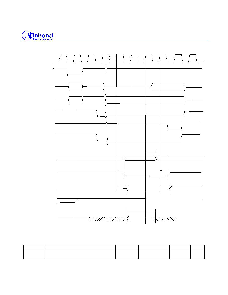
W89C940
46
CLK
1
2
FRAME#
AD[31::0]
ADDRESS
BUS CMD
BE#'s
TRDY#
IRDY#
C_BE#[3:0]
DATA
DEVSEL#
MSRDB
RCSB
MSA0-13
MSWRB
(Read)
MSD0-7
0
T2
T1
T4
T3
T5
n+4
n+7
n+8
n+9
T6
T7
n+5
n+6
SYMBOL
DESCRIPTION
MIN
TYPICAL
MAX
UNIT
T1
clock n+4 to RCSB and MSA valid (note
2)
20
25
30
nsec
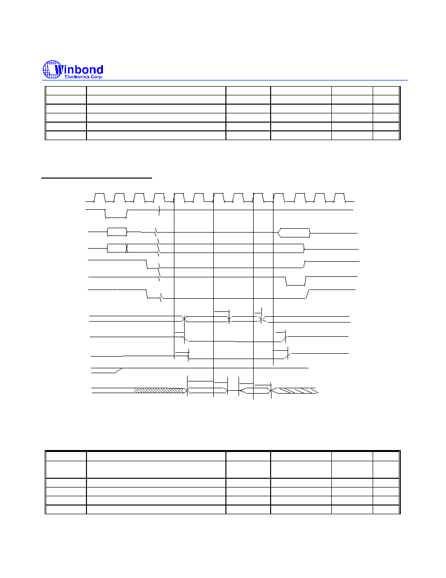
W89C940
47
T2
clock n+6 to MSA valid
25
28
30
nsec
T3
clock n+7 to RCSB deasserted time
10
15
20
nsec
T4
clock n+4 to MSRDB valid
22
27
30
nsec
T5
clock n+7 to MSRDB deasserted time
15
20
25
nsec
T6
MSD setup tim to clock n+6
7
nsec
T7
MSD hold time from clock n+6
0
nsec
Remote Read Word Access Cycle
CLK
1
2
3
FRAME#
AD[31::0]
ADDRESS
BUS CMD
BE#'s
TRDY#
IRDY#
C_BE#[3:0]
DEVSEL#
MSRDB
RCSB
MSA0-13
MSWRB
(Read)
MSD0-7
0
T2
T1
T4
n+4
n+5
n+6
DATA
T8
T3
T5
n+9
n+10
n+11
T6
T7
T7
T6
n+8
Note: 1) The other timing requirements for PCI signal are as the read transaction timing.
2) n=0,1,2,3,..... when local DMA get the control of the bus, PCI bus will insert wait state.
Wait state number is n.
SYMBOL
DESCRIPTION
MIN
TYPICAL
MAX
UNIT
T1
clock n+4 to RCSB and MSA valid (note
2)
20
25
30
nsec
T2
clock n+6 to MSA valid
25
28
30
nsec
T3
clock n+7 to RCSB deasserted time
10
15
20
nsec
T4
clock n+4 to MSRDB valid
22
27
30
nsec
T5
clock n+7 to MSRDB deasserted time
15
20
25
nsec
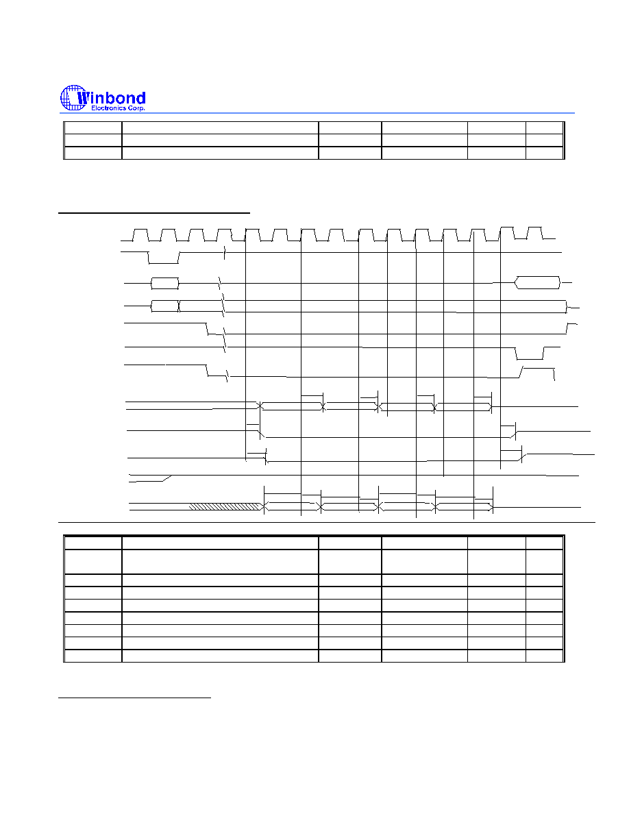
W89C940
48
T6
MSD setup tim to clock n+6
7
nsec
T7
MSD hold time from clock n+6
0
nsec
T8
MSD hold time from clock n+8
nsec
Remote Read Double Word Access Cycle
CLK
1
2
3
FRAME#
AD[31::0]
ADDRESS
BUS CMD
BE#'s
TRDY#
IRDY#
C_BE#[3:0]
DATA
DEVSEL#
MSRDB
RCSB
MSA0-13
MSWRB
(Read)
MSD0-7
0
T1
T4
T3
n+4
n+5
n+6
n+7
T2
T8
n+8
n+9
T5
T6
T7
T7
T6
T6
T7
T7
T6
T2
T8
n+10 n+11 n+12 n+13 n+14
SYMBOL
DESCRIPTION
MIN
TYPICAL
MAX
UNIT
T1
clock n+4 to RCSB and MSA valid (note
2)
20
25
30
nsec
T2
clock n+6 to MSA valid
25
28
30
nsec
T3
clock n+7 to RCSB deasserted time
10
15
20
nsec
T4
clock n+4 to MSRDB valid
22
27
30
nsec
T5
clock n+7 to MSRDB deasserted time
15
20
25
nsec
T6
MSD setup tim to clock n+6
7
nsec
T7
MSD hold time from clock n+6
0
nsec
T8
MSD hold time from clock n+8
nsec
Remote Write Byte Access Cycle
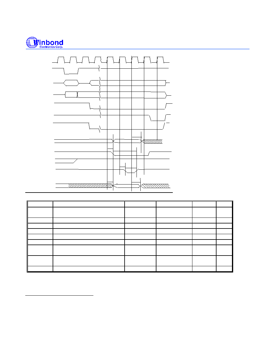
W89C940
49
CLK
1
2
3
FRAME#
AD[31::0]
ADDRESS
BUS CMD
DATA
BE#'s
TRDY#
IRDY#
C_BE[3:0]#
DATA
BE#'s
DEVSEL#
T2
MSA0-13
T1
MSRDB
RCSB
MSD0-7
MSWRB
T4
T3
T5
T6
0
n+5
n+6
n+7
n+8
n+9
T7
SYMBOL
DESCRIPTION
MIN
TYPICAL
MAX
UNIT
T1
Clock n+5 to MSA, RCSB, and
MSD valid (note 2)
17
22
27
nsec
T2
clock n+7 to MSA valid
14
19
24
nsec
T3
clock n+6 to MSWRB valid
9
14
19
nsec
T4
Write pulse width
4
9
14
nsec
T5
clock n+5 to MSD valid
7
12
17
nsec
T6
clock n+7 to MSD deasserted
14
19
24
nsec
T7
MSA change to MSWRB
deasserted time
17
22
27
nsec
T8
clock n+7/ n+9 to MSD
deasserted
16
21
26
nsec
T9
clock n+9 to MSD deasserted
8
13
18
nsec
Remote Write Word Access Cycle
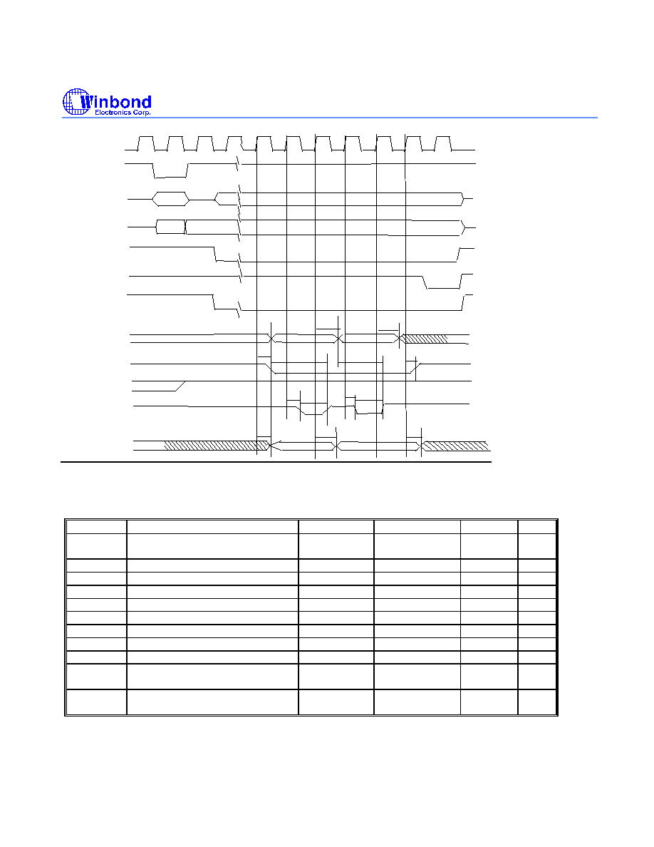
W89C940
50
CLK
1
2
3
FRAME#
AD[31::0]
ADDRESS
BUS CMD
DATA
BE#'s
TRDY#
IRDY#
C_BE[3:0]#
DATA
BE#'s
DEVSEL#
T2
T5
MSA0-13
T1
MSRDB
RCSB
MSD0-7
MSWRB
T4
T3
T7
T6
T8
0
n+5
n+6
n+7
n+8
n+9
n+10
n+11
T9
T4
T3
T10
T11
Note: 1) The other timing requirements for PCI signal are as the read transaction timing.
2) n=0,1,2,3,..... when local DMA get the control of the bus, PCI bus will insert wait state.
Wait state number is n.
SYMBOL
DESCRIPTION
MIN
TYPICAL
MAX
UNIT
T1
Clock n+5 to MSA, RCSB, and
MSD valid (note 2)
17
22
27
nsec
T2
clock n+7 to MSA valid
14
19
24
nsec
T3
clock n+6 to MSWRB valid
9
14
19
nsec
T4
Write pulse width
4
9
14
nsec
T5
clock n+10 to RCSB deasserted
7
12
17
nsec
T6
clock n+9 to MSA deasserted
14
19
24
nsec
T7
clock n+5 to MSD valid
17
22
27
nsec
T8
clock n+7 to MSD deasserted
16
21
26
nsec
T9
clock n+10 to MSD deasserted
8
13
18
nsec
T10
MSA change to MSWRB
deasserted time
T11
MSA change to MSWRB
deasserted time
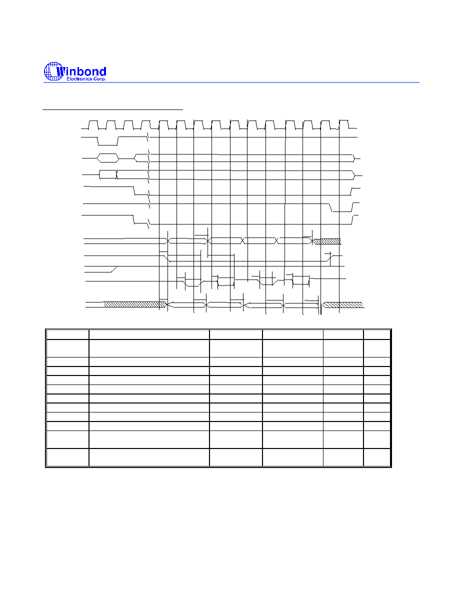
W89C940
51
Remote Write Double Word Access Cycle
CLK
1
2
3
FRAME#
AD[31::0]
ADDRESS
BUS CMD
DATA
BE#'s
TRDY#
IRDY#
C_BE[3:0]#
DATA
BE#'s
DEVSEL#
T2
MSA0-13
T1
MSRDB
RCSB
MSD0-7
MSWRB
T7
T6
T5
0
n+5
n+6
n+7
n+8
n+9
n+10
n+11
T8
T9
T4
T3
T4
T3
T10
T11
T8
T9
T4
T3
T4
T3
n+12 n+13
n+14 n+15
SYMBOL
DESCRIPTION
MIN
TYPICAL
MAX
UNIT
T1
Clock n+5 to MSA, RCSB, and
MSD valid (note 2)
17
22
27
nsec
T2
clock n+7 to MSA valid
14
19
24
nsec
T3
clock n+6 to MSWRB valid
9
14
19
nsec
T4
Write pulse width
4
9
14
nsec
T5
clock n+11 to RCSB deasserted
7
12
17
nsec
T6
clock n+10 to MSA deasserted
14
19
24
nsec
T7
clock n+5 to MSD valid
17
22
27
nsec
T8
clock n+7 to MSD deasserted
16
21
26
nsec
T9
clock n+9 to MSD deasserted
8
13
18
nsec
T10
MSA change to MSWRB
deasserted time
T11
MSA change to MSWRB
deasserted time
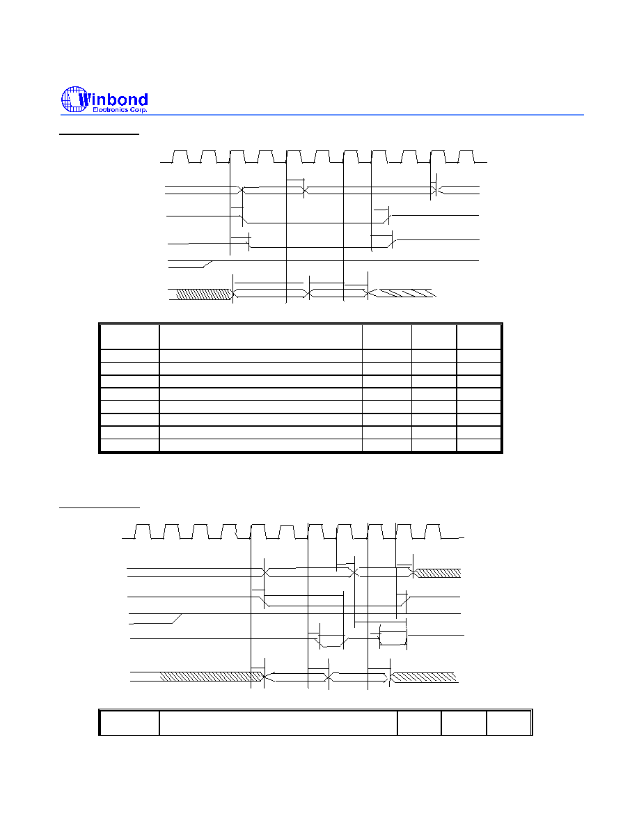
W89C940
52
Local Read cycle
CLK
1
2
3
4
5
6
7
8
MSRDB
RCSB
MSA0-13
MSWRB
(Read)
MSD0-7
T2
T1
T4
T8
T3
T5
T6
T7
T7
T6
SYMBOL
DESCRIPTION
MIN
TYPIC
AL
MAX
T1
clock 1 to RCSB and MSA valid (note 2)
4
8
12
T2
clock 3 to MSA valid
20
24
28
T3
clock 6 to RCSB deasserted time
4
8
12
T4
clock 1 to MSRDB valid
8
12
16
T5
clock 6 to MSRDB deasserted time
8
12
16
T6
MSD setup tim to clock 3
24
28
32
T7
MSD hold time from clock 3
24
28
32
T8
MSD hold time from clock 8
Local Write cycle
CLK
1
2
3
0
1
2
3
4
5
6
7
T2
T5
MSA0-13
T1
MSRDB
RCSB
MSD0-7
MSWRB
T7
T6
T8
T9
T3
T4
T3
T4
T10
T11
SYMBOL
DESCRIPTION
MIN
TYPIC
AL
MAX
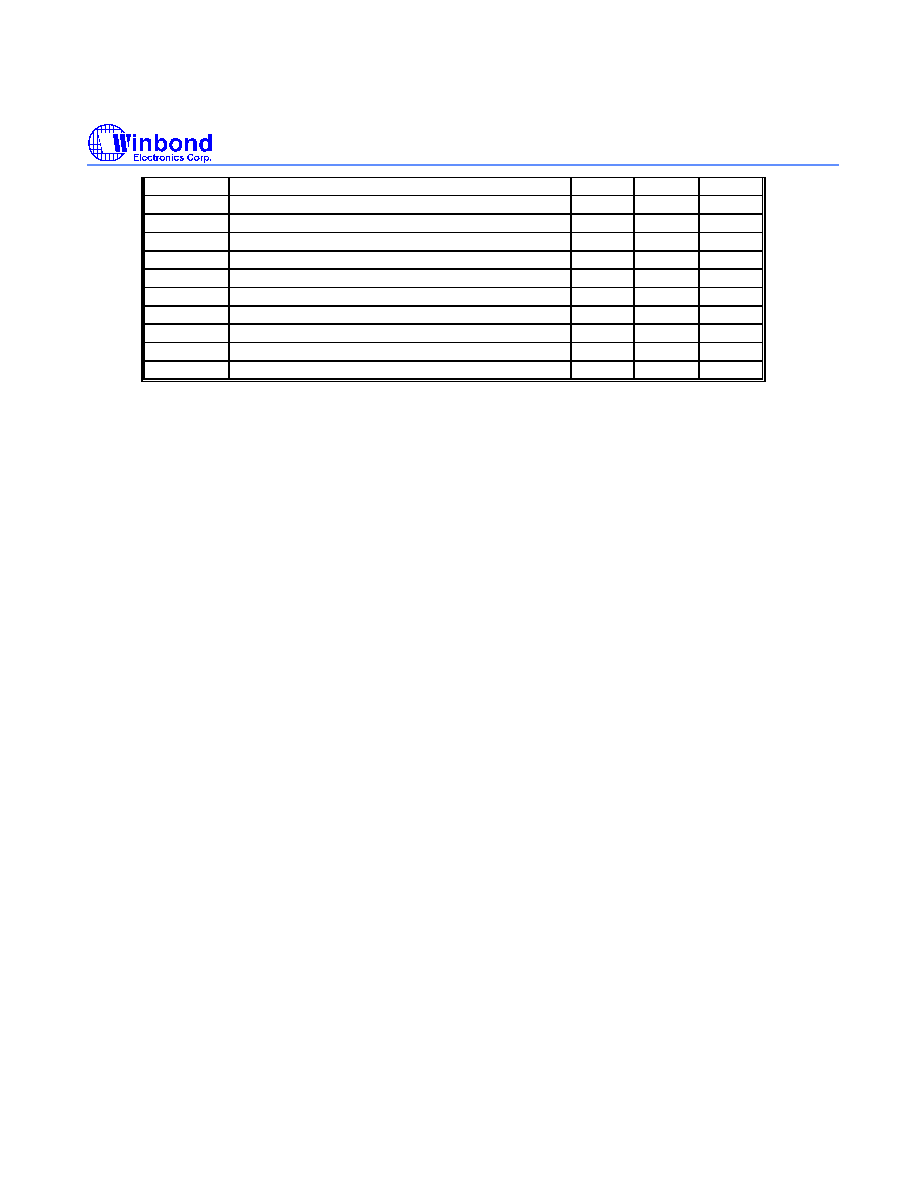
W89C940
53
T1
Clock 1 to MSA and RCSB valid
16
20
24
T2
clock 4 to MSA valid
4
8
12
T3
clock 3 to MSWRB valid
4
8
12
T4
Write pulse width
20
24
28
T5
clock 6 to RCSB deasserted
20
24
28
T6
clock 6 to MSA deasserted
T7
clock 1 to MSD valid
T8
clock 3 to MSD deasserted
8
12
16
T9
clock 5 to MSD deasserted
8
12
16
T10
MSA valid to MSWRB deasserted
64
68
72
T11
MSA valid to MSWRB deasserted
40
44
48
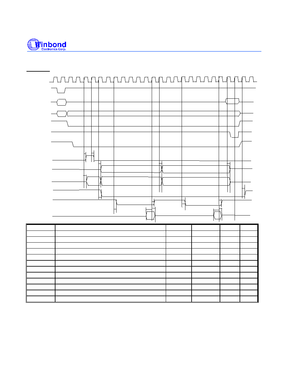
W89C940
54
32KX8-220 BPROM/ FLASH MEMORY
Read cycle
CLK
FRAME#
AD[31::0]
TRDY#
IRDY#
C_BEB[3:0]#
DEVSEL#
MSA14/L
MSA[9:0]
MSA[13:10]
BPCSB
MSRDB
MSD[7:0]
0
1
2
3
4
5
6
7
8
9 10 11 12 13 14 15 16 17 18 19 20 21 22 23 24 25 26
T1
T2
T3
T4
T5
T6
T7
T8
T9
T10
T11
T12
T9
T10
T11
T12
SYMBOL
DESCRIPTION
MIN
TYPICAL
MAX
UNIT
T1
clock 4 to MSA14/L valid
8
13
18
nsec
T2
clock 5 to MSA14/L deasserted time
8
13
18
nsec
T3
clock 6 to MSA bus valid
8
13
18
nsec
T4
clock 14 to MSA bus valid
8
13
18
nsec
T5
clock 23 to MSA deasserted
8
13
18
nsec
T6
clock 4 to MSA high nibble valid
8
13
18
nsec
T7
clock 6 to BPCSB valid
15
20
25
nsec
T8
clock 25 to BPCSB deasserted
7
12
17
nsec
T9
clock 8/ clock 17 to MSRDB asserted time
15
20
25
nsec
T10
clock 13/ clock 22 to MSRDB deasserted time
8
13
18
nsec
T11
MSD setup time from clock 13
7
nsec
T12
MSD hold time from clock 15
0
nsec
Note: 1) The other timing requirements for PCI signal are as the read transaction timing.
2) BPROM/FLASH memory access could be byte, word or double word access.
The timing is the same.

W89C940
55
FILE5
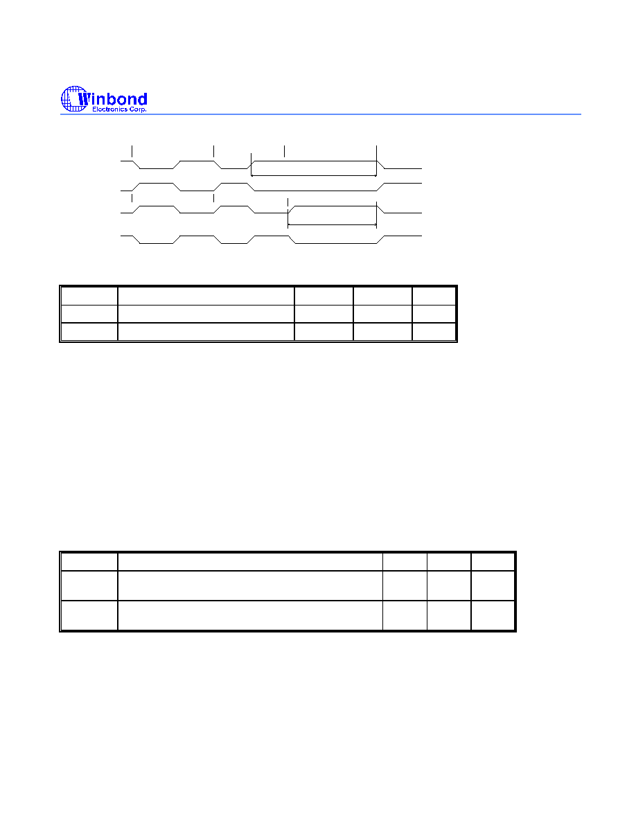
W89C940
56
AUI/UTP TIMING
AUI Transmit Timing (End of
Transmit)
SYMBOL
DESCRIPTION
MIN.
MAX.
UNIT
Ttoh
Transmit Output High Before Idle
200
nS
Ttoi
Transmit Output Idle Time
8000
nS
AUI/UTP RECEIVE TIMING (END OF RECEIVE)
SYMBOL
DESCRIPTION
MIN.
MAX.
UNIT
T
eop1
End of Packet Received Hold Time after Logic "1"
(Note 1)
200
nS
T
eop0
End of Packet Received Hold Time after Logic "0"
(Note 1)
200
nS
Note 1: This parameter is specified by design and is not tested.
Ttoi
0
Ttoh
1
0
TXP/N
TXP/N
1
0
1
1
1
RXP/XRDP
RXN/XRDM
RXP/XRDP
0
0
Teop1
Teop0
RXN/XRDM
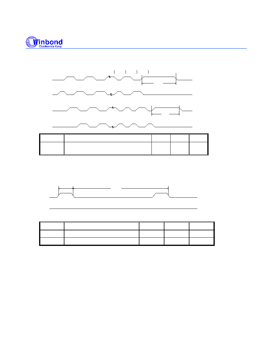
W89C940
57
TPI TRANSMIT TIMING (END OF TRANSMIT)
0
1
Teth1
1
Teth1
TPDP
TPDM
TPDP
TPDM
SYMBOL
DESCRIPTION
MIN.
MAX.
UNIT
T
eth1
End of Packet Transmitted Hold Time 1
(TPDP/M) (Note 1)
250
nS
Link Pulse Timing
Tlpi
Tlpw
TPDP
TPDM
SYMBOL
DESCRIPTION
MIN.
MAX.
UNIT
T
lpi
Link Output Pulse Interval
8
24
mS
T
lpw
Link Output Pulse Width
80
120
nS
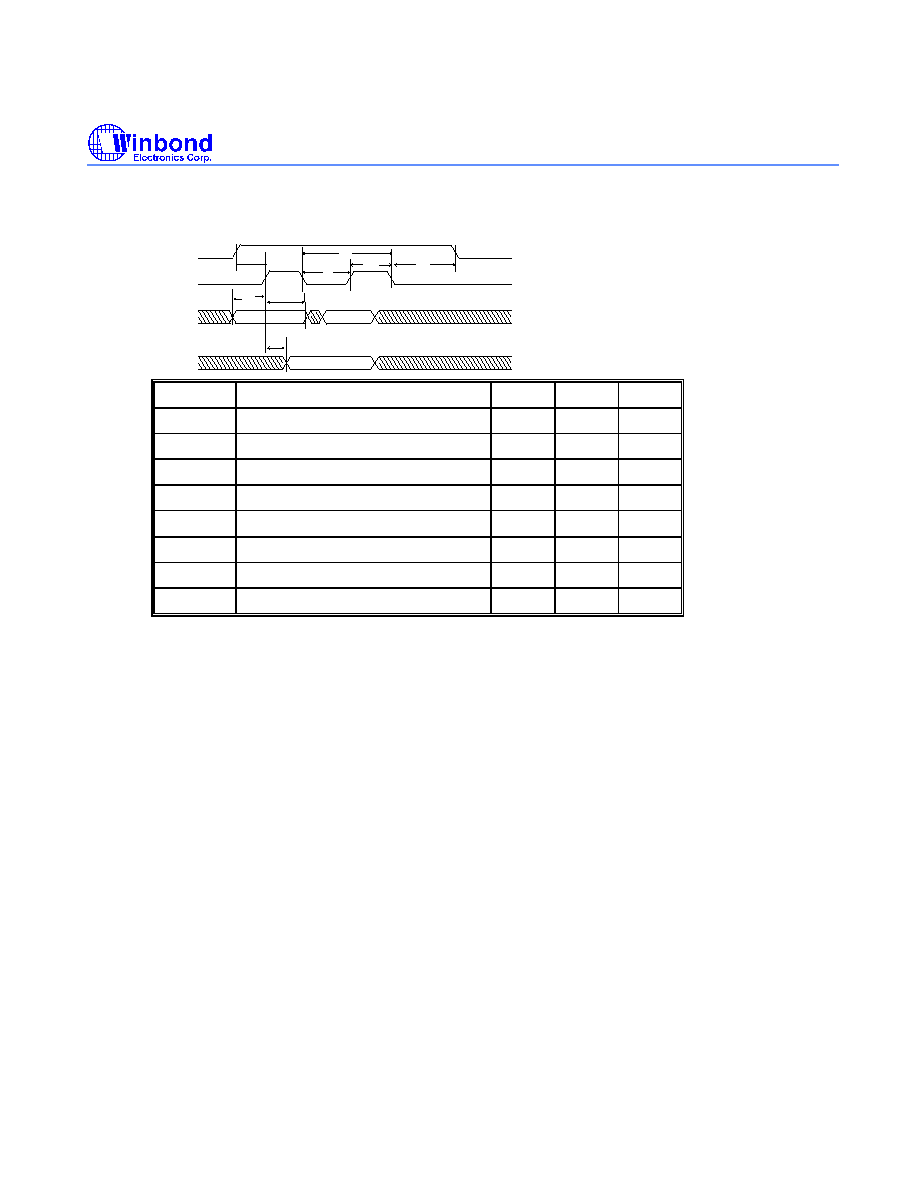
W89C940
58
Serial EEPROM Timing
SYMBOL
DESCRIPTION
MIN.
MAX.
UNIT
T1
EECS asserted to SK
500
nS
T2
EECS hold from SK
0
500
nS
T3
MSD2 OFF time
500
600
nS
T4
MSD2 ON time
500
600
nS
T5
MSD2 clock period
1
1.2
µ
S
T6
MSD1 set up time to MSD2 high
500
600
nS
T7
MSD1 hold time from MSD2 high
500
600
nS
T8
MSD0 valid from MSD2 high
300
nS
T2
T1
T5
EECS
T6
MSD2
MSD1
MSD0
T8
T3
T7
T4
(SCK)
(DO)
(DI)
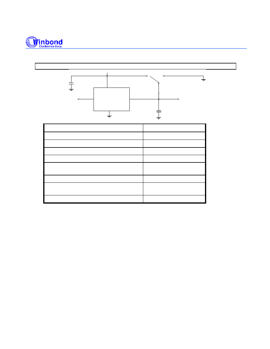
W89C940
59
AC TIMING
TEST
CONDITIONS
PARAMETER
TEST CONDITION
Supply voltage (V
DD
/V
SS
)
5V
±
5%
Temperature
25
∞
C/70
∞
C
Input Test Pattern Levels (TTL/CMOS)
GND to 4.0V
Input Rise and Fall Times (TTL/CMOS)
5nS
Input and Output Pattern Reference Level
(TTL/CMOS)
1.5V
Input Waveform Level (Diff)
-350 to -1315 mV
Input and Output Waveform
Reference Levels
50% Point of the Differential
Tristate Reference Levels
Float (V) + 0.5V
Note 1: These parameters are specified by design and are not tested.
OUTPUT LOAD
The above specifications are valid only if the mandatory isolations are correctly employed and all differential
signals are taken to the AUI of the pulse transformer.
Note 1: Load capacitance employed depends on output type.
For 3SL, MOS, TPI, AUI: CL=50 pF.
For 3SH, OCH: CL=240 pF.
Note 2: Specifications which measure delays from an active state to a High-Z state are not guaranteed by production test, but are characterized
using 240 pF and are correlated to determine true driver turn-off time by eliminating inherent R-C delay
times in measurements.
Note 3: SW1=Open for push pull outputs during timing test.
SW1=VCC for VOL test.
SW1=GND for VOH test.
SW1=VCC for High-Z to active low and active low to High-Z measurements.
SW1=GND for High-Z to active high and active high to High-Z measurements.
SW1 (Note 3)
Vcc
0.1uF
Input
DEVICE
UNDER
TEST
RL = 2.2K
Output
CL (Note 1,2)
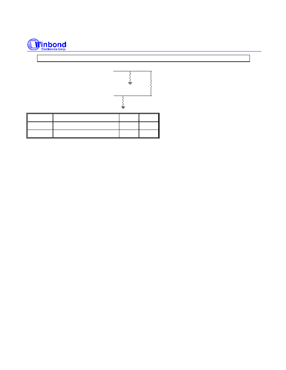
W89C940
60
Pin Capacitance
TA = 25
∞
C f = 1 MHz
SYMBOL
PARAMETER
TYP
UNIT
C
IN
Input Capacitance
7
pF
C
OUT
Output Capacitance
10
p
DERATING FACTOR
Output timing is measured with a purely capacitive load of 50pF or 240pF.
The following correction factor can be used for other loads (this factor is preliminary only):
Derating for 3SL, MOS = -0.05 nS/pF.
Derating for 3SH, OCL, TPI = -0.03 nS/pF.
AUI TRANSMIT TEST LOAD
Note: In the above diagram, the TX+ and TX- signals are taken from the AUI side of the pulse transformer.
The pulse transformer used for all testing is a 100
µ
H +/-0.1% Pulse Engineering PE64103.
PACKAGE DIMENSIONS
DOP
DON
R=270
R=270
R=78
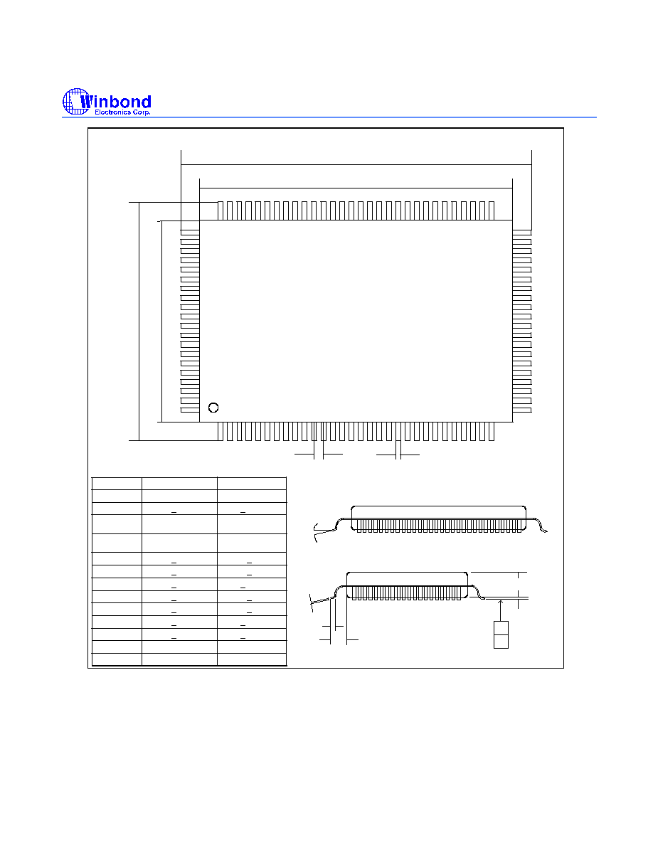
W89C940
61
100 PINS PQFP
He
E
Hd
D
e
b
Symbol
A1
A2
b
C
D
E
e
Hd
He
L
L1
Y
@
Dimension in inch
Dimension in mm
0.004 min
0.112 + 0.005
+
+
+
0.012+ 0.004
- 0.002
0.006+ 0.004
0.551
0.787
0.026
+
+
+
+
0.740
0.976
0.047
0.095
0.004 MAX
0.008
0.008
0.012
0.012
0.006
0.005
0.005
- 0.002
0 -------- 12
0.102 min
2.845 + 0.127
+
+
+
0.350+ 0.102
- 0.051
0.152+ 0.102
14.000
20.000
0.650
+
+
+
+
18.796
24.790
1.194
2.413
0.102 MAX
0.203
0.203
0.305
0.305
0.152
0.127
0.127
- 0.051
0 -------- 12
@
C
L1
L
A2
A1
D
Y