Document Outline
- GENERAL DESCRIPTION
- FEATURES
- KEY PARAMETERS
- PIN CONFIGURATION
- PIN DESCRIPTION
- BLOCK DIAGRAM
- ELECRICAL CHARACTERISTICS
- OPERATION MODE
- FUNCTIONAL DESCRIPTION
- TIMING WAVEFORMS
- Command Input Timing
- Timing of the CLK Signals
- Read Timing (Burst Length = 4)
- Write Timing (Burst Length = 4)
- DM, Data Mask (W942508CH /W942504CH)
- DM, Data Mask (W942516CH)
- Mode Register Set (MRS) Timing
- Extend Mode Register Set (EMRS) Timing
- Auto Precharge Timing (Read Cycle, CL = 2)
- Auto Precharge Timing (Write Cycle)
- Read Interrupted by Read (CL = 2, BL = 2, 4, 8)
- Burst Read Stop (BL = 8)
- Read Interrupted by Write & BST (BL = 8)
- Read Interrupted by Precharge (BL = 8)
- Write Interrupted by Write (BL = 2, 4, 8)
- Write Interrupted by Read (CL = 2, BL = 8)
- Write Interrupted by Read (CL = 2.5, BL = 4)
- Write Interrupted by Precharge (BL = 8)
- 2 Bank Interleave Read Operation (CL = 2, BL = 2)
- 2 Bank Interleave Read Operation (CL = 2, BL = 4)
- 4 Bank Interleave Read Operation (CL = 2, BL = 2)
- 4 Bank Interleave Read Operation (CL = 2, BL = 4)
- Auto Refresh Cycle
- Active Power Down Mode Entry and Exit Timing
- Precharged Power Down Mode Entry and Exit Timing
- Self Refresh Entry and Exit Timing
- PACKAGE DIMENSION
- REVISION HISTORY

W942516CH
4M
� 4 BANKS � 16 BIT DDR SDRAM
Publication Release Date: May 20, 2003
- 1 -
Revision A2
Table of Contents-
1.
GENERAL DESCRIPTION ......................................................................................................... 3
2.
FEATURES ................................................................................................................................. 3
3.
KEY PARAMETERS ................................................................................................................... 4
4.
PIN CONFIGURATION ............................................................................................................... 5
5.
PIN DESCRIPTION..................................................................................................................... 6
6.
BLOCK DIAGRAM ...................................................................................................................... 7
7.
ELECRICAL CHARACTERISTICS ............................................................................................. 8
7.1
Absolute Maximum Ratings ................................................................................................. 8
7.2
Recommended DC Operating Conditions............................................................................ 8
7.3
Capacitance ......................................................................................................................... 9
7.4
Leakage and Output Buffer Characteristics ......................................................................... 9
7.5
DC Characteristics ............................................................................................................. 10
7.6
AC Characteristics and Operating Condition ..................................................................... 11
7.7
AC Test Conditions ............................................................................................................ 13
8.
OPERATION MODE ................................................................................................................. 15
8.1
Simplified Truth Table ........................................................................................................ 15
8.2
Function Truth Table .......................................................................................................... 16
8.3
Function Truth Table for CKE ............................................................................................ 19
8.4
Simplified Stated Diagram.................................................................................................. 20
9.
FUNCTIONAL DESCRIPTION.................................................................................................. 21
9.1
Power Up Sequence .......................................................................................................... 21
9.2
Command Function............................................................................................................ 21
9.3
Read Operation.................................................................................................................. 24
9.4
Write Operation .................................................................................................................. 24
9.5
Precharge........................................................................................................................... 24
9.6
Burst Termination............................................................................................................... 25
9.7
Refresh Operation.............................................................................................................. 25
9.8
Power Down Mode............................................................................................................. 25
9.9
Mode Register Operation ................................................................................................... 25
10.
TIMING WAVEFORMS ............................................................................................................. 29
10.1
Command Input Timing...................................................................................................... 29
10.2
Timing of the CLK Signals.................................................................................................. 29

W942516CH
- 2 -
10.3
Read Timing (Burst Length = 4)......................................................................................... 30
10.4
Write Timing (Burst Length = 4) ......................................................................................... 31
10.5
DM, Data Mask (W942508CH /W942504CH).................................................................... 32
10.6
DM, Data Mask (W942516CH) .......................................................................................... 32
10.7
Mode Register Set (MRS) Timing ...................................................................................... 33
10.8
Extend Mode Register Set (EMRS) Timing........................................................................ 34
10.9
Auto Precharge Timing (Read Cycle, CL = 2).................................................................... 35
10.10
Auto Precharge Timing (Write Cycle)................................................................................. 37
10.11
Read Interrupted by Read (CL = 2, BL = 2, 4, 8) ............................................................... 38
10.12
Burst Read Stop (BL = 8)................................................................................................... 38
10.13
Read Interrupted by Write & BST (BL = 8)......................................................................... 39
10.14
Read Interrupted by Precharge (BL = 8)............................................................................ 39
10.15
Write Interrupted by Write (BL = 2, 4, 8) ............................................................................ 40
10.16
Write Interrupted by Read (CL = 2, BL = 8) ....................................................................... 40
10.17
Write Interrupted by Read (CL = 2.5, BL = 4) .................................................................... 41
10.18
Write Interrupted by Precharge (BL = 8) ............................................................................ 41
10.19
2 Bank Interleave Read Operation (CL = 2, BL = 2) .......................................................... 42
10.20
2 Bank Interleave Read Operation (CL = 2, BL = 4) .......................................................... 42
10.21
4 Bank Interleave Read Operation (CL = 2, BL = 2) .......................................................... 43
10.22
4 Bank Interleave Read Operation (CL = 2, BL = 4) .......................................................... 43
10.23
Auto Refresh Cycle ............................................................................................................ 44
10.24
Active Power Down Mode Entry and Exit Timing............................................................... 44
10.25
Precharged Power Down Mode Entry and Exit Timing ...................................................... 44
10.26
Self Refresh Entry and Exit Timing .................................................................................... 45
11.
PACKAGE DIMENSION ........................................................................................................... 46
12.
REVISION HISTORY ................................................................................................................ 47

W942516CH
Publication Release Date: May 20, 2003
- 3 -
Revision A2
1. GENERAL DESCRIPTION
W942516CH is a CMOS Double Data Rate synchronous dynamic random access memory (DDR
SDRAM), organized as 4,194,304 words
� 4 banks � 16 bits. Using pipelined architecture and 0.13 �m
process technology, W942516CH delivers a data bandwidth of up to 400M words per second (-5). To
fully comply with the personal computer industrial standard, W942516CH is sorted into four speed
grades: -5, -6, -7, -75 The -5 is compliant to the 200 MHz/CL2.5 & CL3 specification, The -6 is
compliant to the 166 MHz/CL2.5 specification, the -7 is compliant to the 143 MHz/CL2.5 or
DDR266/CL2 specification, the -75 is compliant to the DDR266/CL2.5 specification.
All Inputs reference to the positive edge of CLK (except for DQ, DM, and CKE). The timing reference
point for the differential clock is when the CLK and
CLK
signals cross during a transition. And Write
and Read data are synschronized with the both edges of DQS (Data Strobe).
By having a programmable Mode Register, the system can change burst length, latency cycle,
interleave or sequential burst to maximize its performance. W942516CH is ideal for main memory in
high performance applications.
2. FEATURES
� 2.5V �0.2V Power Supply for DDR266
� 2.5V �0.2V Power Supply for DDR333
� 2.6V �0.1V Power Supply for DDR400
� Up to 200 MHz Clock Frequency
� Double Data Rate architecture; two data transfers per clock cycle
� Differential clock inputs (CLK and
CLK
)
� DQS is edge-aligned with data for Read; center-aligned with data for Write
� CAS Latency: 2, 2.5 and 3
� Burst Length: 2, 4 and 8
� Auto Refresh and Self Refresh
� Precharged Power Down and Active Power Down
� Write Data Mask
� Write Latency = 1
� 8K Refresh Cycles / 64 mS
� Interface: SSTL-2
� Packaged in TSOP II 66-pin, 400 x 875 mil, 0.65 mm pin pitch
W942516CH
- 4 -
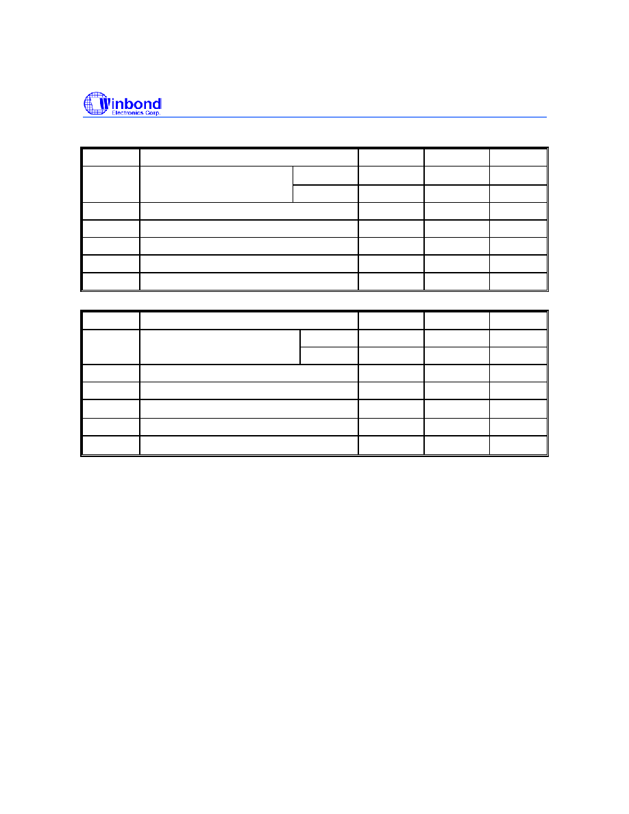
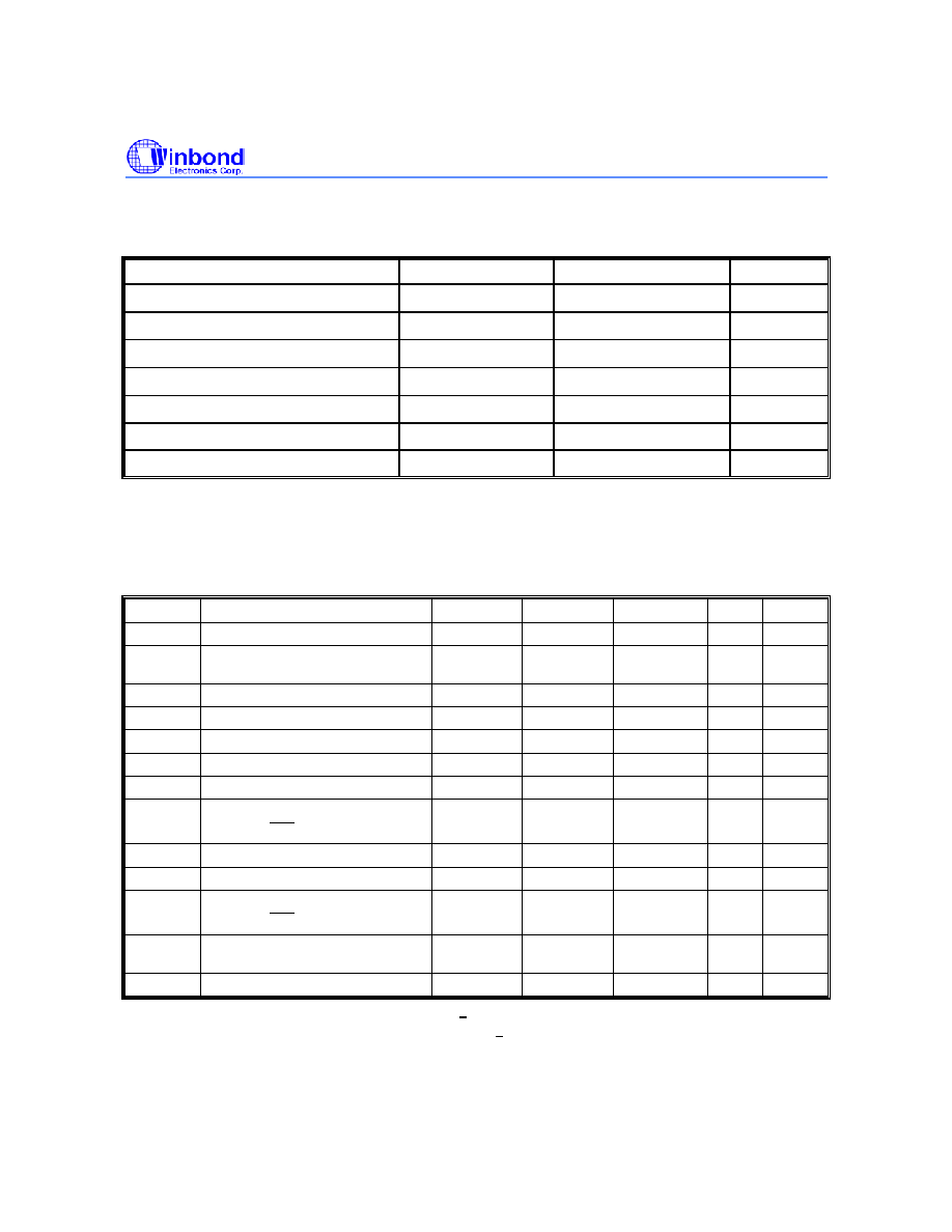
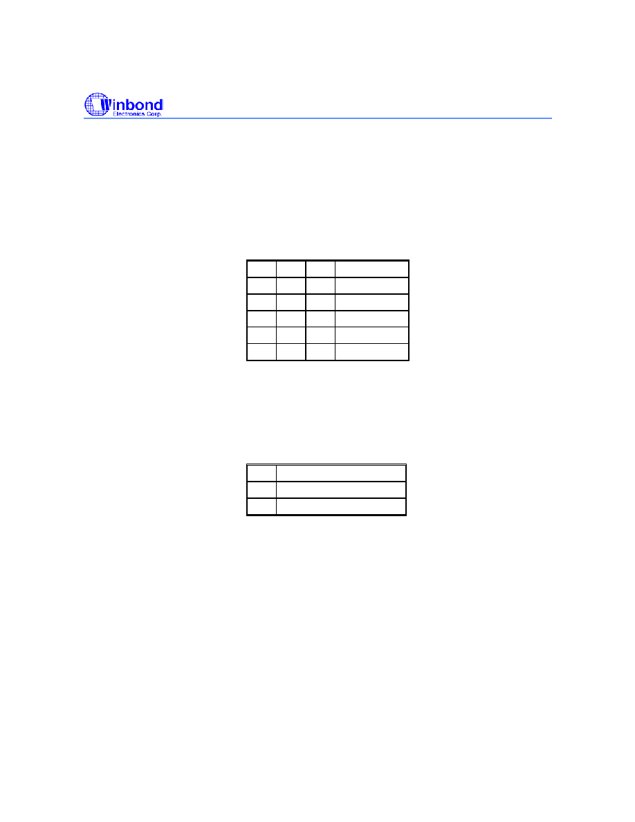
3. KEY PARAMETERS
SYMBOL
DESCRIPTION
MIN./MAX.
-7
-75
t
CK
Clock Cycle Time
CL = 2
Min.
7.5 nS
8 nS
CL = 2.5
Min.
7 nS
7.5 nS
t
RAS
Active to Precharge Command Period
Min.
45 nS
45 nS
t
RC
Active to Ref/Active Command Period
Min.
65 nS
65 nS
I
DD1
Operation Current (Single bank)
Max.
120 mA
120 mA
I
DD4
Burst Operation Current
Max.
165 mA
155 mA
I
DD6
Self-Refresh Current
Max.
3 mA
3 mA
SYMBOL
DESCRIPTION
MIN./MAX.
-5
-6
CL = 2.5
Min.
5 nS
6 nS
t
CK
Clock Cycle Time
CL = 3
Min.
5 nS
6 nS
t
RAS
Active to Precharge Command Period
Min.
40 nS
42 nS
t
RC
Active to Ref/Active Command Period
Min.
55 nS
60 nS
I
DD1
Operation Current (Single bank)
Max.
120 mA
120 mA
I
DD4
Burst Operation Current
Max.
165 mA
165 mA
I
DD6
Self-Refresh Current
Max.
3 mA
3 mA
W942516CH
Publication Release Date: May 20, 2003
- 5 -
Revision A2
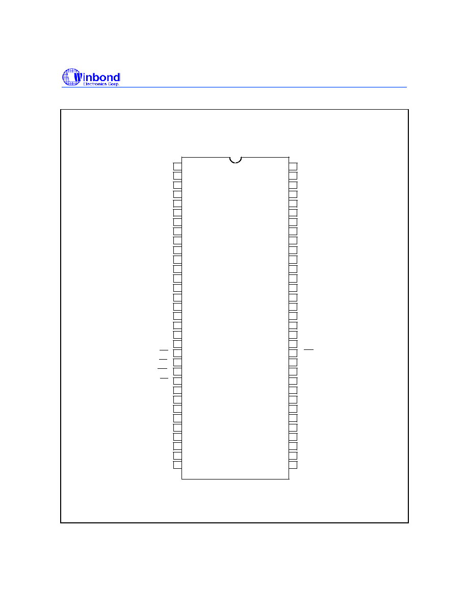
4. PIN CONFIGURATION
V
SS
DQ15
V
SS
Q
DQ14
DQ13
V
DD
Q
DQ12
DQ11
V
SS
Q
DQ10
DQ9
V
DD
Q
DQ8
V
SS
NC1
UDQS
CLK
CKE
A11
A9
A8
A7
A6
A5
A4
V
SS
66
65
64
63
62
61
60
59
58
57
56
55
54
53
52
51
50
49
48
47
46
45
44
43
42
41
40
1
2
3
4
5
6
7
8
9
10
11
12
13
14
15
16
17
18
19
20
21
22
23
24
25
26
27
V
DD
DQ0
V
DD
Q
DQ1
DQ2
V
SS
Q
DQ3
DQ4
V
DD
Q
DQ5
DQ6
V
SS
Q
DQ7
NC1
V
DD
Q
BS0
BS1
A10/AP
A0
A1
A2
A3
CS
RAS
CAS
WE
28
29
30
31
32
33
39
38
37
36
35
34
V
DD
LDM
NC1
LDQS
NC1
V
DD
NC1
V
SS
Q
NC1
A12
NC1
CLK
UDM
V
REF
W942516CH
- 6 -
5. PIN DESCRIPTION
PIN NUMBER
PIN NAME
FUNCTION
DESCRIPTION
28
- 32,
35
- 42
A0
- A12
Address
Multiplexed pins for row and column address.
Row address: A0
- A12.
Column address: A0
- A8. (A10 is used for Auto Precharge)
26, 27
BS0, BS1
Bank Select
Select bank to activate during row address latch time, or
bank to read/write during column address latch time.
2, 4, 5, 7, 8, 10,
11, 13, 54, 56, 57,
59, 60, 62, 63, 65
DQ0
-
DQ15
Data Input/ Output
The DQ0 � DQ7 input and output data are synchronized with
both edges of DQS.
16,51
LDQS,
UDQS
Data Strobe
DQS is Bi-directional signal. DQS is input signal during write
operation and output signal during read operation. It is Edge-
aligned with read data, Center-aligned with write data.
24
CS
Chip Select
Disable or enable the command decoder. When command
decoder is disabled, new command is ignored and previous
operation continues.
23, 22, 21
RAS ,
CAS ,
WE
Command Inputs Command inputs (along with
CS
) define the command
being entered.
20, 47
LDM, UDM
Write Mask
When DM is asserted "high" in burst write, the input data is
masked. DM is synchronized with both edges of DQS.
45, 46
CLK,
CLK
Differential Clock
Inputs
All address and control input signals are sampled on the
crossing of the positive edge of CLK and negative edge of
CLK
.
44 CKE
Clock
Enable
CKE controls the clock activation and deactivation. When
CKE is low, Power Down mode, Suspend mode, or Self
Refresh mode is entered.
49 V
REF
Reference
Voltage V
REF
is reference voltage for inputs.
1, 18, 33
V
DD
Power (+2.5V)
Power for logic circuit inside DDR SDRAM.
34, 48, 66
V
SS
Ground
Ground for logic circuit inside DDR SDRAM.
3, 9, 15, 55, 61
V
DDQ
Power (+2.5V) for
I/O Buffer
Separated power from V
DD
, used for output buffer, to
improve noise.
6, 12, 52, 58, 64
V
SSQ
Ground for I/O
Buffer
Separated ground from V
SS
, used for output buffer, to
improve noise.
14, 17, 19, 25,
43, 50, 53
NC1
No Connection
No connection
W942516CH
Publication Release Date: May 20, 2003
- 7 -
Revision A2
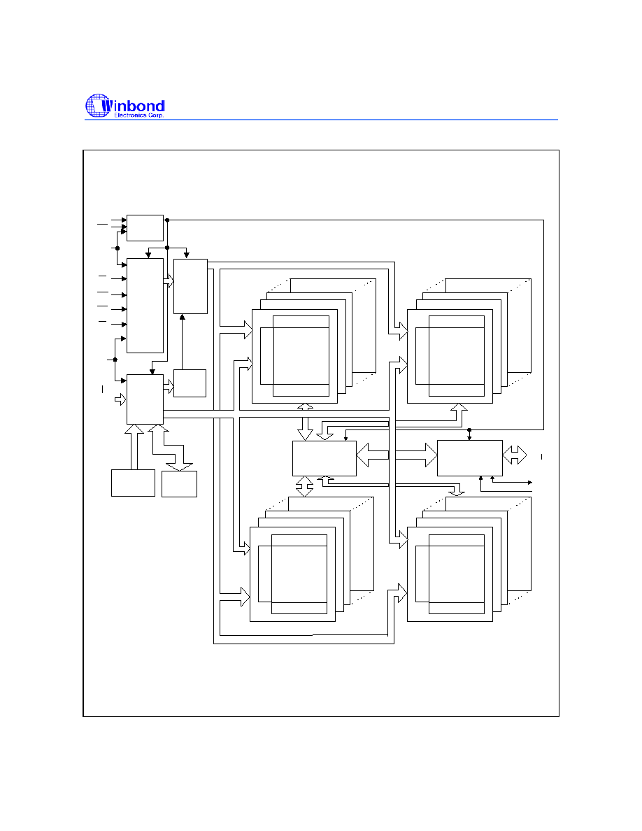
6. BLOCK DIAGRAM
CKE
A10
DLL
CLOCK
BUFFER
COMMAND
DECODER
ADDRESS
BUFFER
REFRESH
COUNTER
COLUMN
COUNTER
CONTROL
SIGNAL
GENERATOR
MODE
REGISTER
COLUMN DECODER
SENSE AMPLIFIER
CELL ARRAY
BANK #2
COLUMN DECODER
SENSE AMPLIFIER
CELL ARRAY
BANK #0
COLUMN DECODER
SENSE AMPLIFIER
CELL ARRAY
BANK #3
DATA CONTROL
CIRCUIT
DQ
BUFFER
COLUMN DECODER
SENSE AMPLIFIER
CELL ARRAY
BANK #1
NOTE:
The cell array configuration is 8912 * 512 * 16
ROW DECODER
ROW DECODER
ROW DECODER
ROW DECODER
A0
A9
A11
A12
BA0
BA1
CS
RAS
CAS
WE
CLK
CLK
DQ0
DQ15
PREFETCH REGISTER
LDM
UDM
UDQS
LDQS
W942516CH
- 8 -
7. ELECRICAL CHARACTERISTICS
7.1 Absolute Maximum Ratings
PARAMETER SYMBOL
RATING
UNIT
Input/Output Voltage
V
IN,
V
OUT
-0.3
- V
DDQ
+0.3
V
Power Supply Voltage
V
DD,
V
DDQ
-0.3
- 3.6
V
Operating Temperature
T
OPR
0
- 70
�C
Storage Temperature
T
STG
-55
- 150
�C
Soldering Temperature (10s)
T
SOLDER
260
�C
Power Dissipation
P
D
1 W
Short Circuit Output Current
I
OUT
50 mA
Note: Exposure to conditions beyond those listed under Absolute Maximum Ratings may adversely affect the life and reliability
of the device.
7.2 Recommended DC Operating Conditions
(T
A
= 0 to 70
�
C)
SYMBOL PARAMETER
MIN.
TYP.
MAX.
UNIT
NOTES
V
DD
Power Supply Voltage
2.3
2.5
2.7
V
2
V
DDQ
Power Supply Voltage (for I/O
Buffer)
2.3 2.5 V
DD
V 2
V
REF
Input reference Voltage
0.49 x V
DDQ
0.50 x V
DDQ
0.51 x V
DDQ
V 2,
3
V
TT
Termination Voltage (System)
V
REF
- 0.04
VREF
V
REF
+ 0.04
V
2, 8
V
IH (DC)
Input High Voltage (DC)
V
REF
+ 0.15
-
V
DDQ
+ 0.3
V
2
V
IL (DC)
Input Low Voltage (DC)
-0.3
-
V
REF
- 0.15
V
2
V
ICK (DC)
Differential Clock DC Input Voltage
-0.3
-
V
DDQ
+ 0.3
V
15
V
ID (DC)
Input Differential Voltage.
CLK and CLK inputs (DC)
0.36 -
V
DDQ
+ 0.6
V
13, 15
V
IH (AC)
Input High Voltage (AC)
V
REF
+ 0.31
-
-
V
2
V
IL (AC)
Input Low Voltage (AC)
-
-
V
REF
- 0.31
V
2
V
ID (AC)
Input Differential Voltage.
CLK and CLK inputs (AC)
0.7 -
V
DDQ
+ 0.6
V
13, 15
V
X (AC)
Differential AC input Cross Point
Voltage
V
DDQ
/2 - 0.2
-
V
DDQ
/2 + 0.2
V
12, 15
V
ISO (AC)
Differential Clock AC Middle Point
V
DDQ
/2 - 0.2
-
V
DDQ
/2 + 0.2
V
14, 15
Notes: Undershoot Limit: V
IL
(min) = -0.9V with a pulse width < 5 nS
Overshoot Limit: V
IH
(max) = V
DD
Q +0.9V with a pulse width < 5 nS
V
IH (DC)
and V
IL (DC)
are levels to maintain the current logic state.
V
IH (AC)
and V
IL (AC)
are levels to change to the new logic state.
W942516CH
Publication Release Date: May 20, 2003
- 9 -
Revision A2
7.3 Capacitance
(V
DD
= V
DDQ
= 2.5V
�
0.2V, f = 1 MHz, T
A
= 25
�
C, V
OUT (DC)
= V
DDQ
/2, V
OUT
(Peak to Peak) = 0.2V)
SYMBOL PARAMETER
MIN.
MAX.
DELTA
(MAX.)
UNIT
C
IN
Input Capacitance (except for CLK pins)
2.0
3.0
0.5
pF
C
CLK
Input Capacitance (CLK pins) 2.0
3.0
0.25
pF
C
I/O
DQ, DQS, DM Capacitance 4.0
5.0
0.5
pF
C
NC1
NC1 Pin Capacitance
-
1.5
-
pF
C
NC2
NC2 Pin Capacitance
4.0
5.0
-
pF
Notes: These parameters are periodically sampled and not 100% tested.
The NC2 pins have additional capacitance for adjustment of the adjacent pin capacitance.
The NC2 pins have Power and Ground clamp.
7.4 Leakage and Output Buffer Characteristics
SYMBOL PARAMETER
MIN.
MAX.
UNITS
NOTES
I
I (L)
Input Leakage Current
(0V < V
IN
< V
DDQ
, All other pins not under test = 0V)
-2 2
�A
I
O (L)
Output Leakage Current
(Output disabled, 0V < V
OUT
< V
DDQ
)
-5 5
�A
V
OH
Output High Voltage
(under AC test load condition)
V
TT
+0.76
-
V
V
OL
Output Low Voltage
(under AC test load condition)
- V
TT
-0.76
V
I
OH (DC)
Output Minimum Source DC Current -15.2
-
mA
4,
6
I
OL (DC)
Output Minimum Sink DC Current
Full
Strength
15.2 -
mA
4,
6
I
OH (DC)
Output Minimum Source DC Current
-10.4
-
mA
5
I
OL (DC)
Output Minimum Sink DC Current
Half
Strength
10.4 -
mA
5
W942516CH
- 10 -
7.5 DC
Characteristics
MAX.
SYM. PARAMETER
-5
-6
-7
-75
UNIT NOTES
I
DD0
OPERATING CURRENT: One Bank Active-Precharge; t
RC
=
t
RC
min; t
CK
= t
CK
min; DQ, DM and DQS inputs changing twice
per clock cycle; Address and control inputs changing once per
clock cycle
110 110 110 110
7
I
DD1
OPERATING CURRENT: One Bank Active-Read-Precharge;
Burst = 2; t
RC
= t
RC
min; CL = 2.5; t
CK
= t
CK
min; I
OUT
= 0 mA;
Address and control inputs changing once per clock cycle.
120 120 120 120
7,
9
I
DD2P
PRECHARGE-POWER-DOWN STANDBY CURRENT: All
Banks Idle; Power down mode; CKE < V
IL
max; t
CK
= t
CK
min;
Vin = V
REF
for DQ, DQS and DM
2 2 2 2
I
DD2F
IDLE FLOATING STANDBY CURRENT: CS > V
IH
min; All
Banks Idle; CKE > V
IH
min; Address and other control inputs
changing once per clock cycle; Vin = Vref for DQ, DQS and DM
45 45 45 40
7
I
DD2N
IDLE STANDBY CURRENT: CS > V
IH
min; All Banks Idle;
CKE > V
IH
min; t
CK
= t
CK
min; Address and other control inputs
changing once per clock cycle; Vin > V
IH
min or Vin < V
IL
max
for DQ, DQS and DM
45 45 45 40
7
I
DD2Q
IDLE QUIET STANDBY CURRENT: CS > V
IH
min; All Banks
Idle; CKE > V
IH
min; t
CK
= t
CK
min; Address and other control
inputs stable; Vin > V
REF
for DQ, DQS and DM
40 40 40 35 mA
7
I
DD3P
ACTIVE POWER-DOWN STANDBY CURRENT: One Bank
Active; Power down mode; CKE < V
IL
max; t
CK
= t
CK
min
20 20 20 20
I
DD3N
ACTIVE STANDBY CURRENT: CS > V
IH
min; CKE > V
IH
min; One Bank Active-Precharge; t
RC
= t
RAS
max; t
CK
= t
CK
min;
DQ, DM and DQS inputs changing twice per clock cycle;
Address and other control inputs changing once per clock cycle
70 70 70 65
7
I
DD4R
OPERATING CURRENT: Burst = 2; Reads; Continuous burst;
One Bank Active; Address and control inputs changing once
per clock cycle; CL=2.5; t
CK
= t
CK
min; I
OUT
= 0mA
165 165 165 155
7,
9
I
DD4
W
OPERATING CURRENT: Burst = 2; Write; Continuous burst;
One Bank Active; Address and control inputs changing once
per clock cycle; CL = 2.5; t
CK
= t
CK
min; DQ, DM and DQS
inputs changing twice per clock cycle
165 165 165 155
7
I
DD5
AUTO REFRESH CURRENT: t
RC
= t
RFC
min
190 190 190 190
7
I
DD6
SELF REFRESH CURRENT: CKE <
0.2V
3 3 3 3
I
DD7
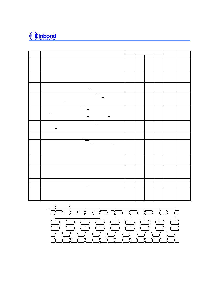
RANDOM READ CURRENT: 4 Banks Active Read with
activate every 20ns, Auto-Precharge Read every 20 nS; Burst
= 4; t
RCD
= 3; I
OUT
= 0mA; DQ, DM and DQS inputs changing
twice per clock cycle; Address changing once per clock cycle
270 270 270 270
CK
CK
DQS
RANDOM READ CURRENT Timing
t
RCD
t
RC
t
CK = 10ns
(
I
DD7)
Bank 0
Row d
Bank 3
Row c
Bank 1
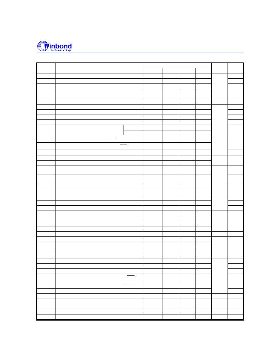
Row e
Bank 1
Row e
ADDRESS
Bank 0
Row d
Bank 2
Row f
Bank 3
Row q
Bank 2
Col f
READ
AP
ACT
READ
AP
COMMAND
READ
AP
ACT
ACT
READ
AP
ACT
DQ
Qa
Qb
Qb
Qb
Qb
Qc
Qc
Qc
Qc
Qd
Qd
Qd
Qd
Qe
Qe
Qa
Bank 0
Row h
ACT
Bank 0
Col d
READ
AP
ACT
ACT
ACT
ACT
Bank 1
Col e
Bank 2
Row f
Bank 3
Row q
Bank 2
Col f
Bank 0
Row h
READ
AP
Bank 1
Row e
Bank 3
Col c
Bank 0
Row d
W942516CH
Publication Release Date: May 20, 2003
- 11 -
Revision A2
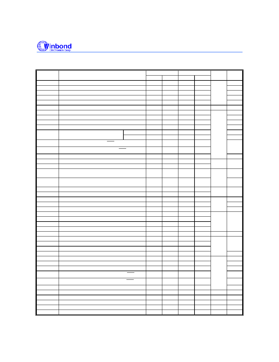
7.6 AC Characteristics and Operating Condition
(Notes: 10, 12)
-7 -75
SYMBOL PARAMETER
MIN. MAX. MIN. MAX.
UNITS NOTES
t
RC
Active to Ref/Active Command Period
65
65
t
RFC
Ref to Ref/Active Command Period
75
75
t
RAS
Active to Precharge Command Period
45
100000
45 100000
t
RCD
Active to Read/Write Command Delay Time
20
20
t
RAP
Active to Read with Auto Precharge Enable
15
15
nS
t
CCD
Read/Write(a) to Read/Write(b) Command Period
1
1
t
CK
t
RP
Precharge to Active Command Period
20
20
t
RRD
Active(a) to Active(b) Command Period
15
15
t
WR
Write Recovery Time
15
15
t
DAL
Auto Precharge Write Recovery + Precharge Time
30
30
CL = 2
7.5
15
8
15
t
CK
CLK Cycle Time
CL = 2.5
7
15
7.5
15
t
AC
Data Access Time from CLK, CLK
-0.75 0.75 -0.75 0.75
t
DQSCK
DQS Output Access Time from CLK, CLK
-0.75 0.75 -0.75 0.75
16
t
DQSQ
Data Strobe Edge to Output Data Edge Skew
0.5
0.5
nS
t
CH
CLk High Level Width
0.45
0.55
0.45
0.55
t
CL
CLK Low Level Width
0.45
0.55
0.45
0.55
t
CK
11
t
HP
CLK Half Period (minimum of actual t
CH,
t
CL
)
Min.
(t
CL
,t
CH
)
Min.
(t
CL
,t
CH
)
t
QH
DQ Output Data Hold Time from DQS
T
HP
-0.75
T
HP
-0.75
nS
t
RPRE
DQS Read Preamble Time
0.9
1.1
0.9
1.1
t
RPST
DQS Read Postamble Time
0.4
0.6
0.4
0.6
t
CK
11
t
DS
DQ and DM Setup Time
0.5
0.5
t
DH
DQ and DM Hold Time
0.5
0.5
t
DIPW
DQ and DM Input Pulse Width (for each input)
1.75
1.75
nS
t
DQSH
DQS Input High Pulse Width
0.35
0.35
t
DQSL
DQS Input Low Pulse Width
0.35
0.35
t
DSS
DQS Falling Edge to CLK Setup Time
0.2
0.2
t
DSH
DQS Falling Edge Hold Time from CLK
0.2
0.2
t
CK
11
t
WPRES
Clock to DQS Write Preamble Set-up Time
0
0
nS
t
WPRE
DQS Write Preamble Time
0.25
0.25
t
WPST
DQS Write Postamble Time
0.4
0.4
t
DQSS
Write Command to First DQS Latching Transition
0.75
1.25
0.75
1.25
11
t
DSSK
UDQS � LDQS Skew (x 16)
-0.25
0.25
-0.25
0.25
t
CK
t
IS
Input Setup Time
0.9
0.9
t
IH
Input Hold Time
0.9
0.9
t
IPW
Control & Address Input Pulse Width (for each input)
2.2
2.2
t
HZ
Data-out High-impedance Time from CLK, CLK
-0.75 0.75 -0.75 0.75
t
LZ
Data-out Low-impedance Time from CLK, CLK
-0.75 0.75 -0.75 0.75
t
T(SS)
SSTL Input Transition
0.5
1.5
0.5
1.5
nS
t
WTR
Internal Write to Read Command Delay
1
1
t
CK
t
XSNR
Exit Self Refresh to non-Read Command
75
75
ns
t
XSRD
Exit Self Refresh to Read Command
10
10
t
CK
t
REF
Refresh Time (8k)
64
64
mS
t
MRD
Mode Register Set Cycle Time
15
15
nS
W942516CH
- 12 -
-5 -6
SYM. PARAMETER
MIN. MAX. MIN. MAX.
UNITS NOTES
t
RC
Active to Ref/Active Command Period
55
60
t
RFC
Ref to Ref/Active Command Period
70
72
t
RAS
Active to Precharge Command Period
40
70000
42
100000
t
RCD
Active to Read/Write Command Delay Time
15
18
t
RAP
Active to Read with Auto Precharge Enable
15
15
nS
t
CCD
Read/Write(a) to Read/Write(b) Command Period
1
1
tCK
t
RP
Precharge to Active Command Period
15
18
t
RRD
Active(a) to Active(b) Command Period
10
12
t
WR
Write Recovery Time
15
15
t
DAL
Auto Precharge Write Recovery + Precharge Time
30
30
2.5 5 10 6 12
t
CK
CLK Cycle Time
3
5 10 6 12
t
AC
Data Access Time from CLK, CLK
-0.7 0.7 -0.7 0.7
t
DQSCK
DQS Output Access Time from CLK, CLK
-0.55 0.55 -0.6 0.6
16
t
DQSQ
Data Strobe Edge to Output Data Edge Skew
0.4
0.45
nS
t
CH
CLk High Level Width
0.45
0.55
0.45
0.55
t
CL
CLK Low Level Width
0.45
0.55
0.45
0.55
tCK 11
t
HP
CLK Half Period (minimum of actual t
CH,
t
CL
)
Min.
(tCL,tCH)
Min.
(tCL,tCH)
t
QH
DQ Output Data Hold Time from DQS
tHP
-0.5
tHP
-0.55
nS
t
RPRE
DQS Read Preamble Time
0.9
1.1
0.9
1.1
t
RPST
DQS Read Postamble Time
0.4
0.6
0.4
0.6
tCK 11
t
DS
DQ and DM Setup Time
0.4
0.45
t
DH
DQ and DM Hold Time
0.4
0.45
t
DIPW
DQ and DM Input Pulse Width (for each input)
1.75
1.75
nS
t
DQSH
DQS Input High Pulse Width
0.35
0.35
t
DQSL
DQS Input Low Pulse Width
0.35
0.35
t
DSS
DQS Falling Edge to CLK Setup Time
0.2
0.2
t
DSH
DQS Falling Edge Hold Time from CLK
0.2
0.2
tCK 11
t
WPRES
Clock to DQS Write Preamble Set-up Time
0
0
nS
t
WPRE
DQS Write Preamble Time
0.25
0.25
t
WPST
DQS Write Postamble Time
0.4
0.6
0.4
0.6
t
DQSS
Write Command to First DQS Latching
Transition 0.72 1.28 0.75 1.25
11
t
DSSK
UDQS � LDQS Skew (x 16)
-0.25
0.25
-0.25
0.25
tCK
t
IS
Input
Setup
Time
0.6
0.75
t
IH
Input
Hold
Time
0.6
0.75
t
IPW
Control & Address Input Pulse Width (for each input)
2.2
2.2
t
HZ
Data-out High-impedance Time from CLK, CLK
Max
tAC
-0.7 0.7
t
LZ
Data-out Low-impedance Time from CLK, CLK
-0.7 0.7 -0.7 0.7
t
T(SS)
SSTL
Input
Transition
0.5 1.5 0.5 1.5
nS
t
WTR
Internal Write to Read Command Delay
2
2
tCK
t
XSNR
Exit Self Refresh to non-Read Command
75
75
ns
t
XSRD
Exit Self Refresh to Read Command
10
10
tCK
t
REF
Refresh
Time
(8k)
64 64
mS
t
MRD
Mode Register Set Cycle Time
10
12
nS
W942516CH
Publication Release Date: May 20, 2003
- 13 -
Revision A2
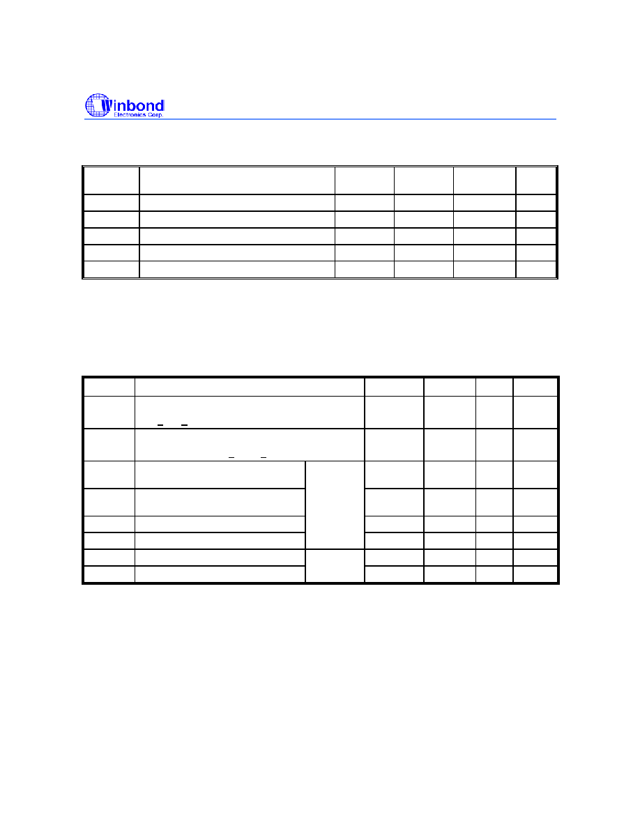
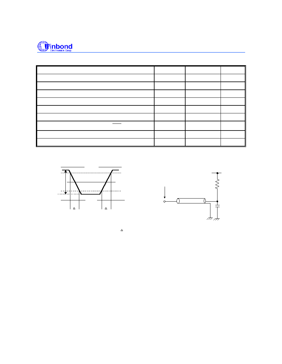
7.7 AC Test Conditions
PARAMETER SYMBOL
VALUE
UNIT
Input High Voltage (AC)
V
IH
V
REF
+0.31
V
Input Low Voltage (AC)
V
IL
V
REF
-0.31
V
Input Reference Voltage
V
REF
0.5 x V
DDQ
V
Termination Voltage
V
TT
0.5 x V
DDQ
V
Input Signal Peak to Peak Swing
V
SWING
1.0 V
Differential Clock Input Reference Voltage
V
R
V
x
(AC) V
Input Difference Voltage. CLK and
CLK
Inputs (AC)
V
ID (AC)
1.5 V
Input Signal Minimum Slew Rate
SLEW
1.0
V/nS
Output Timing Measurement Reference Voltage
V
OTR
0.5 x V
DDQ
V
V
SWING (MAX)
V
DD
Q
V
SS
T
T
V
IH
min (AC)
V
REF
V
IL
max (AC)
SLEW = (V
IH
min (AC) - V
IL
max (AC)) /
T
Output
R
T
= 50 ohms
VTT
A.C. TEST LOAD (A)
Z = 50 ohms
output
30pF
Measurement point
Notes:
(1)
Conditions outside the limits listed under "ABSOLUTE MAXIMUM RATINGS" may cause permanent damage to the
device.
(2)
All voltages are referenced to V
SS
, V
SSQ. .(
2.6V
�
0.1V for DDR400
)
(3)
Peak to peak AC noise on V
REF
may not exceed
�
2% V
REF(DC).
(4) V
OH
= 1.95V, V
OL
= 0.35V
(5) V
OH
= 1.9V, V
OL
= 0.4V
(6)
The values of I
OH(DC)
is based on V
DDQ
= 2.3V and V
TT
= 1.19V.
The values of I
OL(DC)
is based on V
DDQ
= 2.3V and V
TT
= 1.11V.
(7)
These parameters depend on the cycle rate and these values are measured at a cycle rate with the minimum values
of t
CK
and t
RC
.
(8) V
TT
is not applied directly to the device. V
TT
is a system supply for signal termination resistors, is expected to be set
equal to V
REF
and must track variations in the DC level of V
REF
.
(9)
These parameters depend on the output loading. Specified values are obtained with the output open.
W942516CH
- 14 -
(10) Transition times are measured between V
IH
min(AC)
and V
IL
max(AC)
.Transition (rise and fall) of input signals have a fixed
slope.
(11) IF the result of nominal calculation with regard to t
CK
contains more than one decimal place, the result is rounded up to
the nearest decimal place.
(i.e., T
DQSS
= 0.75
�
t
CK
, t
CK
= 7.5 nS, 0.75
�
7.5 nS = 5.625 nS is rounded up to 5.6 nS.)
(12) V
X
is the differential clock cross point voltage where input timing measurement is referenced.
(13) V
ID
is magnitude of the difference between CLK input level and CLK input level.
(14) V
ISO
means {V
ICK
(CLK)+V
( CLK )}/2.
ICK
(15) Refer to the figure below.
CLK
CLK
V
SS
V
ICK
V
X
V
X
V
X
V
X
V
X
V
ICK
V
ICK
V
ICK
V
ID(AC)
V
ID(AC)
0 V Differential
V
ISO
V
ISO(min)
V
ISO(max)
V
SS
(16) t
AC
and t
DQSCK
depend on the clock jitter. These timing are measured at stable clock.
W942516CH
Publication Release Date: May 20, 2003
- 15 -
Revision A2
8. OPERATION MODE
The following table shows the operation commands.
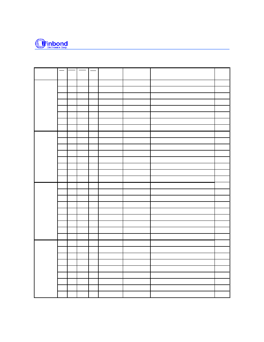
8.1 Simplified Truth Table
SYM. COMMAND
DEVICE
STATE
CKEN-1
CKEN
DM
(4)
BS0,
BS1
A10
A12,
A11,
A9-A0
CS
RAS
CAS
WE
ACT Bank
Active
Idle
(3)
H X X V V V L
L H
H
PRE Bank
Precharge Any
(3)
H X X V L X L
L H
L
PREA Precharge
All
Any
H
X X X H X L L H L
WRIT Write
Active
(3)
H X X V L V L
H L L
WRITA
Write with Auto
Precharge
Active
(3)
H X X V H V L H L L
READ Read
Active
(3)
H X X V L V L H L H
READA
Read with Auto
Precharge
Active
(3)
H X X V H V L H L H
MRS
Mode Register
Set
Idle H X
X
L,
L
C C
L
L
L
L
EMRS
Extended Mode
Regiser Set
Idle H X
X
H,
L
V V
L
L
L
L
NOP No
Operation
Any H X X X X X L H H H
BST
Burst Read Stop
Active
H
X
X
X
X
X
L
H
H
L
DSL Device
Deselect Any H X X X X X H X X X
AREF
Auto
Refresh
Idle H H X X X X L
L L H
SELF
Self Refresh
Entry
Idle H L X
X
X X
L
L
L
H
H X X X
SELEX
Self Refresh Exit
Idle
(Self
Refresh)
L H X X X X
L H
H
X
H X X X
PD
Power Down
Dode Entry
Idle/
Active
(5)
H L X X
X X
L H
H
X
H X X X
PDEX
Power Down
Mode Exit
Any
(Power
Down)
L H X X X X
L H
H
X
WDE
Data Write
Enable
Active H X L X X X X
X X X
WDD
Data Write
Disable
Active H X H X X X X
X X X
Notes
:
1. V = Valid X = Don't Care L = Low level H = High level
2.
CKE
n
signal is input level when commands are issued.
CKE
n-1
signal is input level one clock cycle before the commands are issued.
4. These are state designated by the BS0, BS1 signals.
5. LDM, UDM (W942516CH)
6. Power Down Mode can not entry in the burst cycle.
W942516CH
- 16 -
8.2 Function Truth Table
(Note 1)
CURRENT
STATE
CS
RAS
CAS
WE
ADDRESS COMMAND
ACTION
NOTES
H X X X X
DSL
Nop
L H H X X
NOP/BST
Nop
L
H
L
H
BS, CA, A10
READ/READA
ILLEGAL
3
L
H
L
L
BS, CA, A10
WRIT/WRITA
ILLEGAL
3
L L H H BS,
RA
ACT
Row
activating
L L H L BS,
A10
PRE/PREA Nop
L
L
L
H
X
AREF/SELF
Refresh or Self refresh
2
Idle
L L L L Op-Code MRS/EMRS Mode
register
accessing
2
H X X X X
DSL
Nop
L H H X X
NOP/BST
Nop
L
H
L
H
BS, CA, A10
READ/READA
Begin read: Determine AP
4
L
H
L
L
BS, CA, A10
WRIT/WRITA
Begin write: Determine AP
4
L L H H BS,
RA
ACT
ILLEGAL
3
L L H L BS,
A10
PRE/PREA Precharge
5
L L L H X
AREF/SELF ILLEGAL
Row Active
L L L L Op-Code MRS/EMRS ILLEGAL
H
X
X
X
X
DSL
Continue burst to end
L
H
H
H
X
NOP
Continue burst to end
L H H L X
BST
Burst
stop
L
H
L
H
BS, CA, A10
READ/READA
Term burst, new read: Determine AP
6
L
H
L
L
BS, CA, A10
WRIT/WRITA
ILLEGAL
L L H H BS,
RA
ACT
ILLEGAL
3
L
L
H
L
BS, A10
PRE/PREA
Term burst, precharging
L L L H X
AREF/SELF ILLEGAL
Read
L L L L Op-Code MRS/EMRS ILLEGAL
H
X
X
X
X
DSL
Continue burst to end
L
H
H
H
X
NOP
Continue burst to end
L H H L X
BST
ILLEGAL
L
H
L
H
BS, CA, A10
READ/READA
Term burst, start read: Determine AP
6, 7
L
H
L
L
BS, CA, A10
WRIT/WRITA
Term burst, start read: Determine AP
6
L L H H BS,
RA
ACT
ILLEGAL
3
L
L
H
L
BS, A10
PRE/PREA
Term burst. precharging
8
L L L H X
AREF/SELF ILLEGAL
Write
L L L L Op-Code MRS/EMRS ILLEGAL
W942516CH
Publication Release Date: May 20, 2003
- 17 -
Revision A2
Function Truth Table, continued
CURRENT
STATE
CS
RAS
CAS
WE
ADDRESS COMMAND
ACTION
NOTES
H
X
X
X
X
DSL
Continue burst to end
L
H
H
H
X
NOP
Continue burst to end
L H H L X
BST
ILLEGAL
L
H
L
H
BS, CA, A10 READ/READA
ILLEGAL
L
H
L
L
BS, CA, A10 WRIT/WRITA
ILLEGAL
3
L L H H BS,
RA
ACT
ILLEGAL
3
L L H L BS,
A10 PRE/PREA
ILLEGAL
L L L H X
AREF/SELF
ILLEGAL
Read with
Auto
Prechange
L L L L Op-Code MRS/EMRS
ILLEGAL
H
X
X
X
X
DSL
Continue burst to end
L
H
H
H
X
NOP
Continue burst to end
L H H L X
BST
ILLEGAL
L
H
L
H
BS, CA, A10 READ/READA
ILLEGAL
L
H
L
L
BS, CA, A10 WRIT/WRITA
ILLEGAL
L L H H BS,
RA
ACT
ILLEGAL
3
L L H L BS,
A10 PRE/PREA
ILLEGAL
3
L L L H X
AREF/SELF
ILLEGAL
Write with
Auto
Precharge
L L L L Op-Code MRS/EMRS
ILLEGAL
H X X X X
DSL
Nop
->
Idle after t
RP
L H H H X
NOP
Nop
->
Idle after t
RP
L H H L X
BST
ILLEGAL
L
H
L
H
BS, CA, A10 READ/READA
ILLEGAL
3
L
H
L
L
BS, CA, A10 WRIT/WRITA
ILLEGAL
3
L L H H BS,
RA
ACT
ILLEGAL
3
L
L
H
L
BS, A10
PRE/PREA
Idle after t
RP
L L L H X
AREF/SELF
ILLEGAL
Precharging
L L L L Op-Code MRS/EMRS
ILLEGAL
H X X X X
DSL
Nop
->
Row active after t
RCD
L H H H X
NOP
Nop
->
Row active after t
RCD
L H H L X
BST
ILLEGAL
L
H
L
H
BS, CA, A10 READ/READA
ILLEGAL
3
L
H
L
L
BS, CA, A10 WRIT/WRITA
ILLEGAL
3
L L H H BS,
RA
ACT
ILLEGAL
3
L L H L BS,
A10 PRE/PREA
ILLEGAL
3
L L L H X
AREF/SELF
ILLEGAL
Row
Activating
L L L L Op-Code MRS/EMRS
ILLEGAL
W942516CH
- 18 -
Function Truth Table, continued
CURRENT
STATE
CS RAS
CAS
WE
ADDRESS COMMAND
ACTION
NOTES
H X X X X
DSL
Nop
->
Row active after t
WR
L H H H X
NOP
Nop
->
Row active after t
WR
L H H L X
BST
ILLEGAL
L
H
L
H
BS, CA, A10
READ/READA
ILLEGAL
3
L
H
L
L
BS, CA, A10
WRIT/WRITA
ILLEGAL
3
L L H H BS,
RA
ACT
ILLEGAL
3
L L H L BS,
A10
PRE/PREA
ILLEGAL
3
L L L H X
AREF/SELF
ILLEGAL
Write
Recovering
L L L L Op-Code MRS/EMRS
ILLEGAL
H X X X X
DSL
Nop
->
Enter precharge after t
WR
L H H H X
NOP
Nop
->
Enter precharge after t
WR
L H H L X
BST
ILLEGAL
L
H
L
H
BS, CA, A10
READ/READA
ILLEGAL
3
L
H
L
L
BS, CA, A10
WRIT/WRITA
ILLEGAL
3
L L H H BS,
RA
ACT
ILLEGAL
3
L L H L BS,
A10
PRE/PREA
ILLEGAL
3
L L L H X
AREF/SELF
ILLEGAL
Write
Recovering
with Auto
Precharge
L L L L Op-Code MRS/EMRS
ILLEGAL
H X X X X
DSL
Nop
->
Idle after t
RC
L H H H X
NOP
Nop
->
Idle after t
RC
L H H L X
BST
ILLEGAL
L H L H X
READ/WRIT
ILLEGAL
L L H X X
ACT/PRE/PREA
ILLEGAL
Refreshing
L L L X X
AREF/SELF/MRS/EMRS
ILLEGAL
H X X X X
DSL
Nop
->
Row after t
MRD
L H H H X
NOP
Nop
->
Row after t
MRD
L H H L X
BST
ILLEGAL
L H L X X
READ/WRIT
ILLEGAL
Mode
Register
Accessing
L L X X X
ACT/PRE/PREA/ARE
F/SELF/MRS/EMRS
ILLEGAL
Notes
:
1. All entries assume that CKE was active (High level) during the preceding clock cycle and the current clock cycle.
2. Illegal if any bank is not idle.
3. Illegal to bank in specified states; Function may be legal in the bank indicated by Bank Address (BS), depending on the
state of that bank.
4. Illegal if t
RCD
is not satisfied.
5. Illegal if t
RAS
is not satisfied.
6. Must satisfy burst interrupt condition.
7. Must avoid bus contention, bus turn around, and/or satisfy write recovery requirements.
8. Must mask preceding data which don't satisfy t
WR
Remark: H = High level, L = Low level, X = High or Low level (Don't care), V = Valid data
W942516CH
Publication Release Date: May 20, 2003
- 19 -
Revision A2
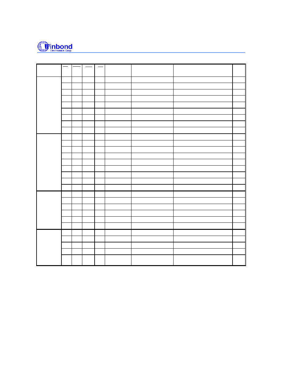
8.3 Function Truth Table for CKE
CKE
CURRENT
STATE
n-1 n
CS
ADDRESS ACTION NOTES
H X X X X X
X
INVALID
L
H
H
X
X
X
X
Exit Self Refresh
->
Idle after t
XSNR
L
H
L
H
H
X
X
Exit Self Refresh
->
Idle after t
XSNR
L H L H L X
X
ILLEGAL
L H L L X X
X
ILLEGAL
Self Refresh
L L X X X X
X
Maintain
Self
Refresh
H X X X X X
X
INVALID
L
H
X
X
X
X
X
Exit Power down
->
Idle after t
IS
Power Down
L
L
X
X
X
X
X
Maintain power down mode
H
H
X
X
X
X
X
Refer to Function Truth Table
H L H X X X
X
Enter
Power
down
2
H L L H H X
X
Enter
Power
down
2
H L L L L H
X
Self
Refresh
1
H L L H L X
X
ILLEGAL
H L L L X X
X
ILLEGAL
All banks Idle
L X X X X X
X
Power
down
2
H
H
X
X
X
X
X
Refer to Function Truth Table
H L H X X X
X
Enter
Power
down
2
H L L H H X
X
Enter
Power
down
2
H L L L L H
X
ILLEGAL
H L L H L X
X
ILLEGAL
H L L L X X
X
ILLEGAL
Row Active
L X X X X X
X
Power
down
Any State
Other Than
Listed Above
H
H
X
X
X
X
X
Refer to Function Truth Table
RAS
CAS
WE
Notes
:
1. Self refresh can enter only from the all banks idle state.
2. Power down can enter only from bank idle or row active state.
Remark: H = High level, L = Low level, X = High or Low level (Don't care), V = Valid data
W942516CH
- 20 -
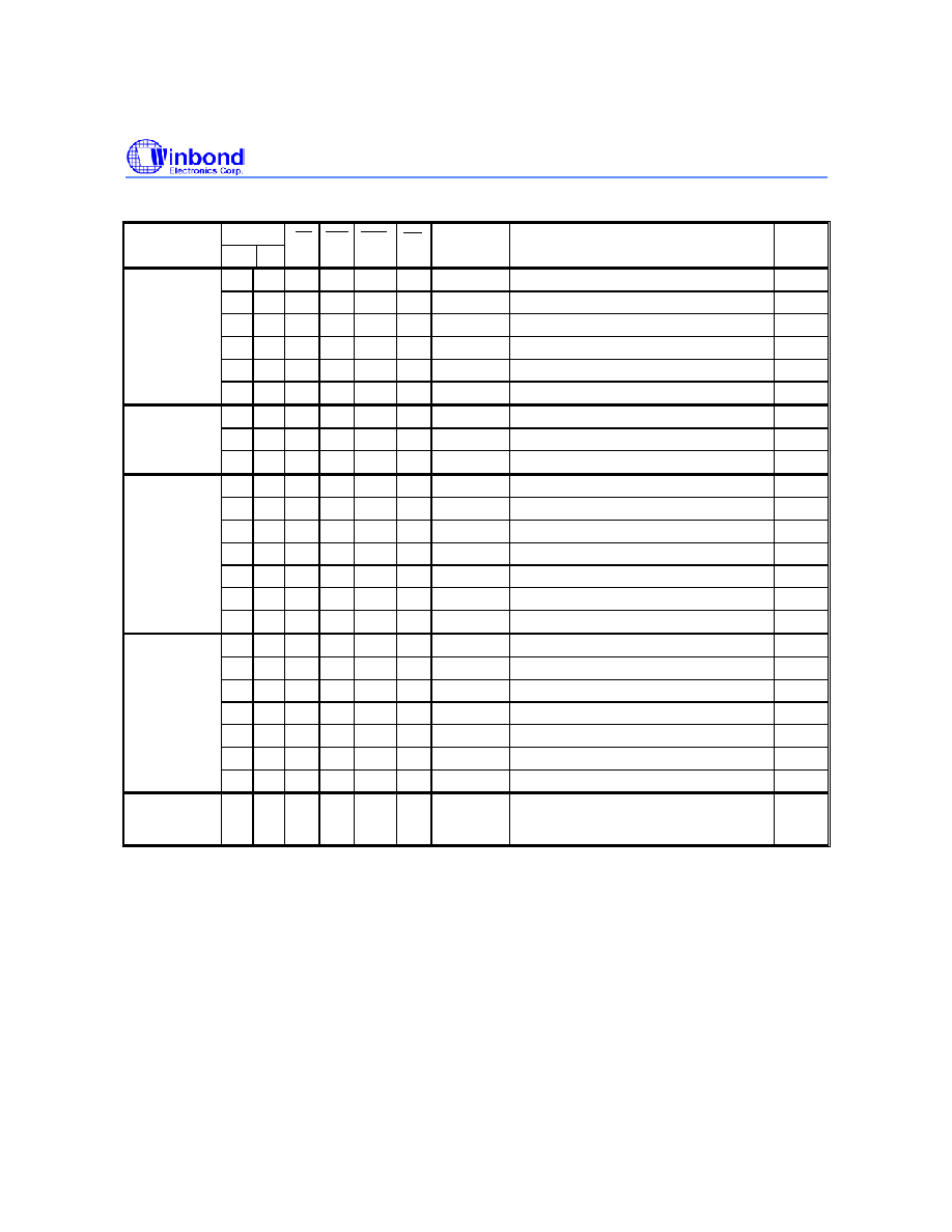
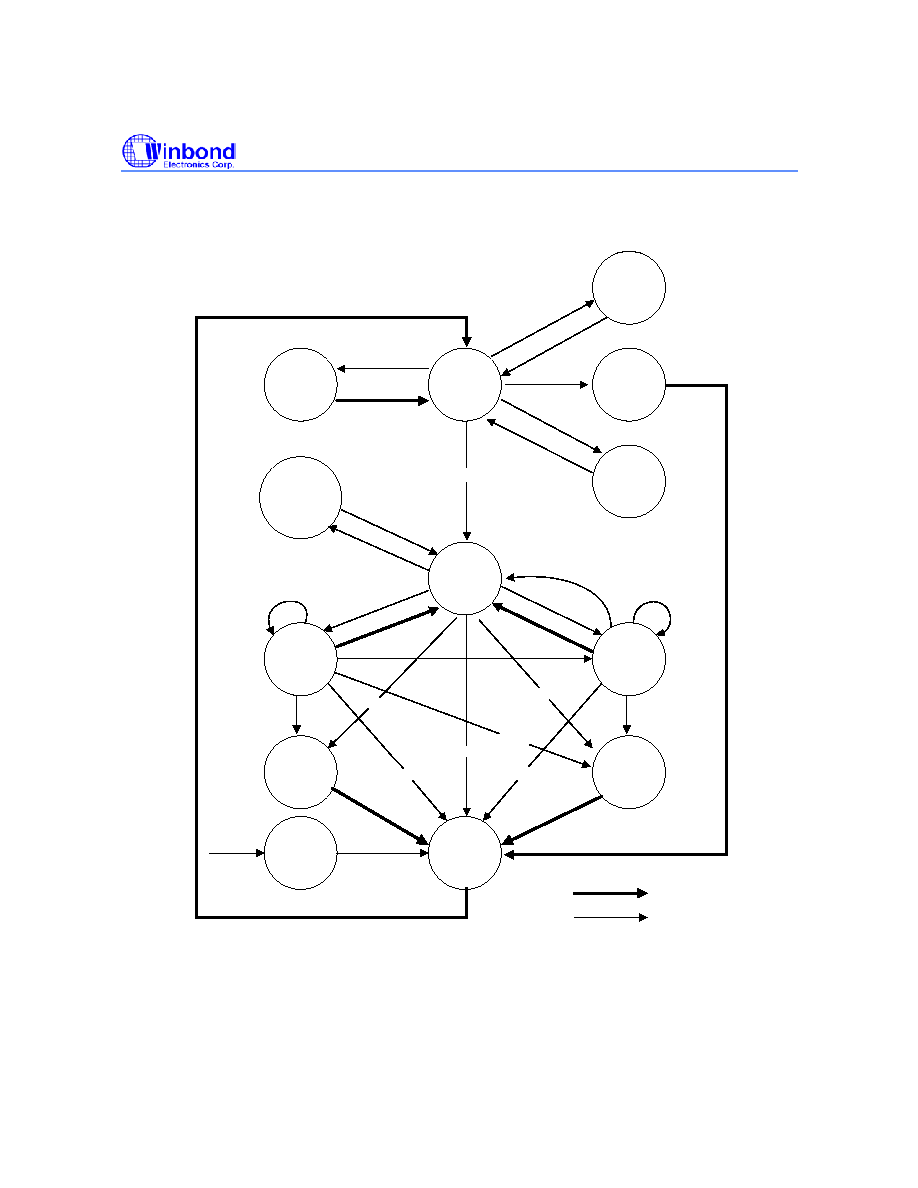
8.4 Simplified Stated Diagram
POWER
APPLIED
Automatic Sequence
Command Sequence
Read A
Write
Read
ROW
ACTIVE
POWER
DOWN
IDLE
MODE
REGISTER
SET
AUTO
REFRESH
SELF
REFRESH
Read
Read A
Write
Write A
PRE
CHARGE
POWER
ON
MRS/EMRS
AREF
SREF
SREFX
PD
PDEX
ACT
BST
Read
Write
Write A
Write A
Read A
PRE
PRE
PRE
PRE
ACTIVE
POWERDOWN
PD
PDEX
Read
Read A

W942516CH
Publication Release Date: May 20, 2003
- 21 -
Revision A2
9. FUNCTIONAL DESCRIPTION
9.1 Power Up Sequence
(1) Apply power and attempt to CKE at a low state (
0.2V), all other inputs may be undefined
1) Apply V
DD
before or at the same time as V
DDQ
.
2) Apply V
DDQ
before or at the same time as V
TT
and V
REF
.
(2) Start Clock and maintain stable condition for 200
�S (min.).
(3) After stable power and clock, apply NOP and take CKE high.
(4) Issue EMRS (Extended Mode Register Set) to enable DLL and establish Output Driver Type.
(5) Issue MRS (Mode Register Set) to reset DLL and set device to idle with bit A8.
(an additional 200 cycles(min) of clock are required for DLL Lock)
(6) Issue precharge command for all banks of the device.
(7) Issue two or more Auto Refresh commands.
(8) Issue MRS-Initialize device operation.
(If device operation mode is set at sequence 5, sequence 8 can be skipped.)
9.2 Command
Function
1. Bank Activate Command
(
RAS
= "L",
CAS
= "H",
WE
= "H", BS0, BS1 = Bank, A0 to A12 = Row Address)
The Bank Activate command activates the bank designated by the BS (Bank address) signal. Row
addresses are latched on A0 to A12 when this command is issued and the cell data is read out of
the sense amplifiers. The maximum time that each bank can be held in the active state is specified
as t
RAS (max)
. After this command is issued, Read or Write operation can be executed.
2. Bank Precharge Command
(
RAS
= "L",
CAS
= "H",
WE
= "L", BS0, BS1 = Bank, A10 = "L", A0 to A9, A11, A12 = Don't
care)
The Bank Precharge command percharges the bank designated by BS. The precharged bank is
switched from the active state to the idle state.
3. Precharge All Command
(
RAS
= "L",
CAS
= "H",
WE
= "L", BS0, BS1 = Don't care, A10 = "H", A0 to A9, A11, A12 =
Don't care)
The Precharge All command precharges all banks simultaneously. Then all banks are switched to
the idle state.
4. Write Command
(
RAS
= "H",
CAS
= "L",
WE
= "L", BS0, BS1 = Bank, A10 = "L", A0 to A9, A11 = Column
Address)

W942516CH
- 22 -
The write command performs a Write operation to the bank designated by BS. The write data are
latched at both edges of DQS. The length of the write data (Burst Length) and column access
sequence (Addressing Mode) must be in the Mode Register at power-up prior to the Write
operation.
5. Write with Auto Precharge Command
(
RAS
= "H",
CAS
= "L",
WE
= "L", BS0, BS1 = Bank, A10 = "H", A0 to A9, A11 = Column
Address)
The Write with Auto Precharge command performs the Precharge operation automatically after the
Write operation. This command must not be interrupted by any other commands.
6. Read Command
(
RAS
= "H",
CAS
= "L",
WE
= "H", BS0, BS1 = Bank, A10 = "L", A0 to A9, A11 = Column
Address)
The Read command performs a Read operation to the bank designated by BS. The read data are
synchronized with both edges of DQS. The length of read data (Burst Length), Addressing Mode
and
CAS
Latency (access time from
CAS
command in a clock cycle) must be programmed in
the Mode Register at power-up prior to the Read operation.
7. Read with Auto Precharge Command
(
RAS
= "H",
CAS
= "L",
WE
= "H", BS0, BS1 = Bank, A10 = "H", A0 to A9, A11 = Column
Address)
The Read with Auto precharge command automatically performs the Precharge operation after the
Read operation.
1) READA
t
RAS (min)
- (BL/2) x t
CK
Internal precharge operation begins after BL/2 cycle from Read with Auto Precharge command.
2) t
RCD(min)
READA < t
RAS(min)
- (BL/2) x t
CK
Data can be read with shortest latency, but the internal Precharge operation does not begin until
after t
RAS (min)
has completed.
This command must not be interrupted by any other command.
8. Mode Register Set Command
(
RAS
= "L",
CAS
= "L",
WE
= "L", BS0 = "L", BS1 = "L", A0 to A12 = Register Data)
The Mode Register Set command programs the values of
CAS
latency, Addressing Mode, Burst
Length and DLL reset in the Mode Register. The default values in the Mode Register after power-
up are undefined, therefore this command must be issued during the power-up sequence. Also,
this command can be issued while all banks are in the idle state. Refer to the table for specific
codes.
9. Extended Mode Register Set Command
(
RAS
= "L",
CAS
= "L",
WE
= "L", BS0 = "H", BS1 = "L", A0 to A12 = Register data)

W942516CH
Publication Release Date: May 20, 2003
- 23 -
Revision A2
The Extended Mode Register Set command can be implemented as needed for function
extensions to the standard (SDR-SDRAM). Currently the only available mode in EMRS is DLL
enable/disable, decoded by A0. The default value of the extended mode register is not defined;
therefore this command must be issued during the power-up sequence for enabling DLL. Refer to
the table for specific codes.
10. No-Operation Command
(
RAS
= "H",
CAS
= "H",
WE
= "H")
The No-Operation command simply performs no operation (same command as Device Deselect).
11. Burst Read Stop Command
(
RAS
= "H",
CAS
= "H",
WE
= "L")
The Burst stop command is used to stop the burst operation. This command is only valid during a
Burst Read operation.
12. Device Deselect Command
(
CS
= "H")
The Device Deselect command disables the command decoder so that the
RAS
,
CAS
,
WE
and Address inputs are ignored. This command is similar to the No-Operation command.
13. Auto Refresh Command
(
RAS
= "L",
CAS
= "L",
WE
= "H", CKE = "L", BS0, BS1, A0 to A12 = Don't care)
The Auto Refresh command is used to refresh the row address provided by the internal refresh
counter. The Refresh operation must be performed 8192 times within 64ms. The next command
can be issued after t
REF
from the end of the Auto Refresh command. When the Auto Refresh
command is used, all banks must be in the idle state.
14. Self Refresh Entry Command
(
RAS
= "L",
CAS
= "L",
WE
= "H", CKE = "L", BS0, BS1, A0 to A12 = don't care)
The Self Refresh Entry command is used to enter Self Refresh mode. While the device is in Self
Refresh mode, all input and output buffer (except the CKE buffer) are disabled and the Refresh
operation is automatically performed. Self Refresh mode is exited by taking CKE "high" (the Self
Refresh Exit command). During self refresh, DLLl is disable.
15. Self Refresh Exit Command
(CKE = "H",
CS
= "H" or CKE = "H",
RAS
= "H",
CAS
= "H")
This command is used to exit from Self Refresh mode. Any subsequent commands can be issued
after t
XSNR
(t
XSRD
for Read Command) from the end of this command.

W942516CH
- 24 -
16. Data Write Enable /Disable Command
(DM = "L/H" or LDM, UDM = "L/H")
During a Write cycle, the DM or LDM, UDM signal functions as Data Mask and can control every
word of the input data. The LDM signal controls DQ0 to DQ7 and UDM signal controls DQ8 to
DQ15.
9.3 Read
Operation
Issuing the Bank Activate command to the idle bank puts it into the active state. When the Read
command is issued after t
RCD
from the Bank Activate command, the data is read out sequentially,
synchronized with both edges of DQS (Burst Read operation). The initial read data becomes available
after
CAS
latency from the issuing of the Read command. The
CAS
latency must be set in the Mode
Register at power-up.
When the Precharge Operation is performed on a bank during a Burst Read and operation, the Burst
operation is terminated.
When the Read with Auto Precharge command is issued, the Precharge operation is performed
automatically after the Read cycle, then the bank is switched to the idle state. This command cannot
be interrupted by any other commands. Refer to the diagrams for Read operation.
9.4 Write
Operation
Issuing the Write command after t
RCD
from the bank activate command. The input data is latched
sequentially, synchronizing with both edges(rising &falling) of DQS after the Write command (Burst
write operation). The burst length of the Write data (Burst Length) and Addressing Mode must be set
in the Mode Register at power-up.
When the Precharge operation is performed in a bank during a Burst Write operation, the Burst
operation is terminated.
When the Write with Auto Precharge command is issued, the Precharge operation is performed
automatically after the Write cycle, then the bank is switched to the idle state, The Write with Auto
Precharge command cannot be interrupted by any other command for the entire burst data duration.
Refer to the diagrams for Write operation.
9.5 Precharge
There are two Commands, which perform the precharge operation (Bank Precharge and Precharge
All). When the Bank Precharge command is issued to the active bank, the bank is precharged and
then switched to the idle state. The Bank Precharge command can precharge one bank independently
of the other bank and hold the unprecharged bank in the active state. The maximum time each bank
can be held in the active state is specified as t
RAS (max)
. Therefore, each bank must be precharged
within t
RAS(max)
from the bank activate command.
The Precharge All command can be used to precharge all banks simultaneously. Even if banks are
not in the active state, the Precharge All command can still be issued. In this case, the Precharge
operation is performed only for the active bank and the precharge bank is then switched to the idle
state.

W942516CH
Publication Release Date: May 20, 2003
- 25 -
Revision A2
9.6 Burst
Termination
When the Precharge command is used for a bank in a Burst cycle, the Burst operation is terminated.
When Burst Read cycle is interrupted by the Precharge command, read operation is disabled after
clock cycle of (
CAS
latency) from the Precharge command. When the Burst Write cycle is interrupted
by the Precharge command . the input circuit is reset at the same clock cycle at which the precharge
command is issued. In this case, the DM signal must be asserted "high": during t
WR
to prevent writing
the invalided data to the cell array.
When the Burst Read Stop command is issued for the bank in a Burst Read cycle, the Burst Read
operation is terminated. The Burst read Stop command is not supported during a write burst operation.
Refer to the diagrams for Burst termination.
9.7 Refresh
Operation
Two types of Refresh operation can be performed on the device: Auto Refresh and Self Refresh. By
repeating the Auto Refresh cycle, each bank in turn refreshed automatically. The Refresh operation
must be performed 8192 times(rows)within 64ms. The period between the Auto Refresh command
and the next command is specified by t
RFC
.
Self Refresh mode enter issuing the Self Refresh command (CKE asserted "low"). while all banks are
in the idle state. The device is in Self Refresh mode for as long as cke held "low". In the case of
8192 burst Auto Refresh commands, 8192 burst Auto Refresh commands must be performed within
7.8
�S before entering and after exiting the Self Refresh mode. In the case of distributed Auto Refresh
commands, distributed auto refresh commands must be issued every 7.8
�S and the last distributed
Auto Refresh commands must be performed within 7.8
�S before entering the self refresh mode. After
exiting from the Self Refresh mode, the refresh operation must be performed within 7.8
�S. In Self
Refresh mode, all input/output buffers are disable, resulting in lower power dissipation (except CKE
buffer). Refer to the diagrams for Refresh operation.
9.8 Power Down Mode
Two types of Power Down Mode can be performed on the device: Active Standby Power Down Mode
and Precharge Standby Power Down Mode.
When the device enters the Power Down Mode, all input/output buffers and DLL are disabled resulting
in low power dissipation (except CKE buffer).
Power Down Mode enter asserting CKE "low" while the device is not running a burst cycle. Taking
CKE: "high" can exit this mode. When CKE goes high, a No operation command must be input at next
CLK rising edge. Refer to the diagrams for Power Down Mode.
9.9 Mode Register Operation
The mode register is programmed by the Mode Register Set command (MRS/EMRS) when all banks
are in the idle state. The data to be set in the Mode Register is transferred using the A0 to A12 and
BS0, BS1 address inputs.
The Mode Register designates the operation mode for the read or write cycle. The register is divided
into five filed: (1) Burst Length field to set the length of burst data (2) Addressing Mode selected bit to
designate the column access sequence in a Burst cycle (3)
CAS
Latency field to set the assess time
in clock cycle (4) DLL reset field to reset the dll (5) Regular/Extended Mode Register filed to select a
W942516CH
- 26 -
type of MRS (Regular/Extended MRS). EMRS cycle can be implemented the extended function (DLL
enable/Disable mode)
The initial value of the Mode Register (including EMRS) after power up is undefined; therefore the
Mode Register Set command must be issued before power operation.
1. Burst Length field (A2 to A0)
This field specifies the data length for column access using the A2 to A0 pins and sets the Burst
Length to be 2, 4, and 8 words.
A2 A1 A0 Burst
Length
0 0 0 Reserved
0 0 1 2
words
0 1 0 4
words
0 1 1 8
words
1 x x Reserved
2. Addressing Mode Select (A3)
The Addressing Mode can be one of two modes; Interleave mode or Sequential Mode, When the
A3 bit is "0", Sequential mode is selected. When the A3 bit is "1", Interleave mode is selected. Both
addressing Mode support burst length 2, 4, and 8 words.
A3 Addressing
Mode
0 Sequential
0 Interleave
W942516CH
Publication Release Date: May 20, 2003
- 27 -
Revision A2
� Address Sequence of Sequential Mode
A column access is performed by incrementing the column address input to the device. The
address is varied by the Burst Length as the following.
Addressing Sequence of Sequential Mode
DATA
ACCESS ADDRESS
BURST LENGTH
Data 0
n
2 words (address bits is A0)
Data 1
n + 1
not carried from A0 to A1
Data 2
n + 2
4 words (address bit A0, A1)
Data 3
n + 3
Not carried from A1 to A2
Data 4
n + 4
Data 5
n + 5
8 words (address bits A2, A1 and A0)
Data 6
n + 6
Not carried from A2 to A3
Data 7
n + 7
� Addressing Sequence of Interleave Mode
A Column access is started from the inputted column address and is performed by
interleaving the address bits in the sequence shown as the following.
9.9.1.1 Address Sequence for Interleave Mode
DATA
ACCESS ADDRESS
BURST LENGTH
Data 0
A8 A7 A6 A5 A4 A3 A2 A1 A0
2 words
Data 1
A8 A7 A6 A5 A4 A3 A2 A1
A0
Data 2
A8 A7 A6 A5 A4 A3 A2
A1
A0
4 words
Data 3
A8 A7 A6 A5 A4 A3 A2
A1
A0
Data 4
A8 A7 A6 A5 A4 A3
A2
A1 A0
8 words
Data 5
A8 A7 A6 A5 A4 A3
A2
A1
A0
Data 6
A8 A7 A6 A5 A4 A3
A2
A1
A0
Data 7
A8 A7 A6 A5 A4 A3
A2
A1
A0
W942516CH
- 28 -
3.
CAS
Latency field (A6 to A4)
This field specifies the number of clock cycles from the assertion of the Read command to the first
data read. The minimum values of
CAS
Latency depends on the frequency of CLK.
A6 A5 A4
CAS Latency
0 0 0
Reserved
0 0 1
Reserved
0 1 0
2
0 1 1
3
1 0 0
Reserved
1 0 1
Reserved
1 1 0
2.5
1 1 1
Reserved
4. DLL Reset bit (A8)
This bit is used to reset DLL. When the A8 bit is "1", DLL is reset.
5. Mode Register /Extended Mode register change bits (BS0, BS1)
These bits are used to select MRS/EMRS.
BS1 BS0
A12-A0
0
0
Regular MRS Cycle
0
1
Extended MRS Cycle
1 x
Reserved
6. Extended Mode Register field
1) DLL Switch field (A0)
This bit is used to select DLL enable or disable
A0 DLL
0 Enable
1 Disable
2) Output Driver Size Control field (A1)
This bit is used to select Output Driver Size, both Full strength and Half strength are based on
JEDEC standard.
A1 Output
Driver
0 Full
Strength
1 Half
Strength
7. Reserved field
� Test mode entry bit (A7)
This bit is used to enter Test mode and must be set to "0" for normal operation.
� Reserved bits (A9, A10, A11, A12)
These bits are reserved for future operations. They must be set to "0" for normal operation.
W942516CH
Publication Release Date: May 20, 2003
- 29 -
Revision A2
10. TIMING WAVEFORMS
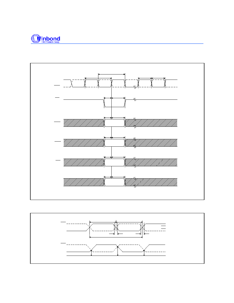
10.1 Command Input Timing
CLK
CLK
t
CK
t
CK
t
CL
t
CH
t
IS
t
IH
t
IS
t
IH
t
IS
t
IH
t
IS
t
IH
t
IS
t
IH
CS
RAS
CAS
WE
A0~A12
BS0, 1
Refer to the Command Truth Table
10.2 Timing of the CLK Signals
t
CK
t
T
t
T
V
IH
V
IH(AC)
V
IL(AC)
V
IL
CLK
CLK
CLK
CLK
V
X
V
X
V
X
V
IH
V
IL
t
CH
t
CL
W942516CH
- 30 -
Timing Waveforms, continued
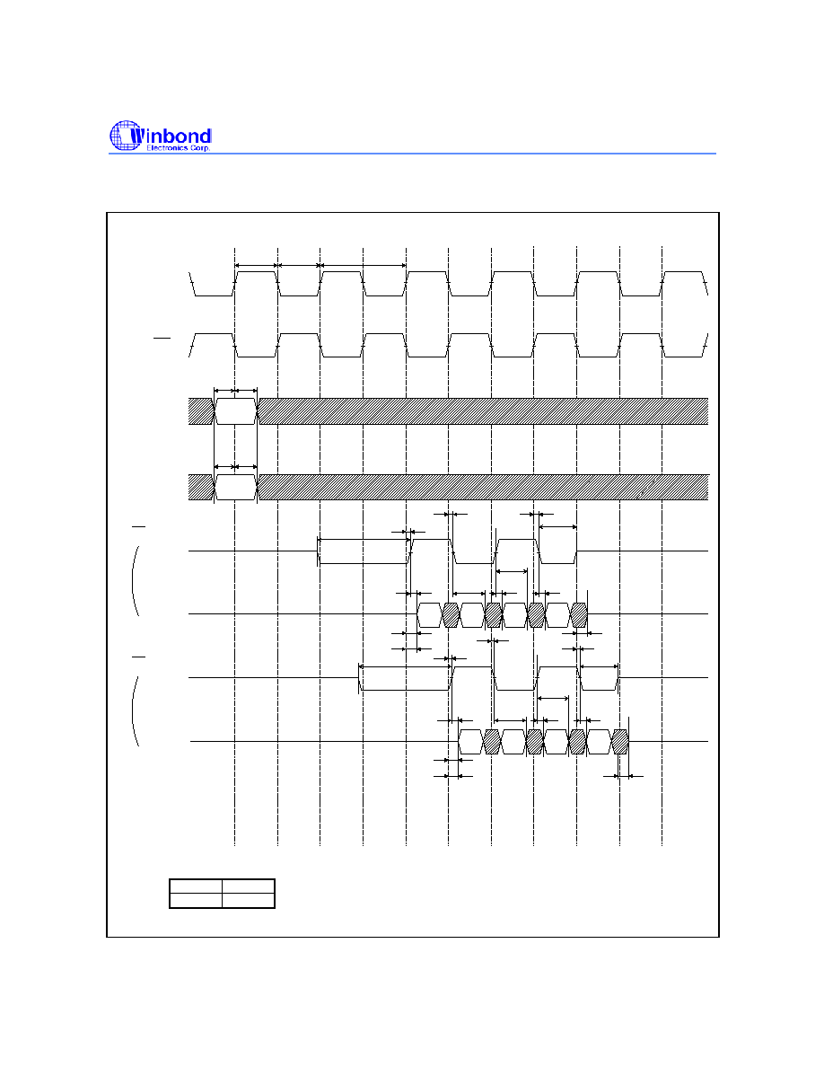
10.3 Read Timing (Burst Length = 4)
t
IS
t
IH
DA0
DA1
DA2
t
CH
t
CL
t
CK
ADD
CMD
CLK
CLK
READ
Col
QA0
QA1
QA2
DA3
QA3
t
RPRE
t
DQSCK
t
DQSCK
t
DQSCK
t
RPST
Postamble
Preamble
Hi-Z
Hi-Z
t
DQSQ
t
DQSQ
t
DQSQ
t
QH
t
QH
t
AC
t
LZ
t
HZ
Hi-Z
Hi-Z
DA0
DA1
DA2
QA0
QA1
QA2
DA3
QA3
t
RPRE
t
DQSCK
t
DQSCK
t
DQSCK
t
RPST
Postamble
Preamble
Hi-Z
Hi-Z
t
DQSQ
t
DQSQ
t
DQSQ
t
QH
t
QH
t
AC
t
LZ
t
HZ
Hi-Z
Hi-Z
CAS
DQS
Output
(Data)
latency=2
CAS
DQS
Output
(Data)
latency=2.5
Note: The correspondence of LDQS, UDQS to DQ. ( W942516AH)
LDQS
DQ0~7
DQ8~15
UDQS
t
IS
t
IH
W942516CH
Publication Release Date: May 20, 2003
- 31 -
Revision A2
Timing Waveforms, continued
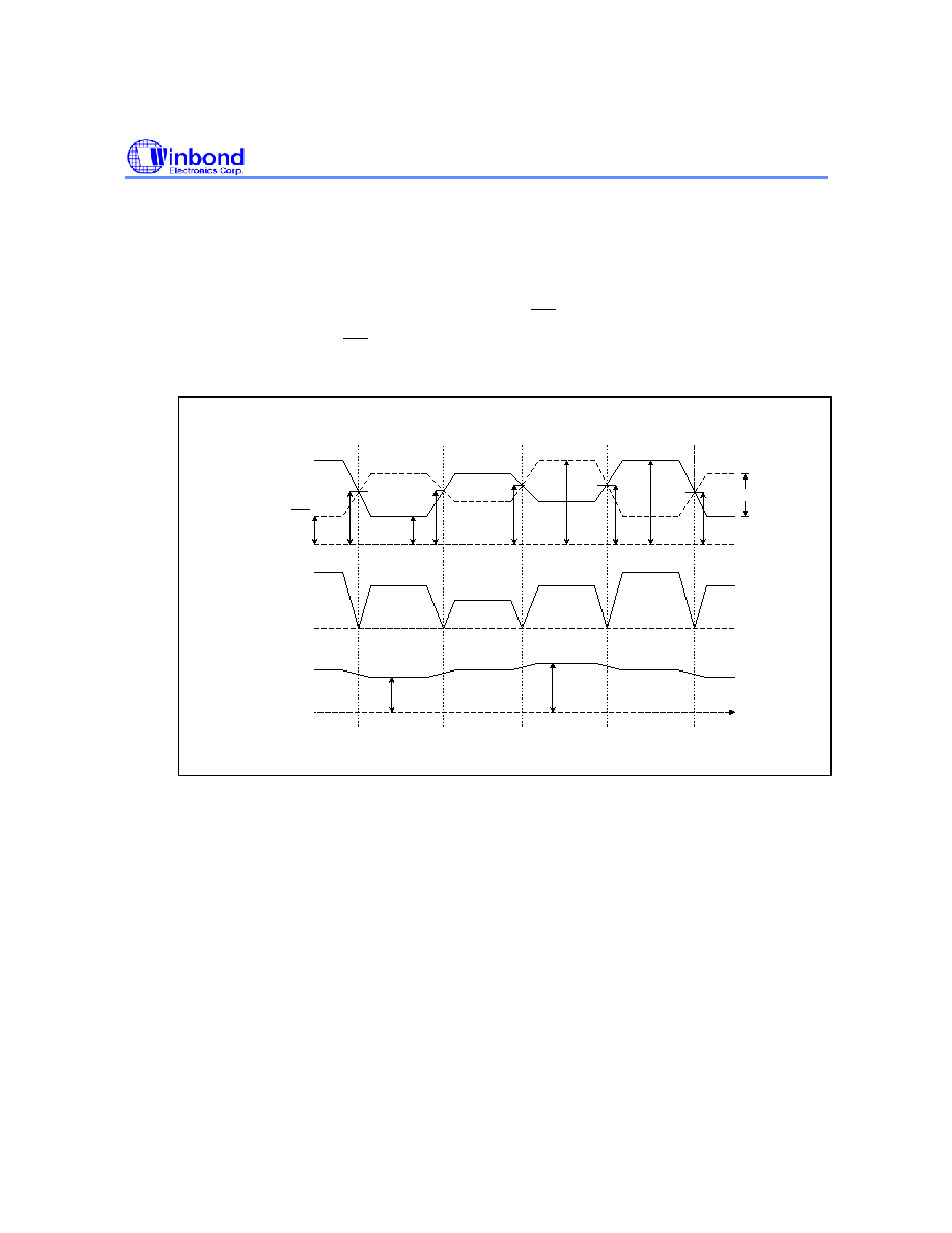
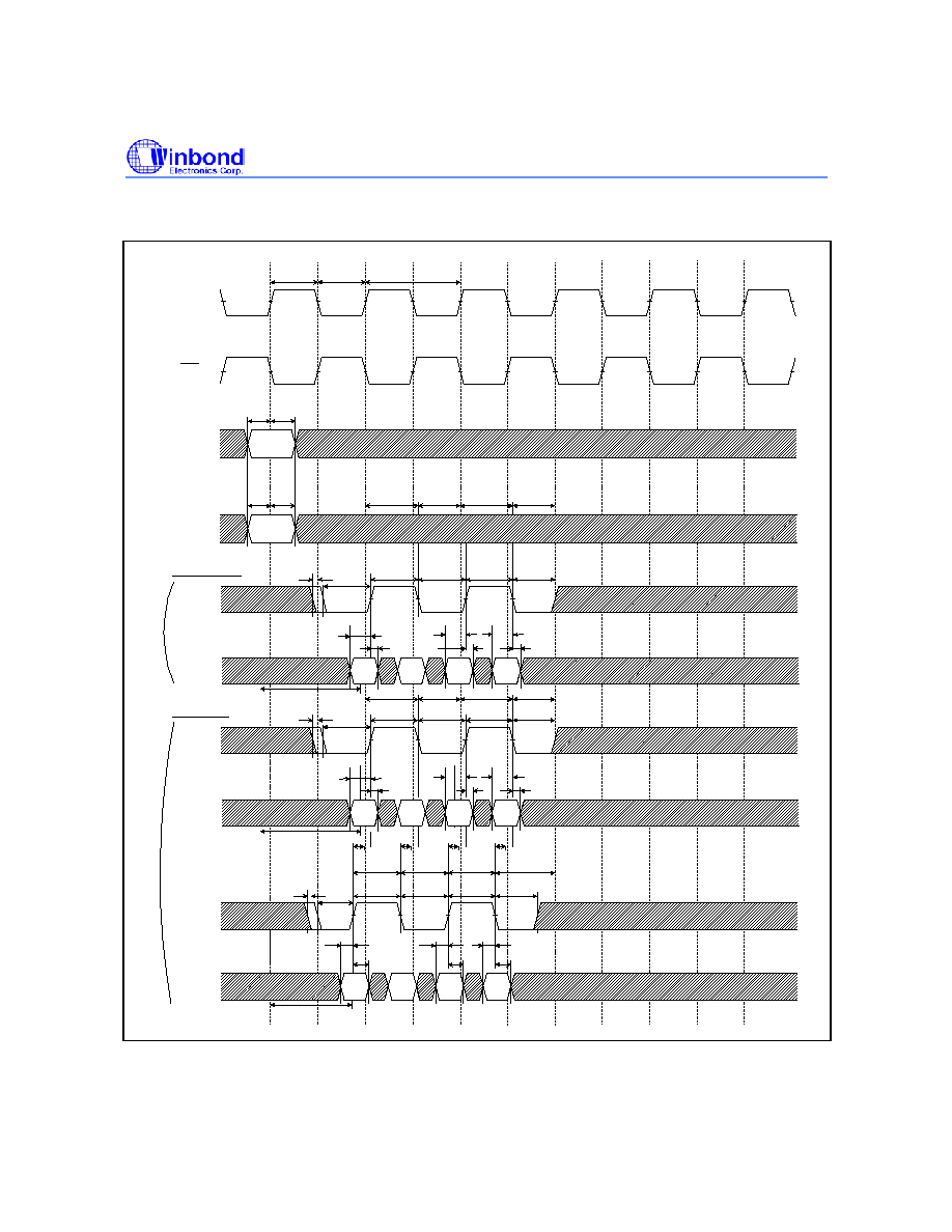
10.4 Write Timing (Burst Length = 4)
t
IS
t
IH
tDSH
t
DSS
t
DSS
t
DSH
t
WPRES
t
DH
t
DH
t
DH
t
DS
t
DS
t
DS
t
DQSS
t
DSH
t
DSH
t
DSS
t
DSS
Postamble
t
WPRE
Preamble
tDQSH
tDQSH
tDQSL
tWPST
DA0
DA1
DA2
DA3
t
WPRES
t
DS
t
DS
t
DQSS
t
DSH
t
DSH
t
DSS
t
DSS
Postamble
t
WPRE
Preamble
t
DQSH
t
DQSH
t
DQSL
t
WPST
t
WPRES
t
DH
t
DS
t
DS
t
DQSS
t
DSH
Postamble
t
WPRE
Preamble
t
DQSH
t
DQSH
t
DQSL
t
WPST
DA0
DA1
DA2
DA3
t
DSSK
t
DSSK
t
DSSK
t
DSSK
t
DS
t
DH
t
DH
t
CH
t
CL
t
CK
DQS
Input
(Data)
LDQS
DQ0~7
UDQS
DQ8~15
x4, x8 device
x16 device
ADD
CMD
CLK
CLK
WRIT
Col
DA0
DA1
DA2
DA3
DA0
DA1
DA2
DA3
t
DH
t
DH
t
DH
t
DS
DA0
DA1
DA2
DA3
DA0
DA1
DA2
DA3
Note: x16 has 2DQS's (UDQS for uper byte and LDQS for lower byte). Even if one of the 2 bytes is not used, both UDQS and
LDQS must be toggled.
W942516CH
- 32 -
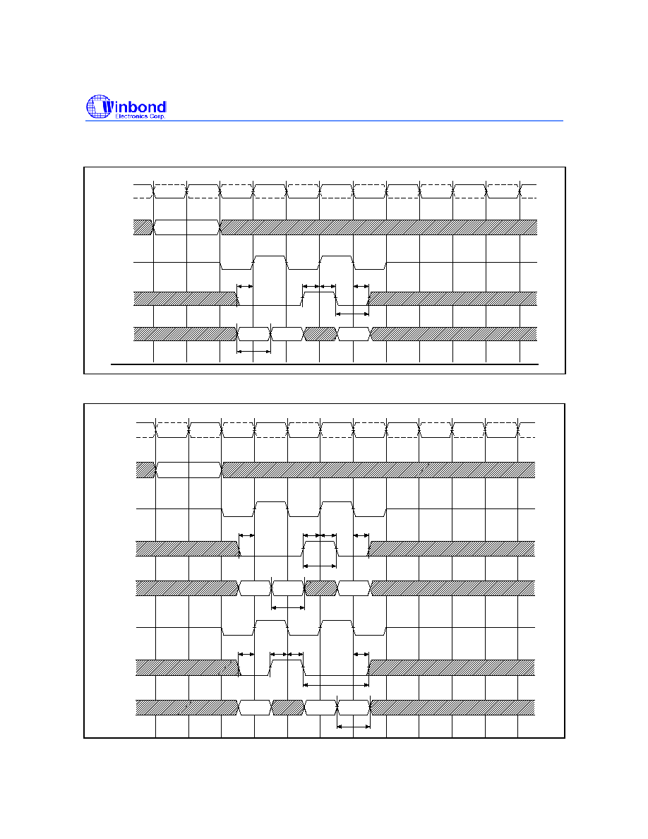
Timing Waveforms, continued
10.5 DM, Data Mask (W942508CH /W942504CH)
WRIT
t
DIPW
t
DIPW
t
DH
t
DH
t
DS
t
DS
Masked
/CLK
CLK
CMD
DQS
DM
DQ
D3
D1
D0
10.6 DM, Data Mask (W942516CH)
WRIT
t
DIPW
t
DIPW
t
DH
t
DH
t
DS
t
DS
Masked
/CLK
CLK
CMD
LDQS
LDM
DQ0~
DQ7
D3
D1
D0
t
DIPW
t
DIPW
t
DH
t
DH
t
DS
t
DS
Masked
UDQS
UDM
DQ8~
DQ15
D3
D2
D0
W942516CH
Publication Release Date: May 20, 2003
- 33 -
Revision A2
Timing Waveforms, continued
10.7 Mode Register Set (MRS) Timing
MRS
Register Set data
NEXT CMD
t
MRD
CLK
CLK
CMD
ADD
A2
A1
A0
A3
A6
A5
A4
A8
BS1
BS0
0
0
0
0
0
0
0
0
1
0
1
0
0
1
1
1
0
0
1
0
1
1
1
0
1
1
1
0
0
1
0
1
0
0
1
1
1
0
0
1
0
1
1
1
0
1
1
1
0
1
0
1
1
1
0
0
0
1
0
1
2
4
8
2
4
8
Burst Length
Sequential
Interleaved
Reserved
Reserved
Reserved
Reserved
Reserved
Reserved
Sequential
Interleaved
Addressing Mode
CAS Latency
2
DLL Reset
No
Yes
MRS or EMRS
Regular MRS cycle
Extended MRS cycle
2.5
A0
A1
A2
A3
A4
A5
A6
A7
A8
A9
A10
A11
A12
BS0
BS1
"0"
"0"
"0"
"0"
"0"
"0"
"0"
DLL Reset
Reserved
Addressing Mode
* "Reserved" should stay "0" during
MRS cycle.
Reserved
Mode Register Set or
Extended Mode Register
Set
CAS Latency
Burst Length
Reserved
Reserved
3
W942516CH
- 34 -
Timing Waveforms, continued
10.8 Extend Mode Register Set (EMRS) Timing
EMRS
Register Set data
NEXT CMD
t
MRD
CLK
CLK
CMD
ADD
A0
A1
BS1
BS0
0
1
0
1
1
1
0
0
0
1
0
1
Enable
Disable
DLL Switch
Output Driver Size
Full Strength
Hall Strength
MRS or EMRS
Regular MRS cycle
Extended MRS cycle
A0
A1
A2
A3
A4
A5
A6
A7
A8
A9
A10
A11
A12
BS0
BS1
"0"
"0"
"0"
"0"
"0"
"0"
"0"
* "Reserved" should stay "0" during
EMRS cycle.
"0"
"0"
"0"
"0"
"0"
"0"
Output Driver
DLL Switch
Reserved
Mode Register Set or
Extended Mode Register
Set
W942516CH
Publication Release Date: May 20, 2003
- 35 -
Revision A2
Timing Waveforms, continued
10.9 Auto Precharge Timing (Read Cycle, CL = 2)
1) tRCD (READA)
tRAS (min) � (BL/2) � tCK
AP
Q7
Q6
Q5
Q4
Q3
Q2
Q1
Q0
ACT
READA
ACT
Q0
Q1
Q2
Q3
ACT
READA
ACT
Q0
Q1
ACT
AP
READA
ACT
tRP
t
RAS
CMD
DQS
DQ
CMD
DQS
DQ
CMD
DQS
DQ
BL=2
BL=4
BL=8
CLK
CLK
AP
Notes: CL2 shown; same command operation timing with CL = 2.5
In this case, the internal precharge operation begin after BL/2 cycle from READA command.
AP
Represents the start of internal precharging.
The Read with Auto precharge command cannot be interrupted by any other command.
W942516CH
- 36 -
Auto Precharge Timing (Read cycle, CL = 2), continued
2) tRCD/RAP(min)
tRCD (READA) < tRAS (min) � (BL/2) � tCK
AP
Q7
Q6
Q5
Q4
Q3
Q2
Q1
Q0
ACT
READA
ACT
Q0
Q1
Q2
Q3
ACT
READA
ACT
Q0
Q1
ACT
AP
READA
ACT
t
RP
t
RAS
CMD
DQS
DQ
CMD
DQS
DQ
CMD
DQS
DQ
BL=2
BL=4
BL=8
CLK
CLK
AP
t
RAP
t
RCD
t
RAP
t
RCD
t
RAP
t
RCD
Notes: CL2 shown; same command operation timing with CL = 2.5
In this case, the internal precharge operation does not begin until after t
RAS
(min) has command.
AP
Represents the start of internal precharging.
The Read with Auto Precharge command cannot be interrupted by any other command.
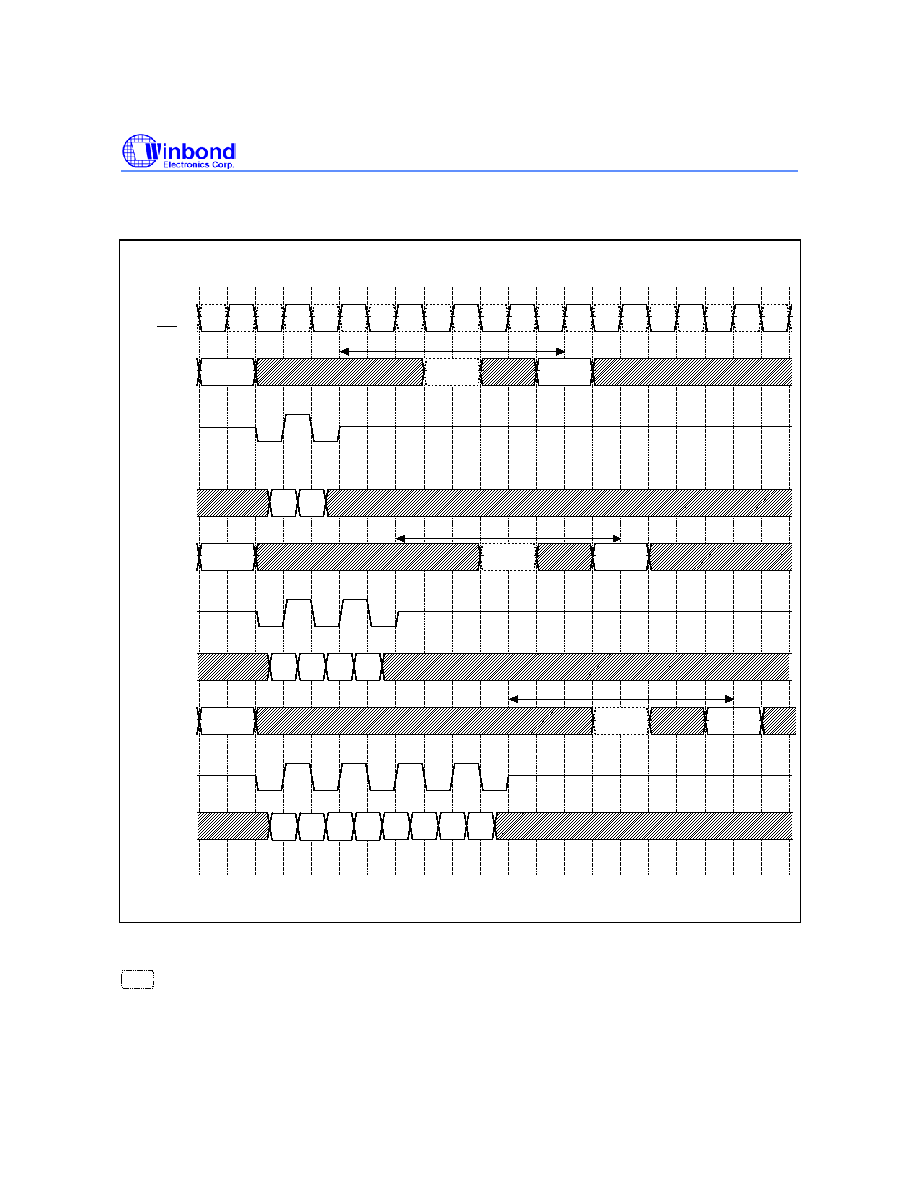
W942516CH
Publication Release Date: May 20, 2003
- 37 -
Revision A2
Timing Waveforms, continued
10.10 Auto Precharge Timing (Write Cycle)
AP
WRITA
ACT
ACT
WRITA
ACT
WRITA
CMD
DQS
DQ
CMD
DQS
DQ
CMD
DQS
DQ
BL=2
BL=4
BL=8
CLK
CLK
AP
AP
D0
D1
D0
D1
D2
D3
D0
D1
D2
D3
D4
D5
D6
D7
t
DAL
t
DAL
t
DAL
The Write with Auto Precharge command cannot be interrupted by any other command.
AP
Represents the start of internal precharging .
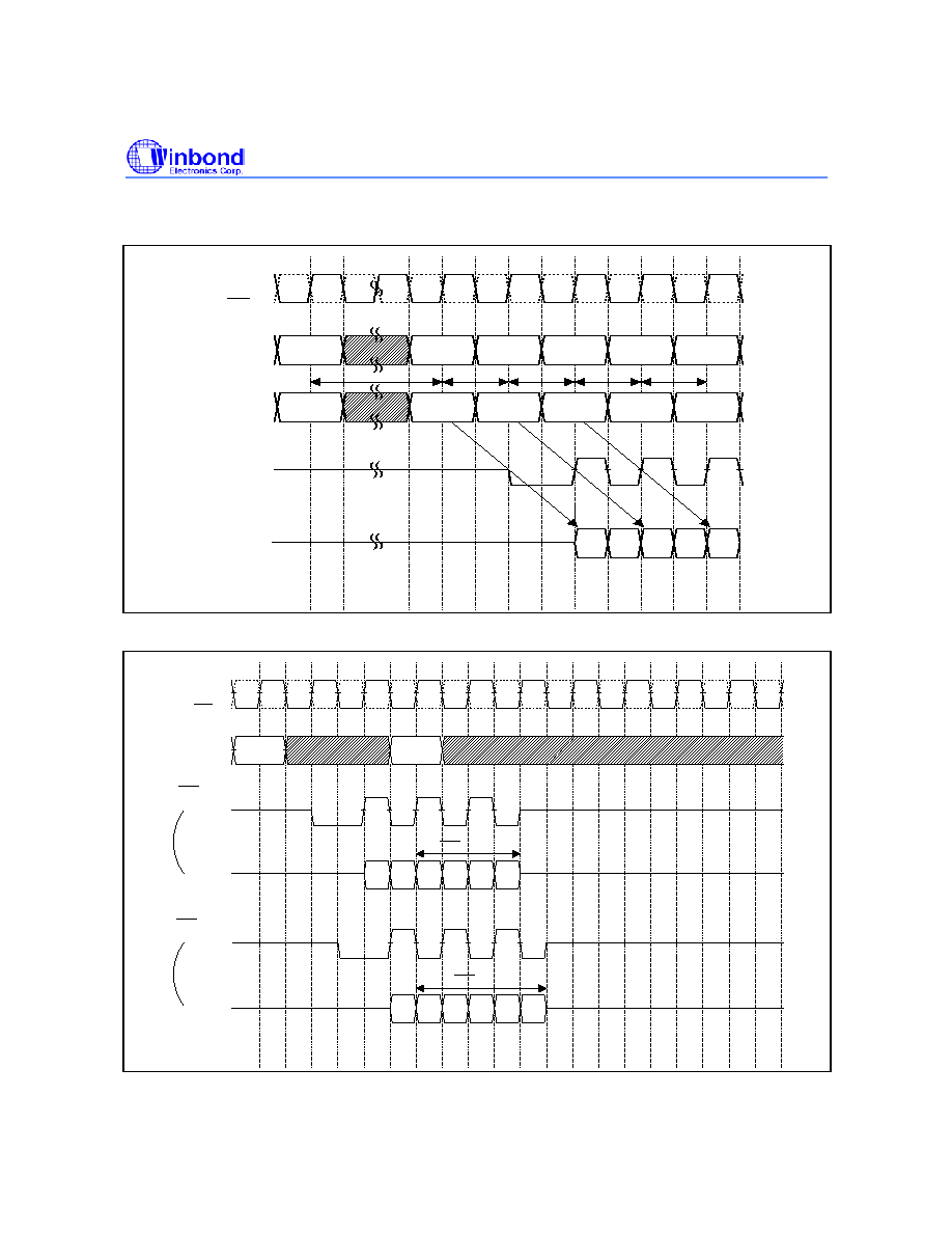
W942516CH
- 38 -
Timing Waveforms, continued
10.11 Read Interrupted by Read (CL = 2, BL = 2, 4, 8)
CMD
ADD
DQS
CLK
CLK
DQ
ACT
READ A
READ B
READ C
READ D
READ E
Row
Address
COl,Add,A
Col,Add,B
Col,Add,C
Col,Add,D
Col,Add,E
QC0
QA0
QA1
QB0
QB1
t
CCD
t
CCD
t
CCD
t
CCD
t
RCD
10.12 Burst Read Stop (BL = 8)
READ
CMD
DQS
DQ
CLK
CLK
BST
Q0
Q1
Q2
Q3
Q4
Q5
Q0
Q1
Q2
Q3
Q4
Q5
CAS Latency
CAS Latency
CAS Latency=2
DQS
DQ
CAS Latency=2.5
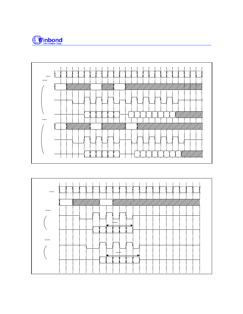
W942516CH
Publication Release Date: May 20, 2003
- 39 -
Revision A2
Timing Waveforms, continued
10.13 Read Interrupted by Write & BST (BL = 8)
READ
CMD
DQS
DQ
CLK
CLK
BST
Q0
Q1
Q2
Q3
Q4
Q5
CAS Latency=2
WRIT
D0
D1
D2
D3
D4
D5
D6
D7
READ
CMD
DQS
DQ
BST
Q0
Q1
Q2
Q3
Q4
Q5
CAS Latency=2.5
WRIT
D0
D1
D2
D3
D4
D5
D6
D7
Burst Read cycle must be terminated by BST Command to avoid I/O conflict.
10.14 Read Interrupted by Precharge (BL = 8)
READ
CMD
DQS
DQ
CLK
CLK
PRE
Q0
Q1
Q2
Q3
Q4
Q5
Q0
Q1
Q2
Q3
Q4
Q5
CAS Latency
CAS Latency
CAS Latency=2
DQS
DQ
CAS Latency=2.5
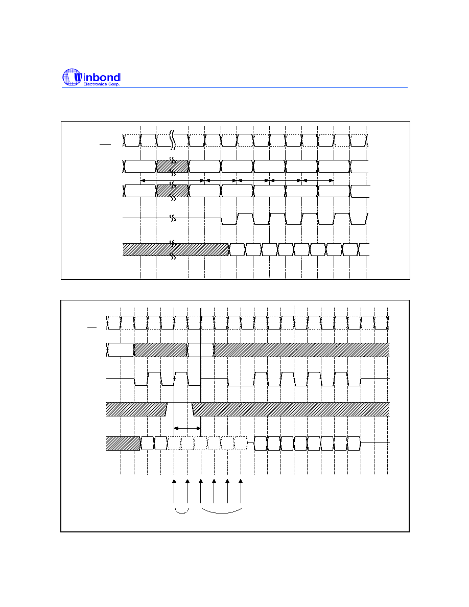
W942516CH
- 40 -
Timing Waveforms, continued
10.15 Write Interrupted by Write (BL = 2, 4, 8)
CMD
ADD
DQS
CLK
CLK
DQ
ACT
WRIT A
WRIT B
WRIT C
WRIT D
WRIT E
Row
Address
COl. Add. A
Col.Add.B
Col. Add. C
Col. Add. D
Col. Add. E
DC0
DC1
DD0
DD1
DA0
DA1
DB0
DB1
t
CCD
t
CCD
t
CCD
t
CCD
t
RCD
10.16 Write Interrupted by Read (CL = 2, BL = 8)
WRIT
CMD
DQS
DM
CLK
CLK
t
WTR
DQ
D4
D5
D6
D7
D0
D1
D2
D3
Data must be
masked by DM
READ
Data masked by READ
command, DQS input ignored.
Q4
Q5
Q6
Q7
Q0
Q1
Q2
Q3
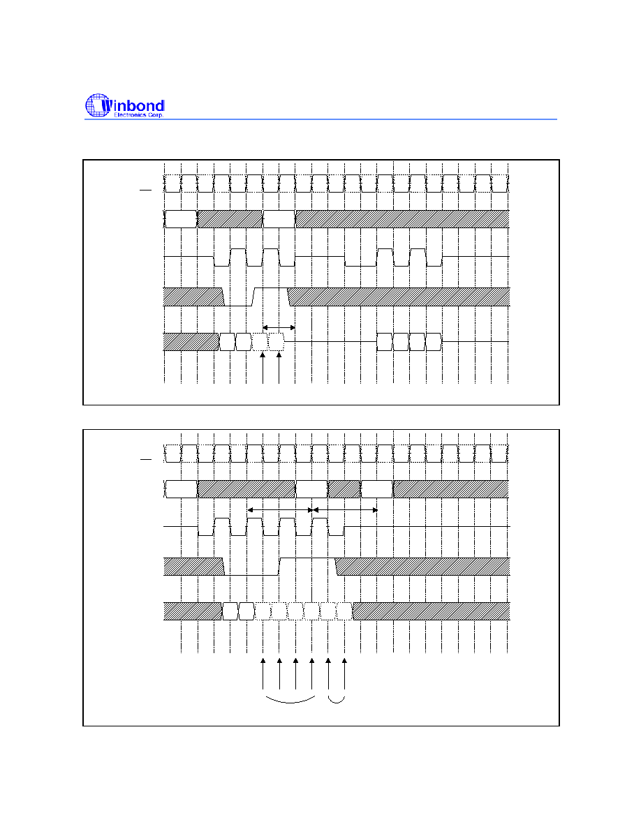
W942516CH
Publication Release Date: May 20, 2003
- 41 -
Revision A2
Timing Waveforms, continued
10.17 Write Interrupted by Read (CL = 2.5, BL = 4)
WRIT
CMD
DQS
DM
CLK
CLK
READ
t
WTR
DQ
Q0
Q1
Q2
Q3
D0
D1
D2
D3
Data must be masked by DM
10.18 Write Interrupted by Precharge (BL = 8)
WRIT
CMD
DQS
DM
CLK
CLK
ACT
t
WR
DQ
D4
D5
D6
D7
D0
D1
D2
D3
Data must be
masked by DM
PRE
t
RP
Data masked by PRE
command, DQS input ignored.
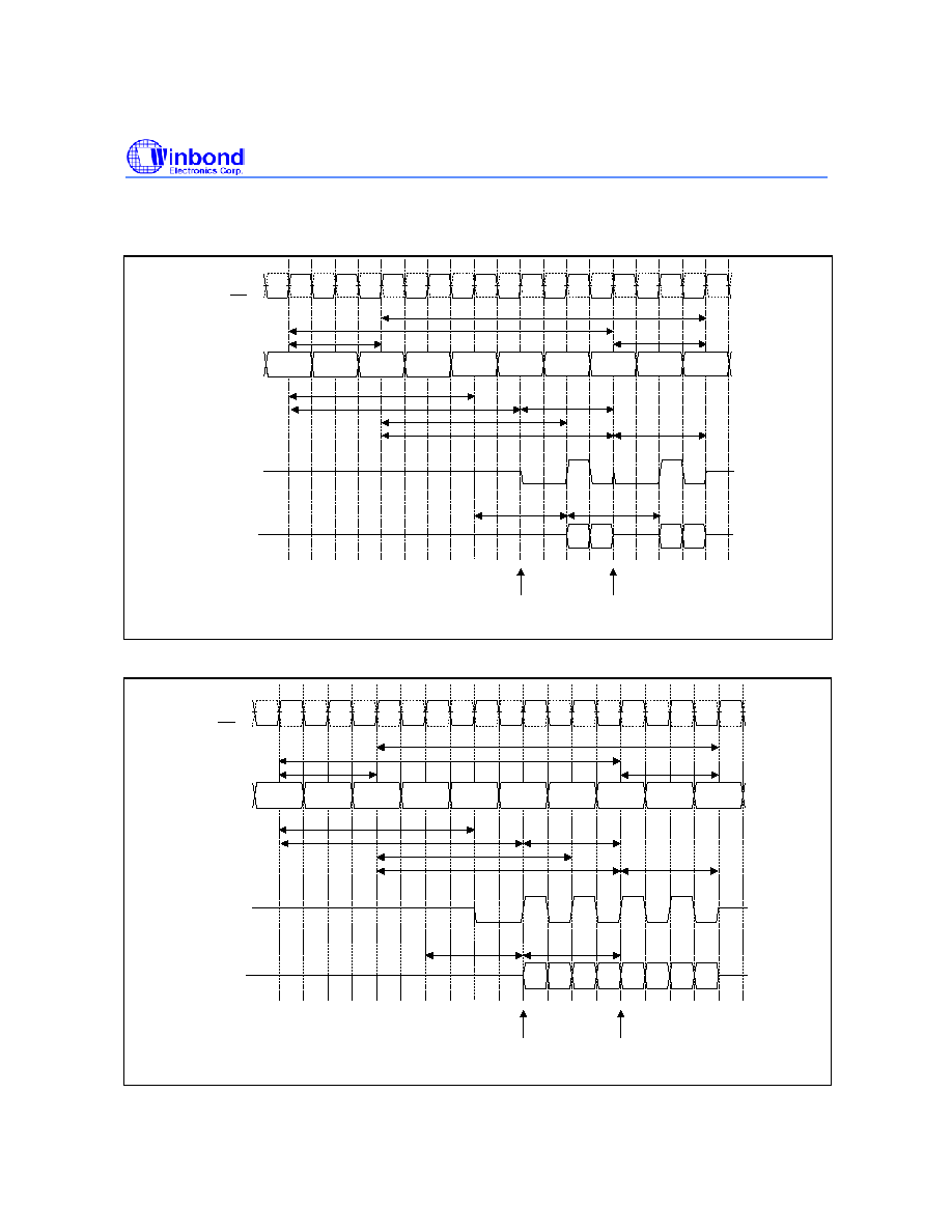
W942516CH
- 42 -
Timing Waveforms, continued
10.19 2 Bank Interleave Read Operation (CL = 2, BL = 2)
tCK = 100 MHz
CMD
DQS
CLK
CLK
DQ
Q0a
Q1a
Q0b
Q1b
ACTa/b : Bank Act. CMD of bank a/b
READAa/b : Read with Auto Pre.CMD of bank a/b
APa/b : Auto Pre. of bank a/b
ACTa
ACTb
READAa
ACTa
READAb
ACTb
APa
APb
t
RCD(a)
t
RAS(a)
t
RP(a)
t
RAS(b)
t
RCD(b)
t
RP(b)
CL(a)
CL(b)
Preamble Postamble Preamble
Postamble
t
RRD
t
RC(a)
t
RC(b)
t
RRD
10.20 2 Bank Interleave Read Operation (CL = 2, BL = 4)
CMD
DQS
CLK
CLK
DQ
Q2a
Q3a
Q2b
Q3b
ACTa/b : Bank Act. CMD of bank a/b
READAa/b : Read with Auto Pre.CMD of bank a/b
APa/b : Auto Pre. of bank a/b
ACTa
READAa
ACTb
READAb
ACTa
ACTb
APa
APb
t
RCD(a)
t
RAS(a)
t
RP(a)
t
RAS(b)
t
RCD(b)
t
RP(b)
CL(a)
CL(b)
Preamble
Postamble
t
RRD
t
RC(a)
t
RC(b)
t
RRD
Q0a
Q1a
Q0b
Q1b
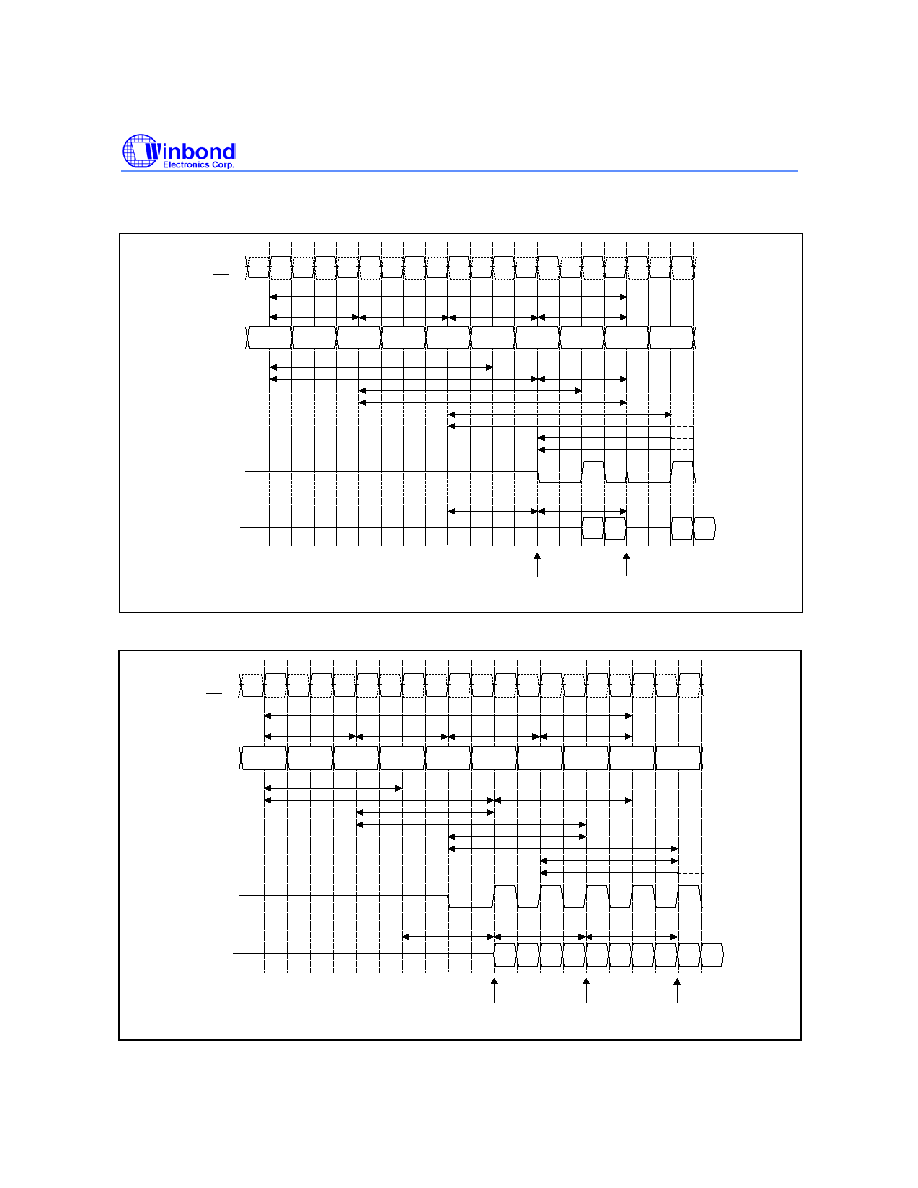
W942516CH
Publication Release Date: May 20, 2003
- 43 -
Revision A2
Timing Waveforms, continued
10.21 4 Bank Interleave Read Operation (CL = 2, BL = 2)
CMD
DQS
CLK
CLK
DQ
Q0a
Q1a
Q0b
Q1b
ACTa/b/c/d : Bank Act. CMD of bank a/b/c/d
READAa/b/c/d : Read with Auto Pre.CMD of bank a/b/c/d
APa/b/c/d : Auto Pre. of bank a/b/c/d
ACTa
ACTb
READAa
ACTc
READAb
ACTd
READAc
ACTa
APa
APb
t
RCD(a)
t
RAS(a)
t
RP
t
RAS(b)
t
RCD(b)
CL(a)
CL(b)
Preamble
Postamble Preamble
t
RRD
t
RC(a)
t
RRD
t
RAS(c)
t
RAS(d)
t
RCD(d)
t
RCD(c)
t
RRD
t
RRD
10.22 4 Bank Interleave Read Operation (CL = 2, BL = 4)
CMD
DQS
CLK
CLK
DQ
ACTa/b/c/d : Bank Act. CMD of bank a/b/c/d
READAa/b/c/d : Read with Auto Pre.CMD of bank a/b/c/d
APa/b/c/d : Auto Pre. of bank a/b/c/d
ACTa
READAa
ACTb
READAb
ACTc
READAc
ACTd
READAd
ACTa
APa
APb
t
RCD(a)
t
RAS(a)
t
RP(a)
t
RAS(b)
t
RCD(b)
CL(a)
CL(b)
t
RRD
t
RC(a)
t
RRD
t
RAS(c)
t
RAS(d)
t
RCD(d)
t
RCD(c)
t
RRD
t
RRD
Q2a
Q3a
Q2b
Q3b
CL(c)
Preamble
Q0a
Q1a
Q0b
Q1b
Q0a
Q1a
CL(b)
CL(b)
APc
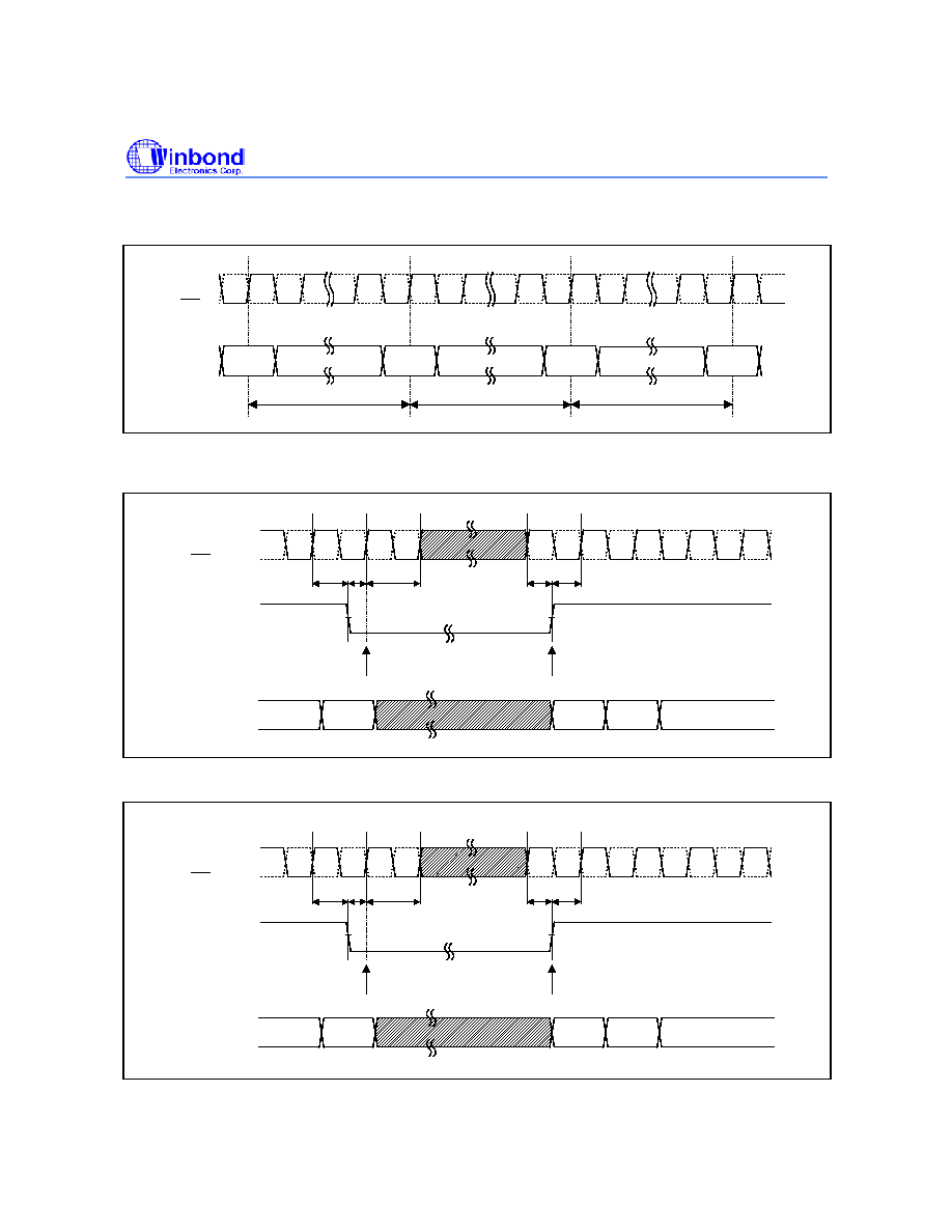
W942516CH
- 44 -
Timing Waveforms, continued
10.23 Auto Refresh Cycle
CMD
CLK
CLK
PREA
AREF
AREF
CMD
NOP
NOP
NOP
t
RP
t
RFC
t
RFC
CKE has to be kept "High" level for Auto-Refresh cycle.
10.24 Active Power Down Mode Entry and Exit Timing
CMD
CLK
CLK
NOP
CMD
NOP
Exit
Entry
NOP
NOP
t
IH
t
IS
t
CK
t
IH
t
IS
CKE
10.25 Precharged Power Down Mode Entry and Exit Timing
CMD
CLK
CLK
NOP
CMD
NOP
Exit
Entry
NOP
NOP
t
IH
t
IS
t
CK
t
IH
t
IS
CKE
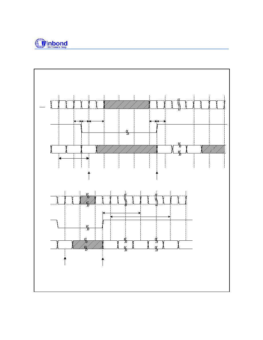
W942516CH
Publication Release Date: May 20, 2003
- 45 -
Revision A2
Timing Waveforms, continued
10.26 Self Refresh Entry and Exit Timing
CMD
CLK
CLK
t
IH
t
IS
t
CK
t
IH
t
IS
SELF
CMD
SELFX
NOP
NOP
PREA
Exit
Entry
CKE
t
RP
t
XSRD
NOP
SELF
t
XSNR
SELFX
NOP
ACT
READ
NOP
Exit
Entry
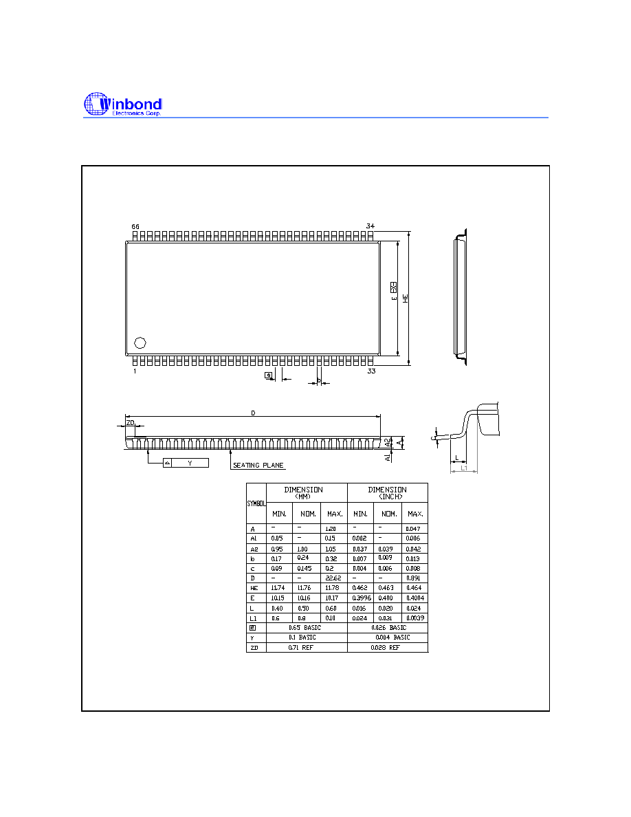
W942516CH
- 46 -
11. PACKAGE DIMENSION
TSOP 66l � 400 mil
W942516CH
Publication Release Date: May 20, 2003
- 47 -
Revision A2
12. REVISION HISTORY
REVISION DATE PAGE
DESCRIPTION
Aug. 28, 2002
- Preliminary
datasheet
Jan. 9, 2003
28
Add CAS Latency = 3 option
A1
Feb. 14, 2003
-
Modified AC timing spec.
A2
May 20, 2003
Add CL2.5 optional in DDR400
Headquarters
No. 4, Creation Rd. III,
Science-Based Industrial Park,
Hsinchu, Taiwan
TEL: 886-3-5770066
FAX: 886-3-5665577
http://www.winbond.com.tw/
Taipei Office
TEL: 886-2-8177-7168
FAX: 886-2-8751-3579
Winbond Electronics Corporation America
2727 North First Street, San Jose,
CA 95134, U.S.A.
TEL: 1-408-9436666
FAX: 1-408-5441798
Winbond Electronics (H.K.) Ltd.
No. 378 Kwun Tong Rd.,
Kowloon, Hong Kong
FAX: 852-27552064
Unit 9-15, 22F, Millennium City,
TEL: 852-27513100
Please note that all data and specifications are subject to change without notice.
All the trade marks of products and companies mentioned in this data sheet belong to their respective owners.
Winbond Electronics (Shanghai) Ltd.
200336 China
FAX: 86-21-62365998
27F, 2299 Yan An W. Rd. Shanghai,
TEL: 86-21-62365999
Winbond Electronics Corporation Japan
Shinyokohama Kohoku-ku,
Yokohama, 222-0033
FAX: 81-45-4781800
7F Daini-ueno BLDG, 3-7-18
TEL: 81-45-4781881
9F, No.480, Rueiguang Rd.,
Neihu District, Taipei, 114,
Taiwan, R.O.C.