 | –≠–ª–µ–∫—Ç—Ä–æ–Ω–Ω—ã–π –∫–æ–º–ø–æ–Ω–µ–Ω—Ç: KA3843A | –°–∫–∞—á–∞—Ç—å:  PDF PDF  ZIP ZIP |
Current Mode PWM Cont roller
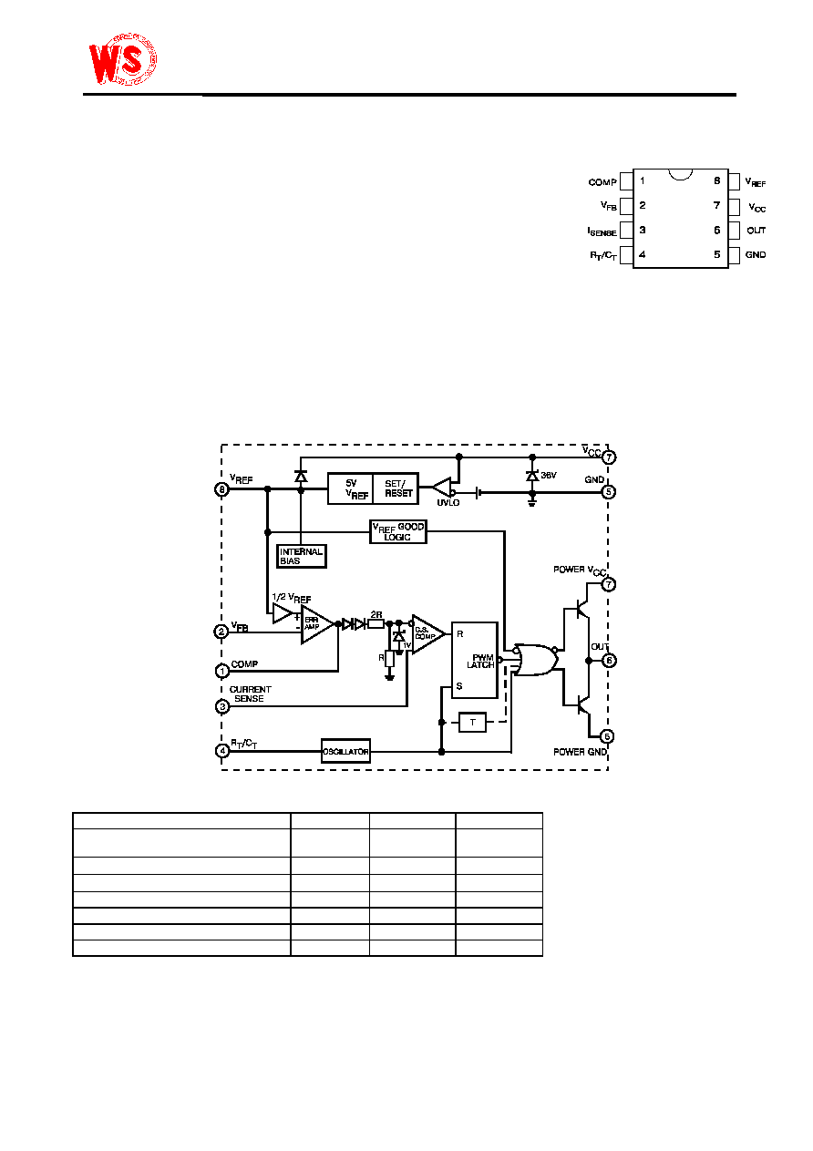
1
PIN
CONNECTION
(TOP VIEW)
DESCRIPTION
are fixed frequency current mode PWM
controller. They are specially designed for OFF
-Line and DC to DC converter applications
with a minimal external components. Internally implemented circuits include a trimmed
oscillator for precise duty cycle control, a temperature compensated reference, high gain
error amplifier, current sensing comparator, and a high current totempole output ideally
suited for driving a power MOSFET. Protection circuitry includes built undervoltage lockout
and current limiting.
The corresponding thresholds for the
can operate within 100% duty cycle.
has Start-Up Current 0.17mA (typ).
FEATURES
∑ Low Start-Up and Operating Current
∑ High Current Totem Pole Output
∑ Undervoltage Lockout With Hysteresis
∑ Operating Frequency Up To
BLOCK DIAGRAM
Absolute Maximum Ratings
Characteristic Symbol
Value
Unit
Supply Voltage (low impedance
source)
V
CC
30 V
Output Current
I
O
±1
A
Input Voltage (Analog Inputs pins 2,3)
V
I
-0.3 to 5.5
V
Error Amp Output Sink Current
I
SINK (E.A)
10
mA
Power Dissipation (T
A
=25
0
C) P
O
1 W
Storage Temperature Range
Tstg
-65 to150
o
C
Lead Temperature (soldering 5 sec.)
T
L
260
o
C
KA3843A(AM)
The KA3843AM
The KA3843AM are 8.4V(on) and 7.6V (off)
The KA3843AM
The KA3843AM
500KHz

Current Mode PWM Cont roller
2
Electrical characteristics (*V
CC
=15V, R
T
=10k
, C
T
=3.3nF, T
A
=0
0
C to +70
0
C, unless otherwise
specified)
Characteristics Symbol
Test
Condition
Min
Typ
Max
Unit
Reference Section
Reference Output Voltage
V
REF
T
J
= 25
∞C, I
REF
= 1 mA
4.9 5.0 5.1 V
Line Regulation
V
REF
12V
V
CC
25 V
6.0 20 mV
Load Regulation
V
REF
1 mA
I
REF
20mA
6.0
25
Short Circuit Output Current
I
SC
T
A
= 25
∞C
-100
-180
mA
Oscillator Section
384XA 47 50 57
Oscillation Frequency
f
T
J
= 25
∞C
384XAM
47 52 57
KHz
Frequency Change with
Voltage
f/V
CC
12V
V
CC
25 V
0.05
1.0
%
Oscillator Amplitude
V
(OSC)
(peak to peak)
1.6
V
Error Amplifier Section
Input Bias Current
I
BIAS
V
FB
=3V
-0.1
-2
µA
Input Voltage
V
I(E.A)
V
pin1
= 2.5V
2.42
2.5
2.58
V
Open Loop Voltage Gain
A
VOL
2V
V
0
4V
65 90
Power Supply Rejection Ratio
PSRR
12V
V
CC
25 V
60 70
dB
Output Sink Current
I
SINK
V
pin2
= 2.7V, V
pin1
= 1.1V
2
7
mA
Output Source Current
I
SOURCE
V
pin2
= 2.3V, V
pin1
= 5V
-0.5
-1.0
mA
High Output Voltage
V
OH
V
pin2
= 2.3V, R
L
= 15K
to GND
5.0 6.0
Low Output Voltage
V
OL
V
pin2
= 2.7V, R
L
= 15K
to PIN 8
0.8
1.1
V
Current Sense Section
Gain G
V
(Note 1 & 2)
2.85
3.0
3.15
V/V
Maximum Input Signal
V
I(MAX)
V
pin1
= 5V (Note1)
0.9
1.0
1.1
V
Supply Voltage Rejection
SVR
12V
V
CC
25 V (Note 1)
70 dB
Input Bias Current
I
BIAS
V
pin3
= 3V
-3.0
-10
µA
Output Section
Low Output Voltage
V
OL
I
SINK
= 20 mA
0.08
0.4
I
SINK
= 200 mA
1.4
2.2
High Output Voltage
V
OH
I
SINK
= 20 mA
13
13.5
I
SINK
= 200 mA
12
13.0
V
Rise Time
t
R
T
J
= 25
∞C, C
L
= 1nF (Note 3)
45
150
Fall Time
t
F
T
J
= 25
∞C, C
L
= 1nF (Note 3)
35
150
nS
Undervoltage Lockout Section
Start Theshold
V
TH(ST)
3843A(AM)
7.8
8.4
9.0
V
Min. Operating Voltage
V
OPR(min)
(After Turn On) 3843A(AM)/45A(AM) 7.0 7.6 8.2
V
PWM Section
Max. Duty Cycle D
(MAX)
3842A(AM)/43A(AM) 95 97 100
%
Min. Duty Cycle
D
(MAX)
0
Total Standby Current
Start
-Up Current I
ST
384XA(AM) 0.17 0.3
Operating Supply Current
I
CC (OPR)
V
pin3
= V
pin2
= 0V
13
17
mA
Zener Voltage
V
Z
I
CC
=25 mA
30
38
V
* Adjust V
CC
above the start threshold before setting it to 15V.
Note 1: Parameter measured at trip point of latch with V
pin2
=0.
Note 2: Gain defined as A=
V
pin1
/
V
pin3
; 0
V
pin3
0.8V.
Note 3: These parameters, although guaranteed, are not 100% tested in production.
KA3843A(AM)

Current Mode PWM Cont roller
3
PIN FUNCTION
N FUNCTION
DESCRIPTION
1 COMP
This pin is the Error Amplifier output and is made for loop compensation.
2 V
FB
This is the inverting input of the Error Amplifier. It is normally connected to the
switching power supply output through a resistor divider.
3 I
SENSE
A voltage proportional to inductor current is connected to this input. The PWM
uses this information to terminate the output switch conduction.
4 R
T
/C
T
The oscillator frequency and maximum Output duty cycle are programmed by
connecting resistor R
T
to V
ref
and capacitor C
T
to ground.
5 GROUND
This pin is the combined control circuitry and power ground.
6 OUTPUT
This output directly drives the gate of a power MOSFET. Peak currents up to 1A
are sourced and sink by this pin.
7 V
CC
This pin is the positive supply of the integrated circuit.
8 V
ref
This is the reference output. It provides charging current for capacitor C
T
through
resistor R
T
.
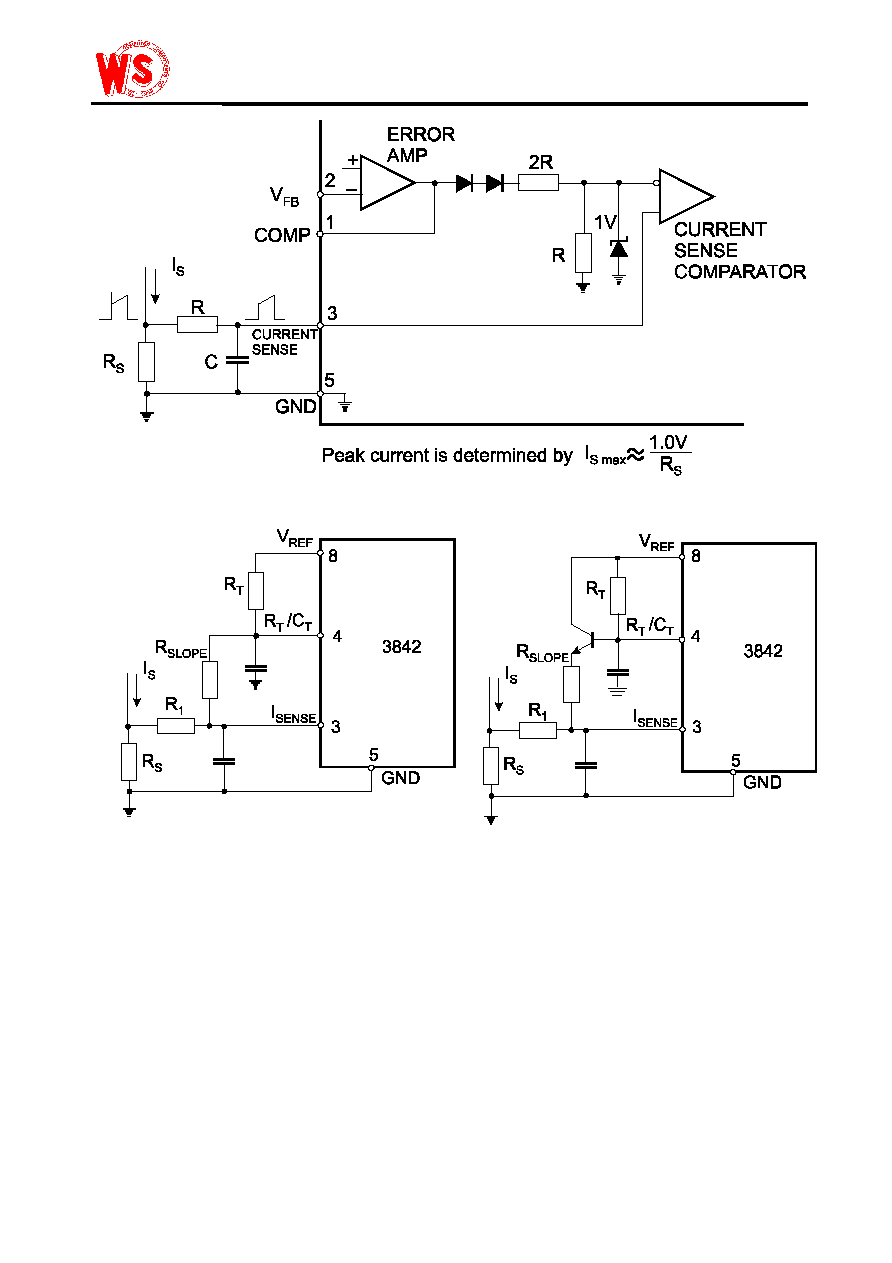
APPLICATION INFORMATION
Figure 1. Error Amp Configuration
Figure 2. Undervoltage Lockout
KA3843A(AM)
WS
WS
Current Mode PWM Cont roller
4
Figure 3. Current Sense Circuit
Figure 4. Slope Compensation Techniques
KA3843A(AM)

Current Mode PWM Cont roller
5
SCR must be selected for a holding current of less than 0.5mA.
The simple two transistor circuit can be used in place of the SCR as shown.
Figure 5. Latched Shutdown
Figure 6. Error Amplifier Compensation
KA3843A(AM)