 | –≠–ª–µ–∫—Ç—Ä–æ–Ω–Ω—ã–π –∫–æ–º–ø–æ–Ω–µ–Ω—Ç: WFP7N60 | –°–∫–∞—á–∞—Ç—å:  PDF PDF  ZIP ZIP |
Absolute Maximum Ratings
Symbol
Parameter
Value
Units
V
DSS
Drain to Source Voltage
600
V
I
D
Continuous Drain Current(@T
C
= 25
∞C)
7.0
A
Continuous Drain Current(@T
C
= 100
∞C)
4.4
A
I
DM
Drain Current Pulsed
(Note 1)
28
A
V
GS
Gate to Source Voltage
±
30
V
E
AS
Single Pulsed Avalanche Energy
(Note 2)
420
mJ
E
AR
Repetitive Avalanche Energy
(Note 1)
14.7
mJ
dv/dt
Peak Diode Recovery dv/dt
(Note 3)
4.5
V/ns
P
D
Total Power Dissipation(@T
C
= 25 ∞C)
147
W
Derating Factor above 25 ∞C
1.18
W/∞C
T
STG,
T
J
Operating Junction Temperature & Storage Temperature
- 55 ~ 150
∞C
T
L
Maximum Lead Temperature for soldering purpose,
1/8 from Case for 5 seconds.
300
∞C
Thermal Characteristics
Symbol
Parameter
Value
Units
Min.
Typ.
Max.
R
JC
Thermal Resistance, Junction-to-Case
-
-
0.85
∞C/W
R
CS
Thermal Resistance, Case to Sink
-
0.5
-
∞C/W
R
JA
Thermal Resistance, Junction-to-Ambient
-
-
62.5
∞C/W
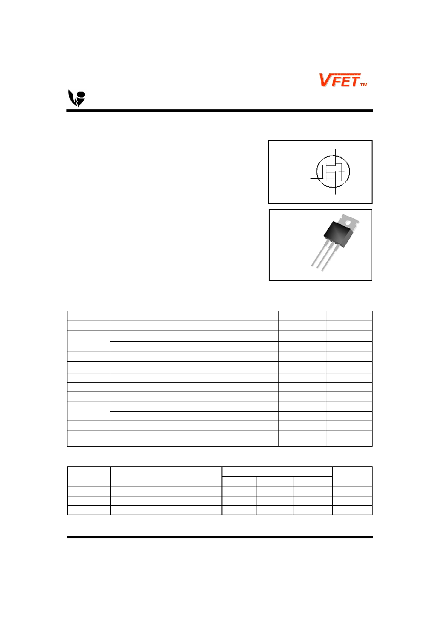
WFP7N60
Features
R
DS(on)
(Max 1.2 )@V
GS
=10V
Gate Charge (Typical 28nC)
Improved dv/dt Capability, High Ruggedness
100% Avalanche Tested
Maximum Junction Temperature Range (150∞C)
General Description
This Power MOSFET is produced using Wisdom's advanced
planar stripe, DMOS technology. This latest technology has been
especially designed to minimize on-state resistance, have a high
rugged avalanche characteristics. These devices are well suited
for high efficiency switch mode power supplies, active power factor
correction, electronic lamp ballasts based on half bridge topology.
N-Channel MOSFET
Wisdom
Semiconductor
Copyright@Wisdom Semiconductor Inc., All rights reserved.
Symbol
2. Drain
3. Source
1. Gate
TO-220
1 2
3
Electrical Characteristics
( T
C
= 25 ∞C unless otherwise noted )
Symbol
Parameter
Test Conditions
Min
Typ
Max
Units
Off Characteristics
BV
DSS
Drain-Source Breakdown Voltage
V
GS
= 0V, I
D
= 250uA
600
-
-
V
BV
DSS
/
T
J
Breakdown Voltage Temperature
coefficient
I
D
= 250uA, referenced to 25 ∞C
-
0.6
-
V/∞C
I
DSS
Drain-Source Leakage Current
V
DS
= 600V, V
GS
= 0V
-
-
10
uA
V
DS
= 480V, T
C
= 125 ∞C
-
-
100
uA
I
GSS
Gate-Source Leakage, Forward
V
GS
= 30V, V
DS
= 0V
-
-
100
nA
Gate-source Leakage, Reverse
V
GS
= -30V, V
DS
= 0V
-
-
-100
nA
On Characteristics
V
GS(th)
Gate Threshold Voltage
V
DS
= V
GS
, I
D
= 250uA
2.0
-
4.0
V
R
DS(ON)
Static Drain-Source On-state Resis-
tance
V
GS
=10 V, I
D
= 3.5A
-
1.0
1.2
Dynamic Characteristics
C
iss
Input Capacitance
V
GS
=0 V, V
DS
=25V, f = 1MHz
-
1100
1500
pF
C
oss
Output Capacitance
-
110
150
C
rss
Reverse Transfer Capacitance
-
12
16
Dynamic Characteristics
t
d(on)
Turn-on Delay Time
V
DD
=300V, I
D
=7.0A, R
G
=25
(Note 4, 5)
-
15
40
ns
t
r
Rise Time
-
30
70
t
d(off)
Turn-off Delay Time
-
110
230
t
f
Fall Time
-
40
90
Q
g
Total Gate Charge
V
DS
=480V, V
GS
=10V, I
D
=7.0A
(Note 4, 5)
-
28
37
nC
Q
gs
Gate-Source Charge
-
5
-
Q
gd
Gate-Drain Charge(Miller Charge)
-
11
-
Source-Drain Diode Ratings and Characteristics
Symbol
Parameter
Test Conditions
Min.
Typ.
Max.
Unit.
I
S
Continuous Source Current
Integral Reverse p-n Junction
Diode in the MOSFET
-
-
7.0
A
I
SM
Pulsed Source Current
-
-
28
V
SD
Diode Forward Voltage
I
S
=7.0A, V
GS
=0V
-
-
1.4
V
t
rr
Reverse Recovery Time
I
S
=7.0A, V
GS
=0V, dI
F
/dt=100A/us
-
365
-
ns
Q
rr
Reverse Recovery Charge
-
3.4
-
uC
WFP7N60
NOTES
1. Repeativity rating : pulse width limited by junction temperature
2. L = 15.7mH, I
AS
=7A, V
DD
= 50V, R
G
= 25 , Starting T
J
= 25∞C
3. I
SD
7A, di/dt 200A/us, V
DD
BV
DSS
, Starting T
J
= 25∞C
4. Pulse Test : Pulse Width 300us, Duty Cycle 2%
5. Essentially independent of operating temperature.
Copyright@Wisdom Semiconductor Inc., All rights reserved.

0
5
10
15
20
25
30
35
0
2
4
6
8
10
12
V
DS
= 300V
V
DS
= 120V
V
DS
= 480V
Note : I
D
= 7.0 A
V
GS
,
G
a
te
-So
u
rce Voltag
e [
V
]
Q
G
, Total Gate Charge [nC]
10
-1
10
0
10
1
0
500
1000
1500
2000
C
oss
C
iss
= C
gs
+ C
gd
(C
ds
= shorted)
C
oss
= C
ds
+ C
gd
C
rss
= C
gd
Notes :
1. V
GS
= 0 V
2. f = 1 MHz
C
rss
C
iss
Ca
pa
cit
a
nce
[p
F]
V
DS
, Drain-Source Voltage [V]
0.2
0.4
0.6
0.8
1.0
1.2
1.4
10
-1
10
0
10
1
150
Notes :
1. V
GS
= 0V
2. 250µs Pulse Test
25
I
DR
,
Rever
s
e
D
r
ai
n Cur
r
ent
[
A
]
V
SD
, Source-Drain voltage [V]
0
5
10
15
20
25
0
1
2
3
4
5
V
GS
= 20V
V
GS
= 10V
Note : T
J
= 25
R
DS
(
O
N
)
[
],
D
r
ai
n
-
S
ourc
e
O
n
-R
es
i
s
t
anc
e
I
D
, Drain Current [A]
2
4
6
8
10
10
-1
10
0
10
1
150
o
C
25
o
C
-55
o
C
Notes :
1. V
DS
= 40V
2. 250µs Pulse Test
I
D
,
Dr
ai
n Cu
r
r
ent
[
A
]
V
GS
, Gate-Source Voltage [V]
10
-1
10
0
10
1
10
-1
10
0
10
1
V
GS
Top : 15.0 V
10.0 V
8.0 V
7.0 V
6.5 V
6.0 V
5.5 V
Bottom : 5.0 V
Notes :
1. 250µs Pulse Test
2. T
C
= 25
I
D
,
Dr
a
i
n Cur
r
ent
[
A
]
V
DS
, Drain-Source Voltage [V]
Typical Characteristics
Figure 5. Capacitance Characteristics
Figure 6. Gate Charge Characteristics
Figure 3. On-Resistance Variation vs
Drain Current and Gate Voltage
Figure 4. Body Diode Forward Voltage
Variation with Source Current
and Temperature
Figure 2. Transfer Characteristics
Figure 1. On-Region Characteristics

1 0
-5
1 0
-4
1 0
-3
1 0
-2
1 0
-1
1 0
0
1 0
1
1 0
-2
1 0
-1
1 0
0
N o te s :
1 . Z
J C
(t) = 0 .8 5
/W M a x .
2 . D u ty F a c to r, D = t
1
/t
2
3 . T
J M
- T
C
= P
D M
* Z
J C
(t)
s in g le p u ls e
D = 0 .5
0 .0 2
0 .2
0 .0 5
0 .1
0 .0 1
Z
JC
(
t
)
,
T
her
m
a
l
R
e
spon
se
t
1
, S q u a re W a v e P u ls e D u ra tio n [s e c ]
25
50
75
100
125
150
0
2
4
6
8
I
D
, D
r
ain C
u
r
r
e
nt [A
]
T
C
, Case Temperature [ ]
10
0
10
1
10
2
10
3
10
-2
10
-1
10
0
10
1
10
2
10
µ
s
DC
10 ms
1 ms
100
µ
s
Operation in This Area
is Limited by R
DS(on)
Notes :
1. T
C
= 25
o
C
2. T
J
= 150
o
C
3. Single Pulse
I
D
,
Drai
n C
u
rrent
[
A
]
V
DS
, Drain-Source Voltage [V]
-100
-50
0
50
100
150
200
0.0
0.5
1.0
1.5
2.0
2.5
3.0
Notes :
1. V
GS
= 10 V
2. I
D
= 3.5 A
R
DS(
O
N)
,
(
N
or
m
a
l
i
z
ed
)
Dr
ai
n-
Sou
r
ce
O
n
-
R
es
i
s
t
a
n
c
e
T
J
, Junction Temperature [
o
C]
-100
-50
0
50
100
150
200
0.8
0.9
1.0
1.1
1.2
Notes :
1. V
GS
= 0 V
2. I
D
= 250 µA
BV
DS
S
, (Norm
a
l
i
zed)
Drai
n
-
So
urce B
r
ea
k
d
own
V
o
l
t
age
T
J
, Junction Temperature [
o
C]
Typical Characteristics
(Continued)
Figure 9. Maximum Safe Operating Area
Figure 10. Maximum Drain Current
vs Case Temperature
Figure 7. Breakdown Voltage Variation
vs Temperature
Figure 8. On-Resistance Variation
vs Temperature
Figure 11. Transient Thermal Response Curve
t
1
P
DM
t
2

C
harge
V
G
S
10V
Q
g
Q
gs
Q
gd
3m
A
V
G
S
D
U
T
V
D
S
300nF
50K
200nF
12V
S
am
e Type
as D
U
T
C
harge
V
G
S
10V
Q
g
Q
gs
Q
gd
3m
A
V
G
S
D
U
T
V
D
S
300nF
50K
200nF
12V
S
am
e Type
as D
U
T
V
G
S
V
D
S
1
0
%
9
0
%
t
d
(
o
n
)
t
r
t
o
n
t
o
ff
t
d
(
o
ff)
t
f
V
D
D
1
0
V
V
D
S
R
L
D
U
T
R
G
V
G
S
V
G
S
V
D
S
1
0
%
9
0
%
t
d
(
o
n
)
t
r
t
o
n
t
o
ff
t
d
(
o
ff)
t
f
V
D
D
1
0
V
V
D
S
R
L
D
U
T
R
G
V
G
S
E
A
S
=
L
I
A
S
2
----
2
1
--------------------
B
V
D
S
S
-V
D
D
B
V
D
S
S
V
D
D
V
D
S
B
V
D
S
S
t
p
V
D
D
I
A
S
V
D
S
(t)
I
D
(t)
T
im
e
1
0
V
D
U
T
R
G
L
I
D
t
p
E
A
S
=
L
I
A
S
2
----
2
1
E
A
S
=
L
I
A
S
2
----
2
1
----
2
1
--------------------
B
V
D
S
S
-V
D
D
B
V
D
S
S
V
D
D
V
D
S
B
V
D
S
S
t
p
V
D
D
I
A
S
V
D
S
(t)
I
D
(t)
T
im
e
1
0
V
D
U
T
R
G
L
L
I
D
I
D
t
p
Gate Charge Test Circuit & Waveform
Resistive Switching Test Circuit & Waveforms
Unclamped Inductive Switching Test Circuit & Waveforms