 | –≠–ª–µ–∫—Ç—Ä–æ–Ω–Ω—ã–π –∫–æ–º–ø–æ–Ω–µ–Ω—Ç: CV211-1 | –°–∫–∞—á–∞—Ç—å:  PDF PDF  ZIP ZIP |
Specifications and information are subject to change without notice
WJ Communications, Inc
∑
Phone 1-800-WJ1-4401
∑
FAX: 408-577-6621
∑
e-mail: sales@wj.com
∑
Web site: www.wj.com
October 2003
CV211-1
PCS/DCS-band Dual-Branch Downconverter
Product Information
The Communications Edge
TM
Product Features
∑
High dynamic range downconverter
with integrated LO and IF amplifiers
∑
Dual channels for diversity
∑
+29.5 dBm Input IP3
∑
+10 dBm Input P1dB
∑
RF: 1710 ≠ 2000 MHz
∑
IF: 65 ≠ 250 MHz
∑
Single supply operation (+5 V)
∑
6x6 mm 28-pin QFN package
∑
Low-side LO configuration
∑
Common footprint with other
PCS/UMTS/cellular versions
Product Description
The CV211-1 is a dual-channel high-linearity
downconverter designed to meet the demanding
performance, functionality, and cost goals of current and
next generation mobile infrastructure basestations. It
provides high dynamic range performance in a low profile
surface-mount leadless package that measures 6 x 6 mm
square.
It is ideally suited for high dynamic range receiver front
ends using diversity receive channels. Functionality
includes frequency conversion & IF amplification, while
an integrated LO driver amplifier powers the passive
mixer. The MCM is implemented with reliable and
mature GaAs MESFET and InGaP HBT technology.
Typical applications include frequency downconversion
used in PCS/DCS-band 2.5G and 3G mobile base
transceiver stations.
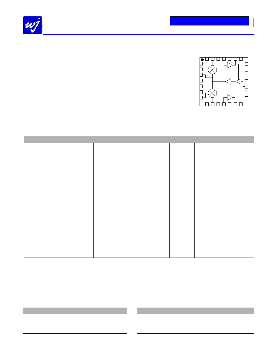
Functional Diagram
Top View
Specifications
1
Parameters
Units
Min
Typ
Max
Comments
RF Frequency Range
MHz
1710
2000
LO Frequency Range
MHz
1460
1935
IF Center Frequency Range
MHz
65
240
250
See note 2
% Bandwidth around IF center frequency
%
±7.5
See note 3
SSB Conversion Gain
dB
8
10
12
Temp = 25∞ C
Gain Drift over Temp (-40∞ C to 85∞ C)
dB
-1.5
±0.5
1.5
Referenced to +25∞ C
Input IP3
dBm
+25
+29.5
See note 4
Input IP2
dBm
+33
+38
See note 4
Input 1 dB Compression Point
dBm
+10
See note 4
Noise Figure
dB
11
See note 5
LO Input Drive Level
dBm
-2.5
0
+2.5
LO-RF Isolation
dB
8
P
LO
= 0 dBm
LO-IF Isolation
dB
32
P
LO
= 0 dBm
Branch-Branch Isolation
dB
45
Return Loss: RF Port
dB
18
Return Loss: LO Port
dB
15
Return Loss: IF Port
dB
12
Operating Supply Voltage
V
+5
Supply
Current
mA 320 380 475
Thermal Resistance
∞C / W
27
Junction Temperature
∞
C 160
See
note
6
1. Specifications when using the application specific circuit (shown on page 3) with a low side LO = 0 dBm in a downconverting application at 25
∞
C.
2. IF matching components affect the center IF frequency. Proper component values for other IF center frequencies than shown can be provided by emailing to applications.engineering@wj.com.
3. The IF bandwidth of the converter is defined as 15% around any center frequency in its operating IF frequency range. The bandwidth is determined with external components. Specifications are valid around
the total ±7.5% bandwidth. ie. with a center frequency of 240 MHz, the specifications are valid from 240 ± 18 MHz.
4. Assumes the supply voltage = +5 V. IIP3 is measured with
f = 1 MHz with RF
in
= -5 dBm / tone.
5. Assumes LO injection noise is filtered at the thermal noise floor, -174 dBm/Hz, at the RF, IF, and Image frequencies.
6. The maximum junction temperature ensures a minimum MTBF rating of 1 million hours of usage.
Absolute Maximum Rating
Ordering Information
Parameters
Rating
Part No.
Description
Operating Case Temperature
-40∞ to +85
∞
C
CV211-1
PCS/DCS-band Dual-Branch Downconverter
Storage Temperature
-55∞ to +125∞ C
CV211-1PCB240 Fully-Assembled Application Board, IF = 240 MHz
DC Voltage
+5.5 V
Junction Temperature
+220 ∞C
Operation of this device above any of these parameters may cause permanent damage.
1
2
3
4
5
6
7
21
20
19
18
17
16
15
28
27
26
25
24
23
22
8
9
10
11
12
13
14
IF Amp 2
IF Amp 1
LO Driver Amp
BIAS
GND
N/C
GND
LO
GND
N/C
RF 1
INPUT
GND
BIAS
GND
N/C
GND
GND
MIX
E
R
IF
1
GND
A
MP
1
IN
P
U
T
GND
GND
GND
MIX
E
R
IF
2
GND
GND
GND
IF
AM
P2
IN
P
U
T
IF
1
OUT
P
U
T
IF
2
OUT
P
U
T
IF
RF
RF
RF 2
INPUT
Specifications and information are subject to change without notice
WJ Communications, Inc
∑
Phone 1-800-WJ1-4401
∑
FAX: 408-577-6621
∑
e-mail: sales@wj.com
∑
Web site: www.wj.com
October 2003
CV211-1
PCS/DCS-band Dual-Branch Downconverter
Product Information
The Communications Edge
TM
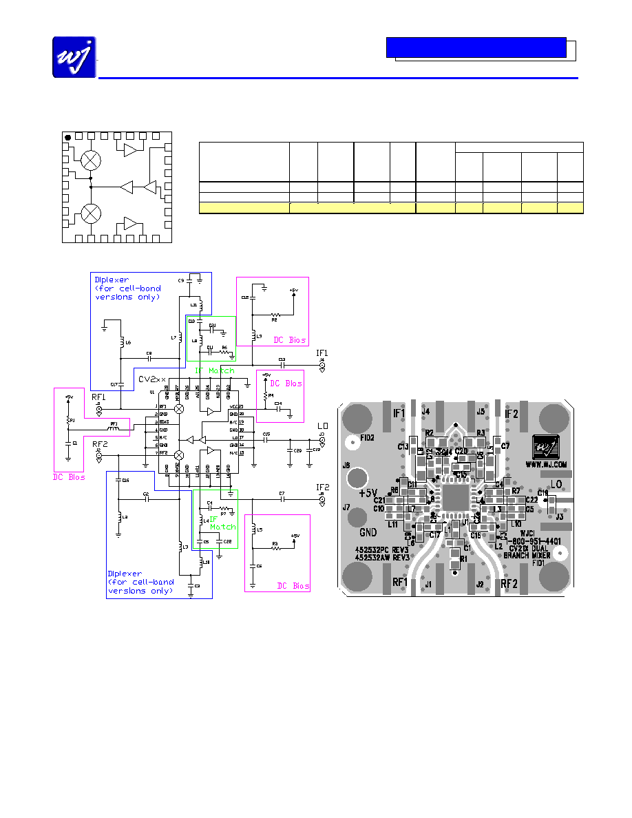
Device Architecture / Application Circuit Information
Typical Downconverter Performance Chain Analysis (Each Branch)
Cumulative Performance
Stage
Gain
(dB)
Input
P1dB
(dBm)
Input
IP3
(dBm)
NF
(dB)
Current
(mA)
Gain
(dB)
Input
P1dB
(dBm)
Input
IP3
(dBm)
NF
(dB)
LO Amp / MMIC Mixer
-9
11
30
9.3
80
-9
11
30
9.3
IF Amplifier
19
2
22
1.8
150
10
8
27.5
11
CV211-1
Cumulative Performance
380*
10
+8
+27.5
11
* The
2
nd
branch includes another mixer and IF amplifier, which increases the total current consumption
of the MCM to be 380 mA.
CV211-1: The application circuit can be broken up into three main
functions as denoted in the colored dotted areas above: RF/IF diplexing
(blue), IF amplifier matching (green), and dc biasing (purple). There are
various placeholders for chip components in the circuit schematic so that
a common PCB can be used for all WJ dual-branch converters. Further
details are given in the Application Note located on the website titled
"CV2xx Series - PWB Design Guidelines".
External Diplexer:
This is only used with the cellular-band CV
products. The mixer performs the diplexing internally for the
CV211-1; therefore the components shown in the diplexer section
should be not be loaded except for L3, L10, L7, and L11, which
should contain a 0
jumper.
IF Amplifier Matching:
The IF amplifier requires matching
elements to optimize the performance of the amplifier to the desired
IF center frequency. Since IF bandwidths are typically on the order
of 5 to 10%, a simple two element matching network, in the form of
either a high-pass or low-pass filter structure, is sufficient to match
the MMIC IF amplifier over these narrow bandwidths. Proper
component values for other IF center frequencies can be provided by
emailing to applications.engineering@wj.com.
DC biasing:
DC bias must be provided for the LO and IF amplifiers
in the converter. R1 sets the operating current for the last stage of the
LO amplifier and is chosen to optimize the mixer LO drive level.
Proper RF chokes and bypass capacitors are chosen for proper
amplifier biasing at the intended frequency of operation. The "+5 V"
dc bias should be supplied directly from a voltage regulator.
Printed Circuit Board Material:
.014" FR-4, 4 layers, .062" total thickness
1
2
3
4
5
6
7
21
20
19
18
17
16
15
28
27
26
25
24
23
22
8
9
10
11
12
13
14
IF Amp 2
IF Amp 1
LO Driver Amp
BIAS
GND
N/C
GND
LO
GND
N/C
RF 1
INPUT
GND
BIAS
GND
N/C
GND
GND
MIX
E
R
IF
1
GND
A
MP
1
IN
P
U
T
GND
GND
GND
MIX
E
R
IF
2
GND
GND
GND
IF
AM
P2
IN
P
U
T
IF
1
OUT
P
U
T
IF
2
OUT
P
U
T
IF
RF
RF
RF 2
INPUT
Specifications and information are subject to change without notice
WJ Communications, Inc
∑
Phone 1-800-WJ1-4401
∑
FAX: 408-577-6621
∑
e-mail: sales@wj.com
∑
Web site: www.wj.com
October 2003
CV211-1
PCS/DCS-band Dual-Branch Downconverter
Product Information
The Communications Edge
TM
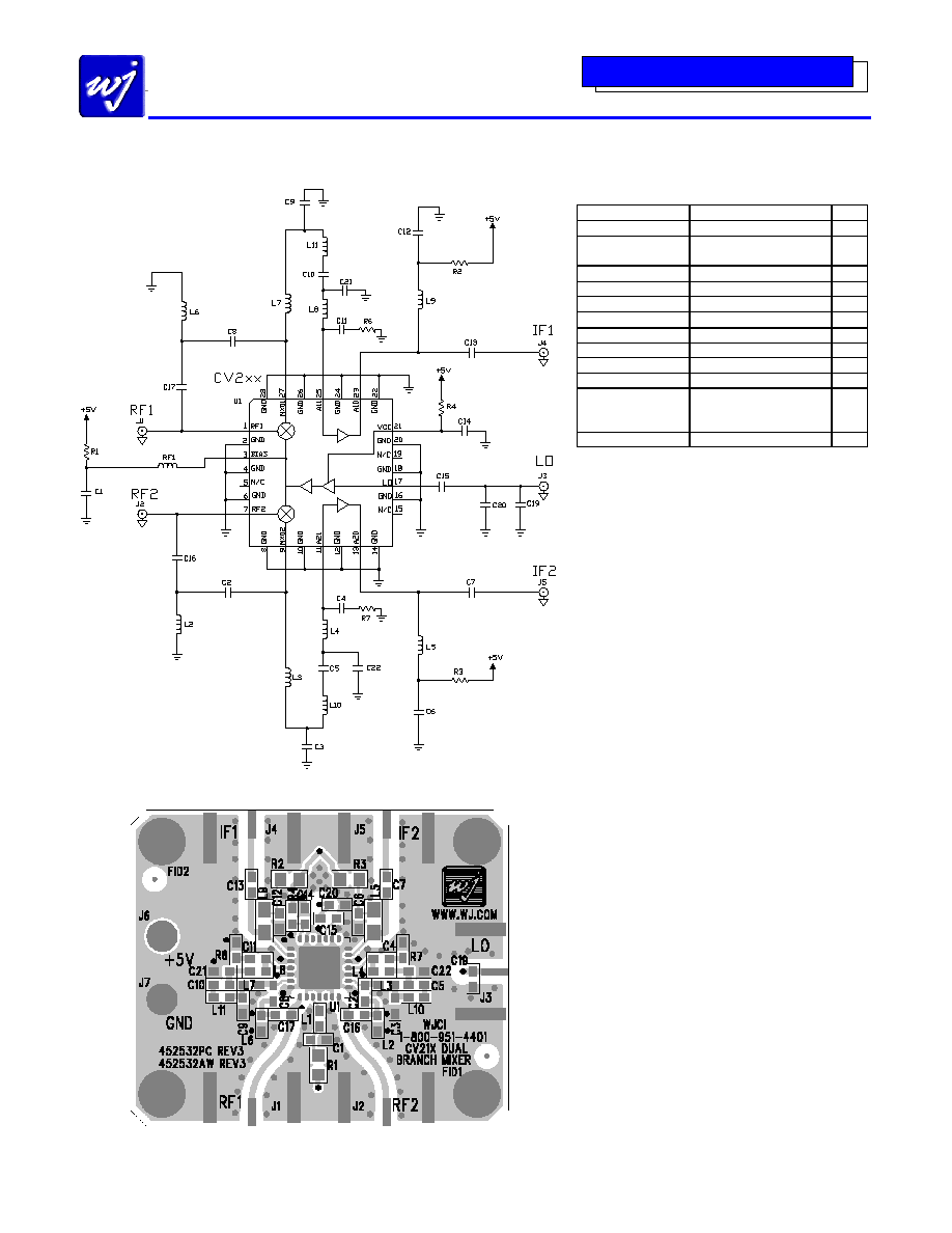
Application Circuit: IF = 240 MHz (CV211-1PCB240)
PCB Layout
Circuit Board Material: .014" FR-4, 4 layers, .062" total thickness
Bill of Materials
Ref. Desig.
Component
Size
R1
13
chip resistor
0805
R2, R3, R4, L3, L7
L10, L11
0
chip resistor
0603
R6, R7
2.2
chip resistor
0603
C1, C5, C10, C15
1000 pF chip capacitor
0603
C4, C11
2 pF chip capacitor
0603
C6, C12, C14
.01
µ
F chip capacitor
0603
C7, C13
100 pF chip capacitor
0603
L1
120 nH chip inductor
0603
L4, L8
56 nH chip inductor
0603
L5, L9
220 nH chip inductor
0805
C2, C3, C8, C9, C16
C17, C19, C20, C21
C22, L2, L6
Do Not Place
U1
CV211-1 WJ Converter
QFN
Specifications and information are subject to change without notice
WJ Communications, Inc
∑
Phone 1-800-WJ1-4401
∑
FAX: 408-577-6621
∑
e-mail: sales@wj.com
∑
Web site: www.wj.com
October 2003
CV211-1
PCS/DCS-band Dual-Branch Downconverter
Product Information
The Communications Edge
TM
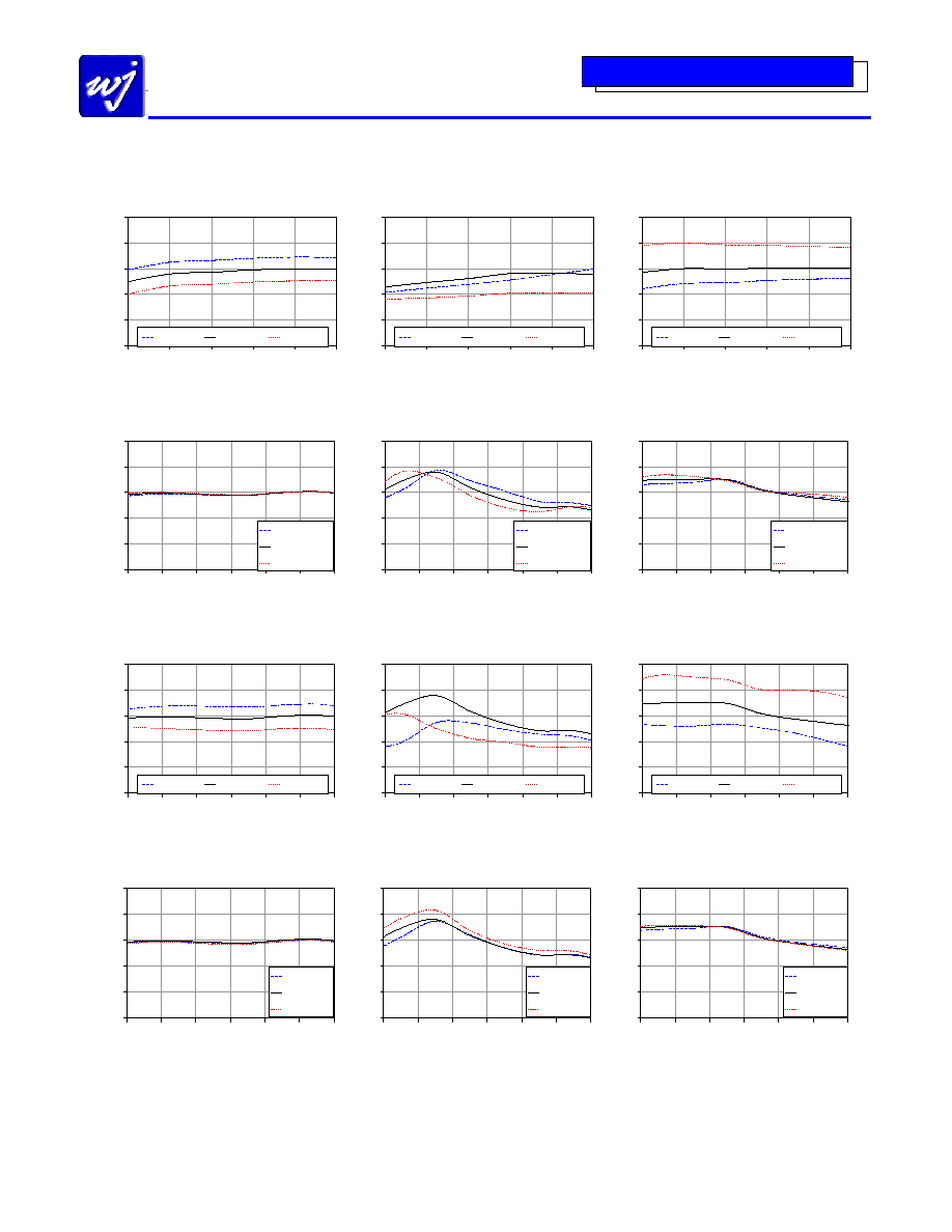
CV211-1PCB240 Application Circuit Performance Plots
Conversion Gain vs IF Frequency
LO = 0 dBm, 1640 MHz
7
8
9
10
11
12
215
225
235
245
255
265
IF Frequency (MHz)
Conversion Gain (dB)
-40 deg C
+25 deg C
+85 deg C
Input IP3 vs IF Frequency
LO = 0 dBm, 1640 MHz
24
26
28
30
32
34
215
225
235
245
255
265
IF Frequency (MHz)
Input IP3 (dBm)
-40 deg C
+25 deg C
+85 deg C
Input IP2 vs IF Frequency
LO = 0 dBm, 1640 MHz
32
34
36
38
40
42
215
225
235
245
255
265
IF Frequency (MHz)
Input IP2 (dBm)
-40 deg C
+25 deg C
+85 deg C
Conversion Gain vs RF Frequency
25 deg C, IF = 240 MHz
7
8
9
10
11
12
1700 1750 1800 1850 1900 1950 2000
RF Frequency (MHz)
Conversion Gain (dB)
LO = -2.5 dBm
LO = 0 dBm
LO = 2.5 dBm
Input IP3 vs RF Frequency
25 deg C, IF = 240 MHz
24
26
28
30
32
34
1700 1750 1800 1850 1900 1950 2000
RF Frequency (MHz)
Input IP3 (dBm)
LO = -2.5 dBm
LO = 0 dBm
LO = 2.5 dBm
Input IP2 vs RF Frequency
25 deg C, IF = 240 MHz, low-side LO
32
34
36
38
40
42
1700 1750 1800 1850 1900 1950 2000
RF Frequency (MHz)
Input IP2 (dBm)
LO = -2.5 dBm
LO = 0 dBm
LO = 2.5 dBm
Conversion Gain vs RF Frequency
LO = 0 dBm, IF = 240 MHz, low-side LO
7
8
9
10
11
12
1700 1750 1800 1850 1900 1950 2000
RF Frequency (MHz)
Conversion Gain (dB)
-40 deg C
+25 deg C
+85 deg C
Input IP3 vs RF Frequency
LO = 0 dBm, IF = 240 MHz, low-side LO
24
26
28
30
32
34
1700 1750 1800 1850 1900 1950 2000
RF Frequency (MHz)
Input IP3 (dBm)
-40 deg C
+25 deg C
+85 deg C
Input IP2 vs RF Frequency
LO = 0 dBm, IF = 240 MHz, low-side LO
32
34
36
38
40
42
1700 1750 1800 1850 1900 1950 2000
RF Frequency (MHz)
Input IP2 (dBm)
-40 deg C
+25 deg C
+85 deg C
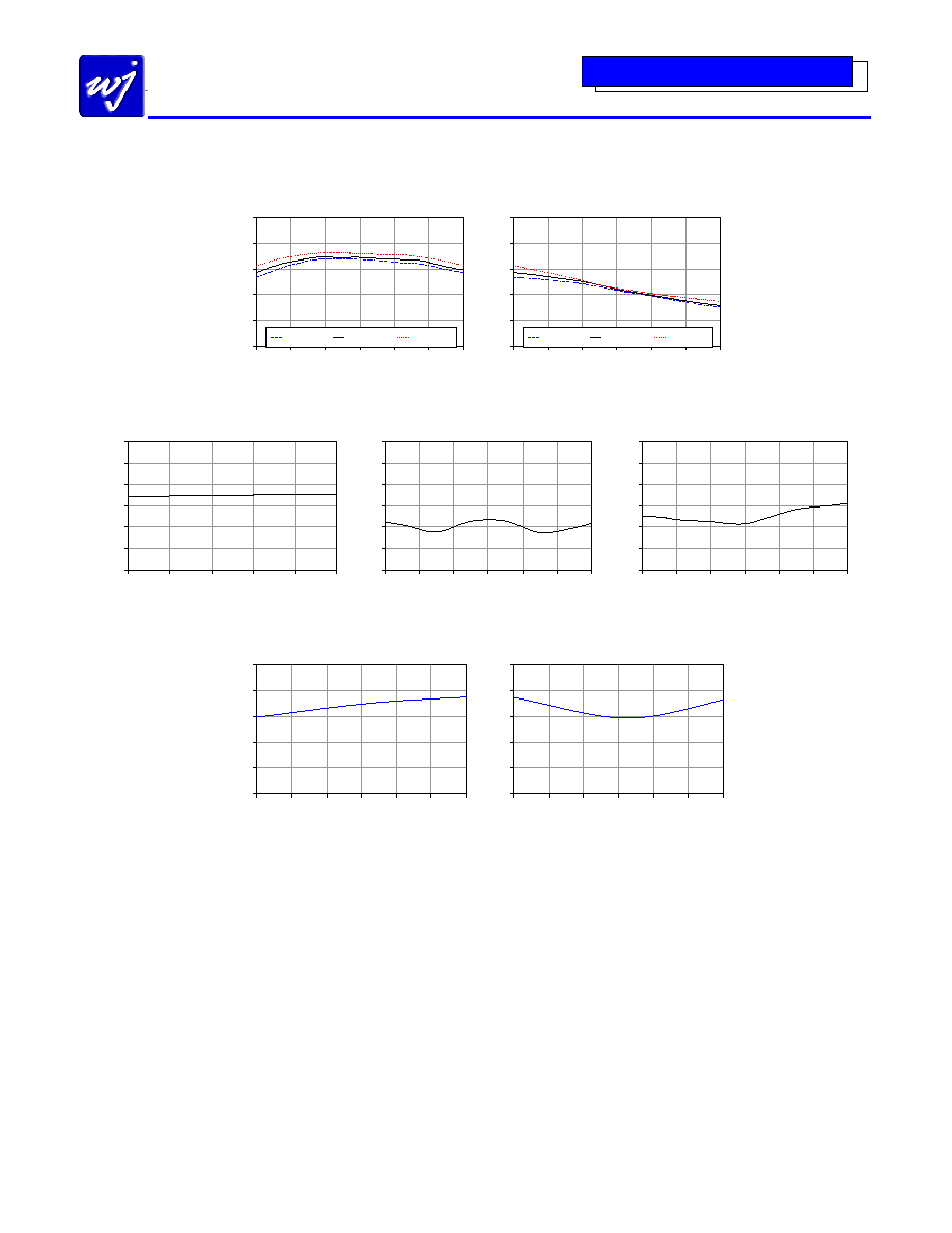
Conversion Gain vs RF Frequency
25 deg C, LO = 0 dBm, IF = 240 MHz, low-side LO
7
8
9
10
11
12
1700
1750
1800
1850
1900
1950
2000
RF Frequency (MHz)
Conversion Gain (dB)
Vdd = 4.9 V
Vdd = 5.0 V
Vdd = 5.1 V
Input IP3 vs RF Frequency
25 deg C, LO = 0 dBm, IF = 240 MHz, low-side LO
24
26
28
30
32
34
1700
1750
1800
1850
1900
1950
2000
RF Frequency (MHz)
Input IP3 (dBm)
Vdd = 4.9 V
Vdd = 5.0 V
Vdd = 5.1 V
Input IP2 vs RF Frequency
25 deg C, LO = 0 dBm, IF = 240 MHz, low-side LO
32
34
36
38
40
42
1700
1750
1800
1850
1900
1950
2000
RF Frequency (MHz)
Input IP2 (dBm)
Vdd = 4.9 V
Vdd = 5.0 V
Vdd = 5.1 V
Specifications and information are subject to change without notice
WJ Communications, Inc
∑
Phone 1-800-WJ1-4401
∑
FAX: 408-577-6621
∑
e-mail: sales@wj.com
∑
Web site: www.wj.com
October 2003
CV211-1
PCS/DCS-band Dual-Branch Downconverter
Product Information
The Communications Edge
TM
CV211-1PCB240 Application Circuit Performance Plots (cont'd)
L-I Isolation vs LO Frequency
Referenced with LO = 0 dBm
15
20
25
30
35
40
1400 1500 1600 1700 1800 1900 2000
LO Frequency (MHz)
L-I Isolation (dB)
-40 deg C
+25 deg C
+85 deg C
L-R Isolation vs LO Frequency
Referenced with LO = 0 dBm
0
5
10
15
20
25
1400 1500 1600 1700 1800 1900 2000
LO Frequency (MHz)
L-R Isolation (dB)
-40 deg C
+25 deg C
+85 deg C
IF Return Loss vs IF Frequency
25∞ C
0
5
10
15
20
25
30
215
225
235
245
255
265
IF Frequency (MHz)
Return Loss (dB)
RF Return Loss vs RF Frequency
25∞ C
0
5
10
15
20
25
30
1700 1750 1800 1850 1900 1950 2000
RF Frequency (MHz)
Return Loss (dB)
LO Return Loss vs LO Frequency
25∞ C
0
5
10
15
20
25
30
1400 1500 1600 1700 1800 1900 2000
LO Frequency (MHz)
Return Loss (dB)
Noise Figure vs Temperature
RF = 1880 MHz, IF = 240 MHz, LO = 0 dBm @ 1640 MHz
4
6
8
10
12
14
-40
-20
0
20
40
60
80
Temperature (∞C)
Noise Figure (dB)
Input P1dB vs Temperature
RF = 1880 MHz, IF = 240 MHz, LO = 0 dBm @ 1640 MHz
4
6
8
10
12
14
-40
-20
0
20
40
60
80
Temperature (∞C)
Input P1dB (dBm)