 | –≠–ª–µ–∫—Ç—Ä–æ–Ω–Ω—ã–π –∫–æ–º–ø–æ–Ω–µ–Ω—Ç: ECG014 | –°–∫–∞—á–∞—Ç—å:  PDF PDF  ZIP ZIP |
.
Specifications and information are subject to change without notice
WJ Communications, Inc
∑
Phone 1-800-WJ1-4401
∑
FAX: 408-577-6621
∑
e-mail: sales@wj.com
∑
Web site: www.wj.com
August
2004
ECG014
0.2 Watt, High Linearity InGaP HBT Amplifier
Product Information
The Communications Edge
TM
Product Features
∑
50 ≠ 2000 MHz
∑
+23 dBm P1dB
∑
+39 dBm Output IP3
∑
20.5 dB Gain @ 900 MHz
∑
17.6 dB Gain @ 1900 MHz
∑
Single Positive Supply (+8V)
∑
SOT-89 SMT Package
Applications
∑
Mobile Infrastructure
∑
Defense/Homeland Security
Product Description
The ECG014 is a high dynamic range driver amplifier in a
low-cost surface mount package. The InGaP/GaAs HBT is
able to achieve performance over a broad range with +39
dBm OIP3 and +23 dBm of compressed 1-dB power and is
housed in an industry standard SOT-89 SMT package. All
devices are 100% RF and DC tested.
The product is targeted for use as a gain block/driver
amplifier for various current and next generation wireless
technologies such as GPRS, GSM and CDMA, where high
linearity and medium power is required. In addition, the
ECG014 will work for numerous other applications within
the 50 to 2000 MHz frequency range.
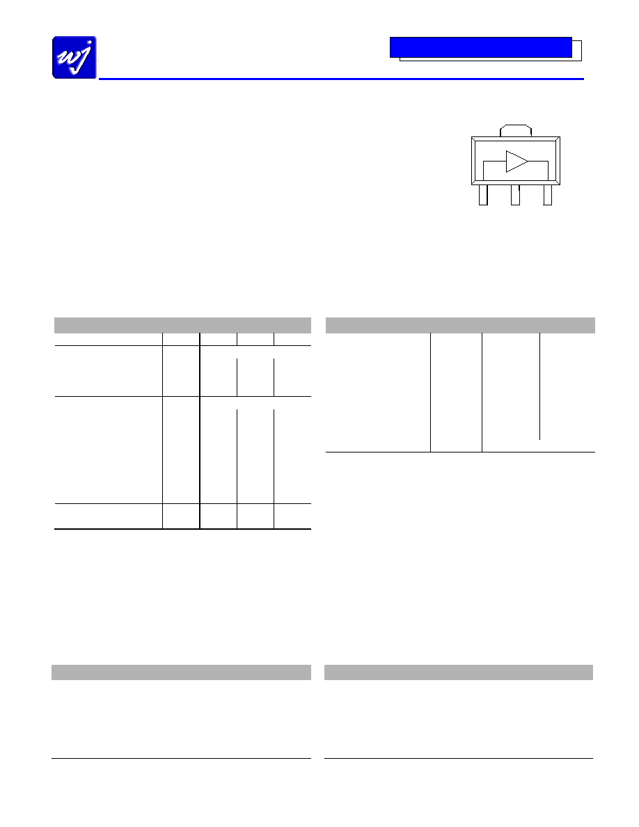
Functional Diagram
RF IN
GND
RF OUT
GND
1
2
3
4
ECG014B
Specifications
(1)
Parameters
Units Min
Typ Max
Operational Bandwidth
MHz
50
2000
Test Frequency
MHz
900
Gain dB
18.5
20.5
Output P1dB
dBm
+22
+23
Output OIP3
(2)
dBm
+38
+39
Test Frequency
MHz
1900
Gain dB
17
17.6
Input Return Loss
dB
17
Output Return Loss
dB
7.4
Output P1dB
dBm
+23
Output IP3
(2)
dBm
+36.5
+38
IS-95A Channel Power
@ -45 dBc ACPR, 1900 MHz
dBm +16
Noise Figure
dB
5.2
Operating Current Range
(3)
mA 85 100 135
Device Voltage
(4)
V
5
1. Test conditions unless otherwise noted: 25
∞C, Vsupply = +8V, in tuned application circuit with
Rbias = 30
.
2. 3OIP measured with two tones at an output power of +9 dBm/tone separated by 1 MHz. The
suppression on the largest IM3 product is used to calculate the 3OIP using a 2:1 rule. The tuned
application circuit is tuned for optimum ACPR performance. An improvement in OIP3 of 2 to 3
dB can be achieved for tuning for optimum OIP3 (with slightly degraded ACPR performance).
3. This corresponds to the quiescent current or operating current under small-signal conditions.
4. This device requires a minimum 7 V power supply through a dropping resistor. 8 V and 30 ohms
are recommended for proper operation. Operation of the device directly to a 5 V supply could lead
to thermal damage to the device.
Typical Performance
(5)
Parameters
Units
Typical
Frequency
MHz
900
1900
S21 ≠ Gain
dB
20.5
17.6
S11 ≠ Input R.L.
dB
-20
-17
S22 ≠ Output R.L.
dB
-9.5
-7.4
Output P1dB
Output IP3
(2)
dBm
dBm
+22.8
+39
+23
+38
IS-95A Channel Power
@ -45 dBc ACPR, 1900 MHz
dBm +17 +16
Noise Figure
dB
5
5.2
Supply Bias
+8 V @ 100 mA
5. Typical parameters reflect performance in a tuned application circuit: Supply Voltage = +8 V, I
cc
=
100 mA, +25
∞ C, Rbias = 30 .
Absolute Maximum Rating
Ordering Information
Parameters
Rating
Part No.
Description
Operating Case Temperature
-40 to +85
∞C
ECG014B
0.2 Watt, High Linearity InGaP HBT Amplifier
Storage Temperature
-65 to +150
∞C
ECG014B-PCB900
900 MHz Evaluation Board
RF Input Power (continuous)
+12 dBm
ECG014B-PCB1900
1900 MHz Evaluation Board
Device Voltage
+6 V
Device Current
150 mA
Device Power
1.5 W
Junction Temperature
+250
∞C
Operation of this device above any of these parameters may cause permanent damage.
.
Specifications and information are subject to change without notice
WJ Communications, Inc
∑
Phone 1-800-WJ1-4401
∑
FAX: 408-577-6621
∑
e-mail: sales@wj.com
∑
Web site: www.wj.com
August
2004
ECG014
0.2 Watt, High Linearity InGaP HBT Amplifier
Product Information
The Communications Edge
TM
Typical Device Data
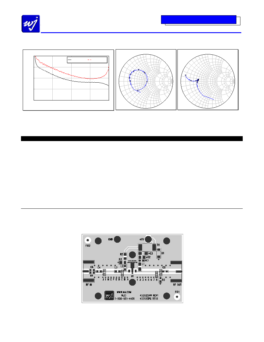
S-parameters (V
device
= +5V, I
cc
= 100 mA, 25
∞ C, unmatched 50 ohm system)
0
0.5
1
1.5
2
Frequency (GHz)
Gain / Maximum Stable Gain
10
15
20
25
30
Ga
in
(
d
B)
DB(|S[2,1]|)
DB(GMax)
0
1.
0
1.0
-1
.
0
1
0.0
10.0
-1
0.
0
5.
0
5.0
-5.
0
2.
0
2.
0
-2
.0
3.
0
3.
0
-3
.0
4.
0
4.0
-4
.0
0.
2
0.2
-0.
2
0.
4
0.
4
-0
.4
0.
6
0.
6
-0
.6
0.
8
0
.
8
-
0
.
8
S11
Swp Max
2.01283GHz
Swp Min
0.01483GHz
0
1.
0
1.
0
-1
.0
10
.0
10.0
-1
0.
0
5.
0
5.0
-5.
0
2.
0
2.
0
-2
.0
3.
0
3.
0
-3
.0
4.
0
4.
0
-4
.0
0.
2
0.2
-0.
2
0.
4
0.
4
-0
.4
0.
6
0.
6
-0
.6
0.
8
0
.
8
-
0
.
8
S22
Swp Max
2.01283GHz
Swp Min
0.01483GHz
Notes:
The gain for the unmatched device in 50 ohm system is shown as the trace in blue color. For a tuned circuit for a particular frequency, it is expected that
actual gain will be higher, up to the maximum stable gain. The maximum stable gain is shown in the dashed red line.
The impedance plots are shown from 50 ≠ 2500 MHz, with markers placed at 0.25 ≠ 2 GHz in 0.25 GHz increments.
S-Parameters (V
device
= +5 V, I
cc
= 100 mA, T = 25
∞ C, unmatched 50 ohm system, calibrated to device leads)
Freq (MHz)
S11 (dB)
S11 (ang)
S21 (dB)
S21 (ang)
S12 (dB)
S12 (ang)
S22 (dB)
S22 (ang)
50
-5.21 -158.20 27.34 141.96 -32.11 16.29 -6.58 -132.30
100 -4.92 -170.08 25.32 144.95 -31.61 9.45 -7.49 -157.02
200 -4.72 -177.73 24.15 138.50 -31.37 6.88 -7.96 -171.72
400 -4.31
173.22
22.43
118.30
-30.63 7.98 -8.46
178.73
600 -4.10
163.26
20.91
100.56
-30.32 5.52 -8.81
174.06
800 -4.19 152.57 19.68 85.04 -29.78 2.65 -9.07 171.40
1000 -4.63 140.41 18.82 69.98 -29.74 -2.18 -9.12 169.67
1200 -5.64 126.43 18.35 54.85 -29.31 -11.26 -8.95 170.98
1400 -7.84 109.08 18.13 38.12 -29.86 -26.72 -8.04 175.14
1600 -13.52 83.27 18.12 17.54 -31.16 -52.52 -6.16 179.09
1800 -19.89 -85.25 17.78 -7.75 -34.99 -105.12 -3.43 176.43
2000 -6.99 -131.98 16.44 -37.07 -34.48 161.53 -1.36 164.56
2200 -2.84 -160.75 14.09 -64.48 -29.33 106.22 -0.69 149.67
2400 -1.18 177.40 10.90 -86.11 -26.64 75.52 -0.93 136.25
2500 -0.78 167.87 9.28 -96.04 -25.96 66.16 -1.28 130.16
Device S-parameters are available for download off of the website at: http://www.wj.com
Application Circuit PC Board Layout
Circuit Board Material: .014" Getek, 4 - layer, 1 oz copper, Microstrip line details: width = .026", spacing = .026"
The silk screen markers `A', `B', `C', etc. and `1', `2', `3', etc. are used as placemarkers for the input and output tuning shunt capacitors.
The markers and vias are spaced in .050" increments.
C7/C8 are for 900 MHz matching circuits and C9/C12 are for 1900 MHz matching circuits.
C8
C7
C9
C12

.
Specifications and information are subject to change without notice
WJ Communications, Inc
∑
Phone 1-800-WJ1-4401
∑
FAX: 408-577-6621
∑
e-mail: sales@wj.com
∑
Web site: www.wj.com
August
2004
ECG014
0.2 Watt, High Linearity InGaP HBT Amplifier
Product Information
The Communications Edge
TM
900 MHz Application Circuit (ECG014B-PCB900)
Typical RF Performance at 25
∞C
Please see note 2 on page 1.
CAP
C=
ID=
56 pF
C4
CAP
C=
ID=
56 pF
C5
IND
L=
ID=
33 nH
L1
CAP
ID= C3
CAP
C=
ID=
0.8 pF
C8
RES
R=
ID=
390 Ohm
R2
RES
R=
ID=
220 Ohm
R3
IND
L=
ID=
33 nH
L2
RES
R=
ID=
30 Ohm
R1
CAP
C=
ID=
56 pF
C6
RES
R=
ID=
22 Ohm
R4
CAP
C=
ID=
56 pF
C1
CAP
C=
ID=
1000 pF
C2
CAP
C=
ID=
5.6 pF
C7
RES
R=
ID=
50 Ohm
R5
SUBCKT
PORT
Z=
P=
50 Ohm
1
PORT
Z=
P=
50 Ohm
2
8.2v zener
8v
ECG014 900 MHz
C = .1uF
C7 is placed at silkscreen marker `C' or center of component placed at 5.6 deg. @ 900 MHz away from pin 1. C8 is
placed at 22 deg. @ 900 MHz away from pin 3.
S21 vs. Frequency
16
18
20
22
24
840
860
880
900
920
940
Frequency (MHz)
S2
1
(
d
B
)
+25∞C
+85∞C
-40∞C
S11 vs. Frequency
-40
-35
-30
-25
-20
-15
-10
-5
0
840
860
880
900
920
940
Frequency (MHz)
S
11
(
dB
)
+25∞C
+85∞C
-40∞C
S22 vs. Frequency
-25
-20
-15
-10
-5
0
840
860
880
900
920
940
Frequency (MHz)
S
22
(
dB
)
+25∞C
+85∞C
-40∞C
Noise Figure vs. Frequency
0
2
4
6
8
840
860
880
900
920
940
Frequency (MHz)
NF
(
dB
)
+25∞C
+85∞C
-40∞C
P1 dB vs. Frequency
20
21
22
23
24
25
840
860
880
900
920
940
Frequency (MHz)
P1
d
B
(
dBm
)
+25∞C
+85∞C
-40∞C
ACPR vs. Channel Power
IS-95, 9 Ch. Fwd, ±885 KHz offset, 30 KHz Meas. BW, 900 MHz
-70
-65
-60
-55
-50
-45
-40
12
13
14
15
16
17
18
Output Channel Power (dBm)
ACP
R (
d
Bc
)
+25∞C
+85∞C
-40∞C
OIP3 vs. Frequency
+25∞C, +9 dBm / tone
30
32
34
36
38
40
42
840
860
880
900
920
940
Frequency (MHz)
OI
P
3
(
d
B
m
)
OIP3 vs. Temperature
Fre. = 900, 901 MHz, +9 dBm / tone
32
34
36
38
40
42
-40
-15
10
35
60
85
Temperature (∞C)
OI
P
3
(
d
B
m
)
OIP3 vs. Output Power
Freq. = 900, 901 MHz, +25∞C
32
34
36
38
40
42
6
7
8
9
10
11
12
13
14
Output Power (dBm)
OI
P
3
(
d
B
m
)
Frequency
900 MHz
S21 ≠ Gain
20.5 dB
S11 ≠ Input Return Loss
-20 dB
S22 ≠ Output Return Loss
-9.5 dB
Output P1dB
+22.8 dBm
Output IP3
(+9 dBm / tone, 1 MHz spacing)
+39 dBm
Channel Power
(@-45 dBc ACPR, IS-95 9 channels fwd)
+17 dBm
Noise Figure
5 dB
Device Voltage
+5 V
Quiescent Current
100 mA

.
Specifications and information are subject to change without notice
WJ Communications, Inc
∑
Phone 1-800-WJ1-4401
∑
FAX: 408-577-6621
∑
e-mail: sales@wj.com
∑
Web site: www.wj.com
August
2004
ECG014
0.2 Watt, High Linearity InGaP HBT Amplifier
Product Information
The Communications Edge
TM
1900 MHz Application Circuit (ECG014B-PCB1900)
Typical RF Performance at 25
∞C
Please see note 2 on page 1.
CAP
C=
ID=
56 pF
C4
CAP
C=
ID=
56 pF
C5
IND
L=
ID=
1 nH
L3
IND
L=
ID=
15 nH
L1
CAP
ID= C3
CAP
C=
ID=
1.5 pF
C7
CAP
C=
ID=
0.7 pF
C10
RES
R=
ID=
390 Ohm
R2
RES
R=
ID=
220 Ohm
R3
IND
L=
ID=
15 nH
L2
RES
R=
ID=
30 Ohm
R1
CAP
C=
ID=
56 pF
C6
RES
R=
ID=
22 Ohm
R4
CAP
C=
ID=
56 pF
C1
CAP
C=
ID=
1000 pF
C2
SUBCKT
PORT
Z=
P=
50 Ohm
1
PORT
Z=
P=
50 Ohm
2
8.2v zener
8v
ECG014 1.9GHz
C = .1uF
C9 placed at silkscreen marker `8" or center of component placed at 39 deg. @ 1900 MHz away from pin 1.
C12 is placed at silkscreen marker `I" or center of component placed at 43 deg. @ 1.9 GHz away from pin 1.
S21 vs. Frequency
0
5
10
15
20
25
1850 1870 1890 1910 1930 1950 1970 1990
Frequency (MHz)
S
21
(
dB
)
+25∞C
+85∞C
-40∞C
S11 vs. Frequency
-25
-20
-15
-10
-5
0
1850 1870 1890 1910 1930 1950 1970 1990
Frequency (MHz)
S
11
(
dB
)
+25∞C
+85∞C
-40∞C
S22 vs. Frequency
-12
-10
-8
-6
-4
-2
0
1850 1870 1890 1910 1930 1950 1970 1990
Frequency (MHz)
S2
2
(
dB
)
+25∞C
+85∞C
-40∞C
Noise Figure vs. Frequency
0
1
2
3
4
5
6
7
1850 1870 1890 1910 1930 1950 1970 1990
Frequency (MHz)
NF
(
dB
)
+25∞C
+85∞C
-40∞C
P1 dB vs. Frequency
15
17
19
21
23
25
1850 1870 1890 1910 1930 1950 1970 1990
Frequency (MHz)
P1
d
B
(
dB
m
)
+25∞C
+85∞C
-40∞C
ACPR vs. Channel Power
IS-95, 9 Ch. Fwd. ±885 KHz offset, 30 KHz Meas. BW, 1900 MHz
-70
-65
-60
-55
-50
-45
-40
-35
10
11
12
13
14
15
16
17
18
Output Power (dBm)
AC
P
R
(
dB
c
)
OIP3 vs. Frequency
+25∞C, +9 dBm / tone
32
34
36
38
40
42
1850 1870 1890 1910 1930 1950 1970 1990
Frequency (MHz)
OI
P
3
(
d
B
m
)
OIP3 vs. Temperature
freq. = 1900, 1901 MHz, +9 dBm / tone
32
34
36
38
40
42
-40
-15
10
35
60
85
Temperature (∞C)
OI
P
3
(
d
B
m
)
OIP3 vs. Output Power
Freq. = 1900, 1901 MHz, 25∞C
32
34
36
38
40
42
6
7
8
9
10
11
12
13
14
Output Power (dBm)
OI
P
3
(
d
B
m
)
Frequency
1900 MHz
S21 ≠ Gain
17.6 dB
S11 ≠ Input Return Loss
-17 dB
S22 ≠ Output Return Loss
-7.4 dB
Output P1dB
+23 dBm
Output IP3
(+9 dBm / tone, 1 MHz spacing)
+38 dBm
Channel Power
(@-45 dBc ACPR, IS-95 9 channels fwd)
+16 dBm
Noise Figure
5.2 dB
Device Voltage
+5 V
Quiescent Current
100 mA

.
Specifications and information are subject to change without notice
WJ Communications, Inc
∑
Phone 1-800-WJ1-4401
∑
FAX: 408-577-6621
∑
e-mail: sales@wj.com
∑
Web site: www.wj.com
August
2004
ECG014
0.2 Watt, High Linearity InGaP HBT Amplifier
Product Information
The Communications Edge
TM
Outline Drawing
Land Pattern
Thermal Specifications
Parameter
Rating
Operating Case Temperature
-40 to +85
∞ C
Thermal Resistance, Rth
(1)
128
∞ C / W
Junction Temperature, Tjc
(2)
149
∞ C
Notes:
1. The thermal resistance is referenced from the
junction-to-case at a case temperature of 85
∞ C.
2. This corresponds to the typical biasing condition of
+5V, 100 mA at an 85
∞ C case temperature. A
minimum MTTF of 1 million hours is achieved for
junction temperatures below 247
∞ C.
Product Marking
The component will be marked with an "E014"
designator with an alphanumeric lot code on the
top surface of the package.
Tape and reel specifications for this part are
located on the website in the "Application Notes"
section.
ESD / MSL Information
ESD Rating: Class 1B
Value:
Passes between 500 and 1000V
Test:
Human Body Model (HBM)
Standard:
JEDEC Standard JESD22-A114
MSL Rating: Level 3 at +235
∞ C convection reflow
Standard:
JEDEC Standard J-STD-020
Mounting Config. Notes
1. Ground / thermal vias are critical for the proper
performance of this device. Vias should use
a .35mm (#80 / .0135") diameter drill and have a
final plated thru diameter of .25 mm (.010").
2. Add as much copper as possible to inner and
outer layers near the part to ensure optimal
thermal performance.
3. Mounting screws can be added near the part to
fasten the board to a heatsink. Ensure that the
ground / thermal via region contacts the heatsink.
4. Do not put solder mask on the backside of the
PC board in the region where the board contacts
the heatsink.
5. RF trace width depends upon the PC board
material and construction.
6. Use 1 oz. Copper minimum.
7. All dimensions are in millimeters (inches).
Angles are in degrees.
MTTF vs. GND Tab Temperature
100
1000
10000
100000
60
70
80
90
100
110
120
Tab Temperature (∞C)