 | –≠–ª–µ–∫—Ç—Ä–æ–Ω–Ω—ã–π –∫–æ–º–ø–æ–Ω–µ–Ω—Ç: ECG015B-G | –°–∫–∞—á–∞—Ç—å:  PDF PDF  ZIP ZIP |

Specifications and information are subject to change without notice
WJ Communications, Inc
∑
Phone 1-800-WJ1-4401
∑
FAX: 408-577-6621
∑
e-mail: sales@wj.com
∑
Web site: www.wj.com
September
2004
ECG015
º Watt, High Linearity InGaP HBT Amplifier
Product Information
The Communications Edge
TM
Product Features
∑
1800 ≠ 2500 MHz
∑
+24 dBm P1dB
∑
+41 dBm OIP3
∑
15 dB Gain
∑
5 dB Noise Figure
∑
Single Positive Supply (+8V)
∑
Available in a lead-free / green
SOT-89 Package Style
Applications
∑
Mobile Infrastructure
∑
W-LAN / ISM
∑
RFID
∑
Defense / Homeland Security
∑
Fixed Wireless
Product Description
The ECG015 is a high dynamic range driver amplifier in a
low-cost surface mount package. The InGaP/GaAs HBT is
able to achieve performance over a broad range with +41
dBm OIP3 and +24 dBm of compressed 1dB power and is
housed in a lead-free/green/RoHS-compliant SOT-89 SMT
package. All devices are 100% RF and DC tested.
The product is targeted for use as a gain block/driver
amplifier for various current and next generation wireless
technologies such as GPRS, UMTS and WCDMA, where
high linearity and medium power is required. In addition,
the ECG015 will work for numerous other applications
within the 1800 to 2500 MHz frequency range.
Functional Diagram
RF IN
GND
RF OUT
GND
1
2
3
4
ECG015B / ECG015B-G
Specifications
(1)
Parameter
Units Min
Typ
Max
Operational
Bandwidth
MHz
1800 2500
Test Frequency
MHz
2140
Gain dB
13.5
15
Input
Return
Loss
dB 17
Output Return Loss
dB
10
Output P1dB
dBm
+22
+24
Output IP3
(2)
dBm
+37.5
+41
Noise Figure
dB
5
Device Voltage
V
5
Device Current
mA
85
100
135
1. Test conditions unless otherwise noted: 25
∞C, Vsupply = +8V, in tuned application circuit with
Rbias = 30
.
2. 3OIP measured with two tones at an output power of +9Bm/tone separated by 1 MHz. The
suppression on the largest IM3 product is used to calculate the 3OIP using a 2:1 rule.
Absolute Maximum Rating
Parameter
Rating
Operating Case Temperature
-40 to +85
∞C
Storage Temperature
-55 to +125
∞C
Device Current
180 mA
RF Input Power (continuous)
+15 dBm
Junction Temperature
+250
∞C
Operation of this device above any of these parameters may cause permanent damage.
Typical Performance
(3)
Parameter
Units
Typical
Frequency
MHz 1900 2140 2450
S21
dB 21 15 14
S11
dB -15 -17 -19
S22
dB -10 -10 -10
Output
P1dB dBm +24 +24 +23
Output IP3
(2)
dBm +41 +41 +42
Noise
Figure dB 5 5 5
3. Typical parameters reflect performance in a tuned application circuit: Supply Voltage = +8 V, I
cc
=
100 mA, +25
∞ C, Rbias = 30 .
Ordering Information
Part No.
Description
ECG015B
0.2 Watt, High Linearity InGaP HBT Amplifier
(leaded SOT-89 Pkg)
ECG015B-G
0.2 Watt, High Linearity InGaP HBT Amplifier
(lead-free/green/RoHS-compliant SOT-89 Pkg)
ECG015B-PCB1900 1900 MHz Fully Assembled Eval. Board
ECG015B-PCB2140 2140 MHz Fully Assembled Eval. Board

Specifications and information are subject to change without notice
WJ Communications, Inc
∑
Phone 1-800-WJ1-4401
∑
FAX: 408-577-6621
∑
e-mail: sales@wj.com
∑
Web site: www.wj.com
September
2004
ECG015
º Watt, High Linearity InGaP HBT Amplifier
Product Information
The Communications Edge
TM
Typical Device Data
S-parameters (V
device
= +5V, I
cc
= 100 mA, 25
∞ C, unmatched 50 ohm system)
1.8
1.9
2
2.1
2.2
2.3
2.4
2.5
Frequency (GHz)
Gain / Maximum Stable Gain
10
15
20
25
30
Ga
in
(
d
B)
DB(|S[2,1]|)
DB(GMax)
0
1.
0
1.0
-1
.
0
1
0.0
10.0
-1
0.
0
5.
0
5.0
-5.
0
2.
0
2.
0
-2
.0
3.
0
3.
0
-3
.0
4.
0
4.0
-4
.0
0.
2
0.2
-0.
2
0.
4
0.
4
-0
.4
0.
6
0.
6
-0
.6
0.
8
0
.
8
-
0
.
8
S11
Swp Max
2.50123GHz
Swp Min
1.79083GHz
0
1.
0
1.
0
-1
.0
10
.0
10.0
-1
0.
0
5.
0
5.0
-5.
0
2.
0
2.
0
-2
.0
3.
0
3.
0
-3
.0
4.
0
4.
0
-4
.0
0.
2
0.2
-0.
2
0.
4
0.
4
-0
.4
0.
6
0.
6
-0
.6
0.
8
0
.
8
-
0
.
8
S22
Swp Max
2.50123GHz
Swp Min
1.79083GHz
Notes:
The gain for the unmatched device in 50 ohm system is shown as the trace in blue color. For a tuned circuit for a particular frequency, it is expected that
actual gain will be higher, up to the maximum stable gain. The maximum stable gain is shown in the dashed red line.
The impedance plots are shown from 1800 ≠ 2500 MHz, with markers placed at 1.8 ≠ 2.5 GHz in 0.1 GHz increments.
S-Parameters (V
device
= +5 V, I
cc
= 100 mA, T = 25
∞ C, unmatched 50 ohm system, calibrated to device leads)
Freq (MHz)
S11 (dB)
S11 (ang)
S21 (dB)
S21 (ang)
S12 (dB)
S12 (ang)
S22 (dB)
S22 (ang)
1800 -6.70 80.76 15.90 24.47 -28.55 -25.74 -5.34 156.39
1900 -7.55 68.30 15.77 16.51 -28.96 -32.29 -4.96 156.21
2000 -8.60 53.47 15.66 7.76 -30.14 -38.84 -4.56 155.58
2100 -9.85 35.06 15.53 -1.19 -31.49 -45.79 -4.12 155.07
2200 -11.07 10.07 15.40 -10.90 -33.04 -59.63 -3.67 153.49
2300 -11.69 -21.71 15.08 -20.90 -36.28 -78.21 -3.20 150.85
2400 -10.87 -56.13 14.67 -31.83 -40.69 -106.46 -2.80 147.22
2500 -9.15 -86.03 14.14 -43.53 -42.21 163.73 -2.44 142.35
Device S-parameters are available for download off of the website at: http://www.wj.com
Application Circuit PC Board Layout
Circuit Board Material: .014" Getek, 4 - layer, 1 oz copper, Microstrip line details: width = .026", spacing = .026"
The silk screen markers `A', `B', `C', etc. and `1', `2', `3', etc. are used as placemarkers for the input and output tuning shunt
capacitors. The markers and vias are spaced in .050" increments.

Specifications and information are subject to change without notice
WJ Communications, Inc
∑
Phone 1-800-WJ1-4401
∑
FAX: 408-577-6621
∑
e-mail: sales@wj.com
∑
Web site: www.wj.com
September
2004
ECG015
º Watt, High Linearity InGaP HBT Amplifier
Product Information
The Communications Edge
TM
Typical Device RF Performance
Supply Bias = +8 V, R
bias
= 30
, I
cc
= 100 mA
1. Test conditions: T = 25∫ C, Supply Voltage = +8 V, Device Voltage = 5.0 V, Rbias = 30
, Icc = 100 mA typical, 50 System.
2. 3OIP measured with two tones at an output power of +11 dBm/tone separated by 1 MHz. The suppression on the largest IM3 product is used to calculate the 3OIP using a 2:1 rule.
3. Data is shown as device performance only. Actual implementation for the desired frequency band will be determined by external components shown in the application circuit.
Ssg & P1dB vs.
Temperature @ 1.96GHz
12
14
16
18
20
22
24
-40∞C
25∞C
85∞C
Ssg
OIP3
P1dB
ACPR1 vs. Pout
at 1.9GHz (IS95 9 Ch. Fwd)
0
10
20
30
40
50
60
70
11
13
15
17
Average power out(dBm)
dBc
85∞C
-40∞C
25∞C
P1dB vs. Frequency
22
22.5
23
23.5
24
24.5
1.96GHz
2.14GHz
2.45GHz
dBm
ACPR1vs. Pout at 2.14GHz
(IS95 9 Ch Fwd)
0
10
20
30
40
50
60
70
11
13
15
17
Average power out(dBm)
dBc
25∞C
-40∞C
85∞C
Icc vs. Vde
0
20
40
60
80
100
120
140
4.5
4.7
4.9
5.1
5.3
Vde
I
cc
(
mA
)
25∞C
Ssg, OIP3 and P1dB vs.
Temperature at 2.45GHz
38
40
42
44
-40∞C
25∞C
85∞C
12
16
20
24
OIP3
Ssg
P1dB

Specifications and information are subject to change without notice
WJ Communications, Inc
∑
Phone 1-800-WJ1-4401
∑
FAX: 408-577-6621
∑
e-mail: sales@wj.com
∑
Web site: www.wj.com
September
2004
ECG015
º Watt, High Linearity InGaP HBT Amplifier
Product Information
The Communications Edge
TM
ECG015B (SOT-89 Package) Mechanical Information
This package may contain lead-bearing materials.
Outline Drawing
Land Pattern
Thermal Specifications
Parameter
Rating
Operating Case Temperature
-40 to +85
∞ C
Thermal Resistance, Rth
(1)
128
∞ C / W
Junction Temperature, Tjc
(2)
149
∞ C
Notes:
1. The thermal resistance is referenced from the
junction-to-case at a case temperature of 85
∞ C.
2. This corresponds to the typical biasing condition of
+5V, 100 mA at an 85
∞ C case temperature. A
minimum MTTF of 1 million hours is achieved for
junction temperatures below 247
∞ C.
Product Marking
The component will be marked with an "E015"
designator with an alphanumeric lot code on the
top surface of the package.
Tape and reel specifications for this part are
located on the website in the "Application Notes"
section.
ESD / MSL Information
ESD Rating: Class 1B
Value: Passes at between 500 and 1000V
Test: Human Body Model (HBM)
Standard: JEDEC Standard JESD22-A114
MSL Rating: Level 3 at +240
∞C convection reflow
Standard: JEDEC Standard J-STD-020
Mounting Config. Notes
1. Ground / thermal vias are critical for the proper
performance of this device. Vias should use a .35mm (#80
/ .0135") diameter drill and have a final plated thru
diameter of .25 mm (.010").
2. Add as much copper as possible to inner and outer layers
near the part to ensure optimal thermal performance.
3. Mounting screws can be added near the part to fasten the
board to a heatsink. Ensure that the ground / thermal via
region contacts the heatsink.
4. Do not put solder mask on the backside of the PC board in
the region where the board contacts the heatsink.
5. RF trace width depends upon the PC board material and
construction.
6. Use 1 oz. Copper minimum.
7. All dimensions are in millimeters (inches). Angles are in
degrees.
MTTF vs. GND Tab Temperature
100
1000
10000
100000
60
70
80
90
100
110
120
Tab Temperature (∞C)
Specifications and information are subject to change without notice
WJ Communications, Inc
∑
Phone 1-800-WJ1-4401
∑
FAX: 408-577-6621
∑
e-mail: sales@wj.com
∑
Web site: www.wj.com
September
2004
ECG015
º Watt, High Linearity InGaP HBT Amplifier
Product Information
The Communications Edge
TM
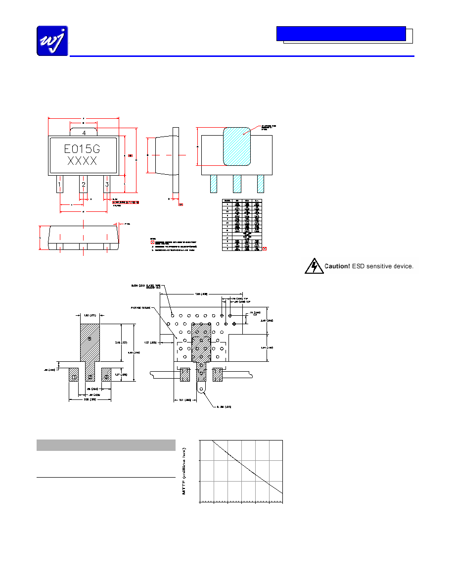
ECG015B (Green / Lead-free SOT-89 Package) Mechanical Information
This package is lead-free/Green/RoHS-compliant. It is compatible with both lead-free (maximum 260
∞C reflow temperature) and leaded
(maximum 245
∞C reflow temperature) soldering processes.
Outline Drawing
Land Pattern
Thermal Specifications
Parameter
Rating
Operating Case Temperature
-40 to +85
∞ C
Thermal Resistance, Rth
(1)
128
∞ C / W
Junction Temperature, Tjc
(2)
149
∞ C
Notes:
1. The thermal resistance is referenced from the
junction-to-case at a case temperature of 85
∞ C.
2. This corresponds to the typical biasing condition of
+5V, 100 mA at an 85
∞ C case temperature. A
minimum MTTF of 1 million hours is achieved for
junction temperatures below 247
∞ C.
Product Marking
The component will be marked with an "E015G"
designator with an alphanumeric lot code on the
top surface of the package.
Tape and reel specifications for this part are
located on the website in the "Application Notes"
section.
ESD / MSL Information
ESD Rating: Class 1B
Value: Passes at between 500 and 1000V
Test: Human Body Model (HBM)
Standard: JEDEC Standard JESD22-A114
MSL Rating: Level 3 at +260
∞C convection reflow
Standard: JEDEC Standard J-STD-020
Mounting Config. Notes
1. Ground / thermal vias are critical for the proper
performance of this device. Vias should use a .35mm (#80
/ .0135") diameter drill and have a final plated thru
diameter of .25 mm (.010").
2. Add as much copper as possible to inner and outer layers
near the part to ensure optimal thermal performance.
3. Mounting screws can be added near the part to fasten the
board to a heatsink. Ensure that the ground / thermal via
region contacts the heatsink.
4. Do not put solder mask on the backside of the PC board in
the region where the board contacts the heatsink.
5. RF trace width depends upon the PC board material and
construction.
6. Use 1 oz. Copper minimum.
7. All dimensions are in millimeters (inches). Angles are in
degrees.
MTTF vs. GND Tab Temperature
100
1000
10000
100000
60
70
80
90
100
110
120
Tab Temperature (∞C)