Document Outline
- WAN-0143
- ADA and MASK Timing on WM9712
- INTRODUCTION
- WM9712 SETUP
- MASK FUNCTION
- INTERFACE TIMING
- ALTERNATIVE MASK FUNCTION
- ADA TIMING
- SUMMARY
- APPLICATION SUPPORT
- IMPORTANT NOTICE
- ADDRESS

w
WAN-0143
ADA and MASK Timing on WM9712
WOLFSON MICROELECTRONICS plc
www.wolfsonmicro.com
March 2004, Rev 1.0.
Copyright
2004 Wolfson Microelectronics plc
INTRODUCTION
This applications note has been created to detail the timing of the MASK and ADA (ADC Data
Available) signals on the WM9712 device. This applications note should be used in conjunction with
the latest WM9712 datasheet.
The WM9712 has many additional functions to aid the design of portable applications. Pin 47 of the
device can be configured for either MASK input, ADA output or standard GPIO functionality. The
MASK function can be used to pause and control auxiliary ADC conversions. The ADA function can
be used to indicate when data becomes available from the auxiliary ADC. The timing associated
with both signals is detailed in the following sections of this document.
WM9712 SETUP
The WM9712 device must be configured to setup the function of pin 47. The three possible setups
are:
�
MASK Input Function
�
ADA
Function
�
General
GPIO
To set the device into one of the three above modes the following configurations should be used.
PIN 47 MODE
REGISTER 56H BIT 4 SETTING
(GPIO FUNCTION SELECT)
REGISTER 4CH BIT 4 SETTING
(PIN DEFINED AS INPUT OR OUTPUT)
MASK 1 1
(Input)
ADA 1
0
(Output)
GPIO
0
1 or 0 (GPIO can be Input or Output)
Table 1 WM9712 Pin 47 Configuration
MASK FUNCTION
Sources of glitch noise, such as the signals driving an LCD display, may feed through to the
touchscreen plates and affect measurement accuracy. In order to minimise this effect, a signal may
be applied to MASK (pin 47) to delay or synchronise the sampling of any input to the ADC. The effect
of the MASK signal depends on the MSK[1-0] bits of register 78h, as described below.
MSK[1-0]
EFFECT OF SIGNAL ON MASK PIN
00
MASK has no effect on conversions GPIO input disabled (default)
01
Static; `hi' on MASK pin stops conversions, `lo' has no effect.
10
Edge triggered; rising or falling edge on MASK pin delays conversions
by an amount set in the DEL[3-0] register. Conversions are asynchronous to
the MASK signal.
11
Synchronous mode; conversions wait until rising or falling edge on MASK
initiates cycle; screen starts to be driven when the edge arrives, the
conversion sample being taken a period set by DEL[3-0] after the edge.
Table 2 Controlling the MASK Feature
WAN_0143
w
Rev 1.0 March 2004
2
The delay described in Table 2 refers to the length of time delay there will be from the edge of the
MASK signal to the start of the next auxiliary ADC conversion. This delay is defined as shown in
Table 3 and Table 4 below.
REGISTER
ADDRESS
BIT LABEL
DEFAULT
DESCRIPTION
76h
7:4
DEL
0000
(1 frame)
Delay Time
Table 3 Delay Time Control (1)
DEL DELAY
(AC-LINK FRAMES)
DELAY
(TIME)
0000 1
20.8
�
s
0001 2
41.7
�
s
0010 4
83.3
�
s
0011 8
167
�
s
0100 16
333
�
s
0101 32
667
�
s
0110 48
1ms
0111 64 1.33ms
1000 96
2ms
1001 128 2.67ms
1010 160 3.33ms
1011 192
4ms
1100 224 4.67ms
1101 256 5.33ms
1110 288
6ms
1111
No delay, switch matrix always on
Table 4 Delay Time Control (2)
The delay associated to MASK is the same as the settling delay associated with the actual auxiliary
ADC measurement.
For example, when MODE is Edge triggered, an edge on the MASK input will cause the next auxiliary
ADC measurement to be delayed by the value set in register 76h. After this delay for MASK the
auxiliary ADC conversion will be started.
Figure 1 details the timing associated with the delay set to 2 frames for each of the active MASK
modes.
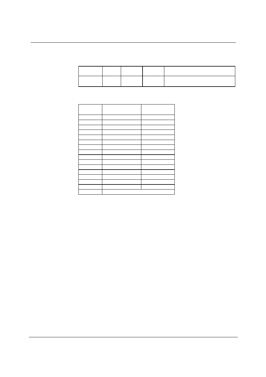
With MASK = 11, a conversion will be commanded and triggered by an edge of the MASK signal.
The delay from MASK edge to conversion is set by the DEL register setting. The delay is started on
the first SYNC pulse after an edge is detected on MASK (see figure 2 for further details).
With MASK = 10, a previously commanded conversion is paused by a delay reflected in the DEL
register setting.
With MASK = 01, any commanded conversions will be delayed while the MASK signal is HIGH.
Once the MASK signal returns low normal operation will resume.

WAN_0143
w
Rev 1.0 March 2004
3
INTERFACE TIMING
MASK
Frames
(SYNC)
AUXADC Conversion
(MASK = 11)
AUXADC Conversion
(MASK = 10)
AUXADC Conversion
(MASK = 01)
Conv
Delay
Conv
Conv
Conv
Conv
Conv
t
DEL
t
DEL
t
DEL
t
DEL
Delay
Delay
Conv
Delay
Conv
Delay
Conv
Delay
Conv
Delay
Figure 1 MASK Delay Timings (t
DEL
= 2 frames)
PARAMETER SYMBOL
MIN
TYP
MAX
UNIT
Frame Delay set by register 76h
t
DEL
0
288
frames
MASK
BCLK
SYNC
t
SETUP
t
SETUP
t
HOLD
t
HOLD
Figure 2 MASK Delay Timings
PARAMETER SYMBOL
MIN
TYP
MAX
UNIT
Setup time from MASK edge to SYNC
1
t
SETUP
162.8
ns
Hold time of MASK level from SYNC
rising edge.
t
HOLD
81.4
ns
Note:
1.
There must be at least two BCLK's between the rising edge of MASK and the rising edge of SYNC. Therefore, once MASK is
high there must be at least two BCLK rising edges prior to the SYNC pulse.
WAN_0143
w
Rev 1.0 March 2004
4
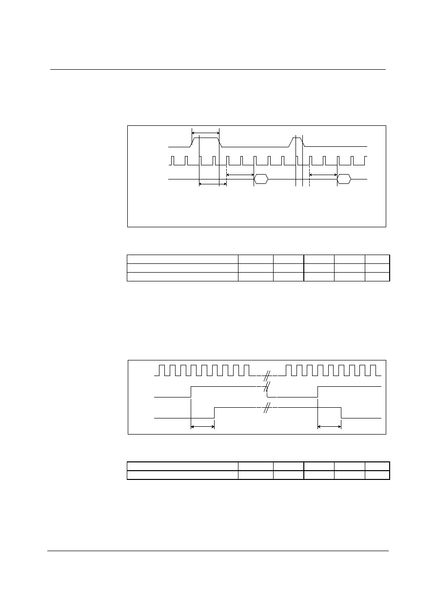
ALTERNATIVE MASK FUNCTION
When MASK = 11, synchronous mode, conversions are commanded on the rising and falling edges
of MASK input signal. However, there is an alternative operation which allows a pulse to be applied
to the MASK pin resulting in only one conversion taking place. In this setup the edges of the pulse
are too close together to allow two separate conversions to be commanded. Figure 3 details this
operation and the timing associated.
MASK
Frames
(SYNC)
AUXADC Conversion
(MASK = 11)
Conv
t
DEL
t
PULSE
t
DEL
Conv
t
DEL
Figure 3 MASK PULSE delay timings (t
DEL
= 2 frames)
PARAMETER SYMBOL
MIN
TYP
MAX
UNIT
MASK Pulse Width
t
PULSE
100ns
<
t
DEL
ns
Frame Delay set by register 76h
t
DEL
0 288
frames
ADA TIMING
Whenever data becomes available from the touchpanel ADC, the internal ADA signal goes high and
remains high until the data has been read from register 7Ah (if SLEN = 0) or until it has been sent out
on an AC-Link slot (if SLEN = 1).
If ADA is configured to be output on pin 47 the timing associated with this signal will be as follows.
BCLK
SYNC
ADA
t
ADA
t
ADA
Figure 4 ADA Timings
PARAMETER SYMBOL
MIN
TYP
MAX
UNIT
Delay from SYNC to ADA
t
ADA
200ns
ns

WAN_0143
w
Rev 1.0 March 2004
5
SUMMARY
Pin 47 of the WM9712 has three possible functions which are:
�
MASK
input,
�
ADA output or
�
General GPIO.
The modes and timings associated with MASK and ADA are detailed in this document. Further
information on these functions and the GPIO operation is detailed in the WM9712 datasheet.
APPLICATION SUPPORT
If you require more information or require technical support please contact Wolfson Microelectronics
Applications group through the following channels:
Email:
apps@wolfsonmicro.com
Telephone:
+44 (0)131 272 7070
Fax:
+44 (0)131 272 7001
Mail:
Applications at the address on last page.
or contact your local Wolfson representative.
Additional information may be made available from time to time on our web site at
http://www.wolfsonmicro.com

WAN_0143
w
Rev 1.0 March 2004
6
IMPORTANT NOTICE
Wolfson Microelectronics plc (WM) reserve the right to make changes to their products or to discontinue any product or service
without notice, and advise customers to obtain the latest version of relevant information to verify, before placing orders, that
information being relied on is current. All products are sold subject to the WM terms and conditions of sale supplied at the time of
order acknowledgement, including those pertaining to warranty, patent infringement, and limitation of liability.
WM warrants performance of its products to the specifications applicable at the time of sale in accordance with WM's standard
warranty. Testing and other quality control techniques are utilised to the extent WM deems necessary to support this warranty.
Specific testing of all parameters of each device is not necessarily performed, except those mandated by government
requirements.
In order to minimise risks associated with customer applications, adequate design and operating safeguards must be used by the
customer to minimise inherent or procedural hazards. Wolfson products are not authorised for use as critical components in life
support devices or systems without the express written approval of an officer of the company. Life support devices or systems are
devices or systems that are intended for surgical implant into the body, or support or sustain life, and whose failure to perform when
properly used in accordance with instructions for use provided, can be reasonably expected to result in a significant injury to the
user. A critical component is any component of a life support device or system whose failure to perform can be reasonably
expected to cause the failure of the life support device or system, or to affect its safety or effectiveness.
WM assumes no liability for applications assistance or customer product design. WM does not warrant or represent that any
license, either express or implied, is granted under any patent right, copyright, mask work right, or other intellectual property right of
WM covering or relating to any combination, machine, or process in which such products or services might be or are used. WM's
publication of information regarding any third party's products or services does not constitute WM's approval, license, warranty or
endorsement thereof.
Reproduction of information from the WM web site or datasheets is permissible only if reproduction is without alteration and is
accompanied by all associated warranties, conditions, limitations and notices. Representation or reproduction of this information
with alteration voids all warranties provided for an associated WM product or service, is an unfair and deceptive business practice,
and WM is not responsible nor liable for any such use.
Resale of WM's products or services with statements different from or beyond the parameters stated by WM for that product or
service voids all express and any implied warranties for the associated WM product or service, is an unfair and deceptive business
practice, and WM is not responsible nor liable for any such use.
ADDRESS:
Wolfson Microelectronics plc
Westfield House
26 Westfield Road
Edinburgh
EH11 2QW
Tel :: +44 (0)131 272 7000
Fax :: +44 (0)131 272 7001
Email :: apps@wolfsonmicro.com