 | –≠–ª–µ–∫—Ç—Ä–æ–Ω–Ω—ã–π –∫–æ–º–ø–æ–Ω–µ–Ω—Ç: WM2627C | –°–∫–∞—á–∞—Ç—å:  PDF PDF  ZIP ZIP |
Document Outline
- WM2627
- Quad 8-Bit Serial Input Voltage Output DAC
- Production Data, April 2001, Rev 1.0
- FEATURES
- DESCRIPTION
- APPLICATIONS
- ORDERING INFORMATION
- BLOCK DIAGRAM
- TYPICAL PERFORMANCE
- PIN CONFIGURATION
- PIN DESCRIPTION
- ABSOLUTE MAXIMUM RATINGS
- RECOMMENDED OPERATING CONDITIONS
- ELECTRICAL CHARACTERISTICS
- SERIAL INTERFACE
- TYPICAL PERFORMANCE GRAPHS
- DEVICE DESCRIPTION
- GENERAL FUNCTION
- HARDWARE CONFIGURATION OPTIONS
- SERIAL INTERFACE
- SOFTWARE CONFIGURATION OPTIONS
- APPLICATIONS INFORMATION
- LINEARITY, OFFSET, AND GAIN ERROR
- POWER SUPPLY DECOUPLING AND GROUNDING
- PACKAGE DIMENSIONS
WM2627
Quad 8-Bit Serial Input Voltage Output DAC
Production Data, April 2001, Rev 1.0
WOLFSON MICROELECTRONICS LTD
Lutton Court, Bernard Terrace, Edinburgh, EH8 9NX, UK
Tel: +44 (0) 131 667 9386
Fax: +44 (0) 131 667 5176
Email: sales@wolfson.co.uk
www.wolfsonmicro.com
Production Data Datasheets contain final
specifications current on publication date.
Supply of products conforms to Wolfson
Microelectronics' Terms and Conditions.
2001 Wolfson Microelectronics Ltd
.
FEATURES
∑
Four 8-bit voltage output DACs
∑
Dual 2.7V to 5.5V supply (separate digital and analogue
supplies)
∑
DNL
±
0.03 LSB, INL
±
0.3 LSB typical
∑
Low power consumption:
-
3mW, slow mode - 3V supply
-
9mW, fast mode - 3V supply
∑
DSP and microprocessor compatible serial interface
∑
Programmable settling time of 2.5
µ
s or 8.5
µ
s typical
APPLICATIONS
∑
Battery powered test instruments
∑
Digital offset and gain adjustment
∑
Battery operated/remote industrial controls
∑
Machine and motion control devices
∑
Wireless telephone and communication systems
∑
Arbitrary waveform generation
∑
Robotics
ORDERING INFORMATION
DEVICE
TEMP. RANGE
PACKAGE
WM2627CDT
0∞ to 70∞C
16-pin TSSOP
WM2627IDT
-40∞ to 85∞C
16-pin TSSOP
DESCRIPTION
The WM2627 is a quadruple 8-bit voltage output, resistor string,
digital-to-analogue converter. Each DAC can be individually
powered down under software control. A hardware controlled
mode is provided that powers down all DACs. Power down
reduces current consumption to 1
µ
A.
The device has been designed to interface efficiently to industry
standard microprocessors and DSPs. It is programmed with a
16-bit serial word comprising of a DAC address, individual DAC
control bits and an 8-bit value.
The WM2627 has provision for two supplies: one supply for the
serial interface (DVDD, DGND), and one for the DACs,
reference buffers and output buffers (AVDD, AGND). This
enables a typical application where the device can be controlled
via a microprocessor operating on a 3V supply, with the DACs
operating on a 5V supply. Alternatively, the supplies can be tied
together in a single supply application.
Excellent performance is delivered with a typical DNL of
±
0.03
LSB. The settling time of the DAC is programmable to allow the
designer to optimize speed versus power dissipation. The
output stage is buffered by a x2 gain near rail-to-rail amplifier,
which features a Class AB output stage. DACs A and B can
have a different reference voltage to DACs C and D.
The device is available in a 16-pin TSSOP package.
Commercial temperature (0
∞
to 70
∞
C) and Industrial
temperature (-40
∞
to 85
∞
C) variants are supported.
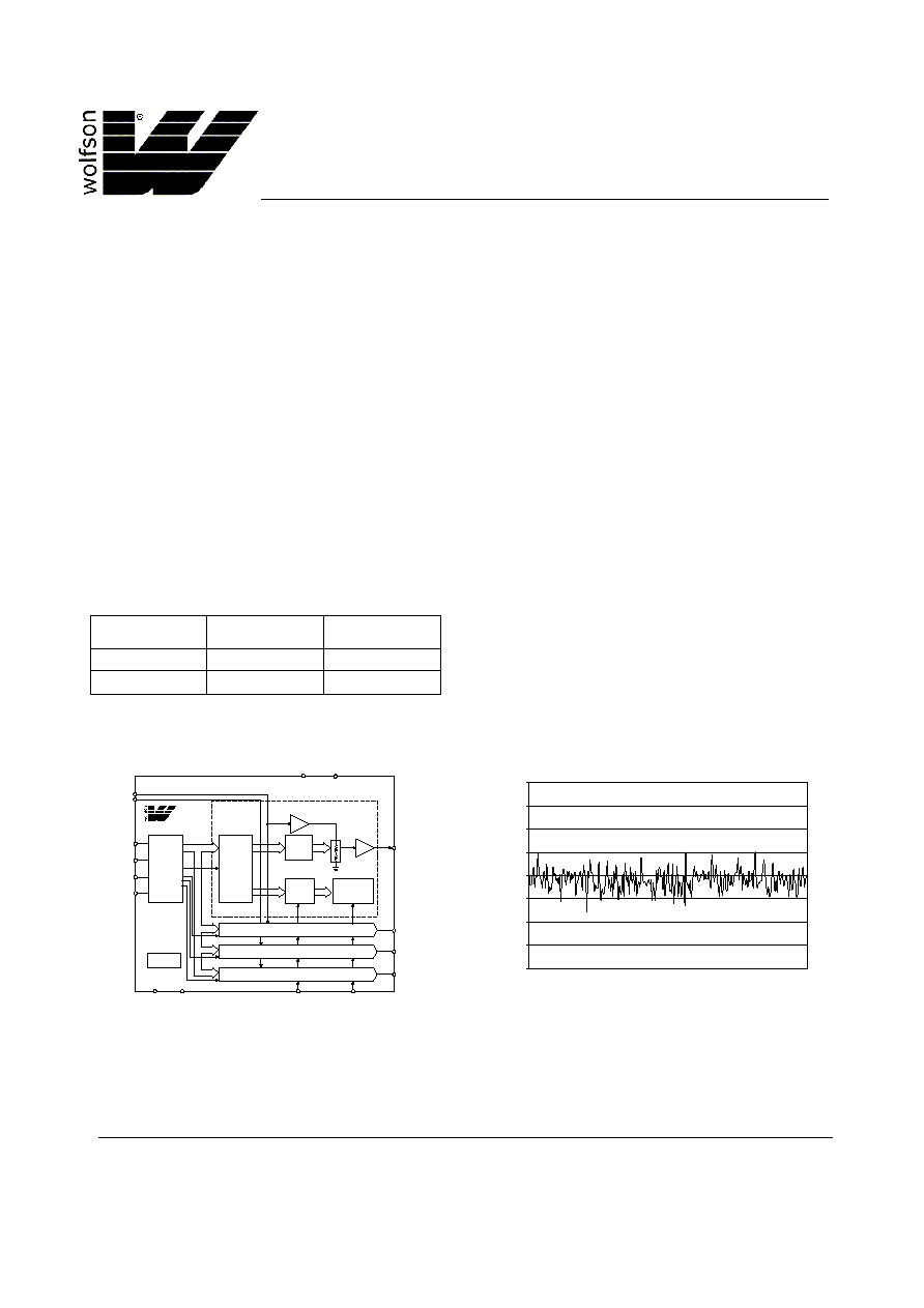
BLOCK DIAGRAM
TYPICAL PERFORMANCE
(11) OUTD
(12) OUTC
(13) OUTB
(14) OUTA
10-BIT
DATA AND
CONTROL
HOLDING
LATCH
8-BIT
DAC
LATCH
16-BIT
SHIFT
REGISTER
AND
CONTROL
LOGIC
REFINAB (15)
POWER-ON
RESET
DIN (4)
FS (7)
SCLK (5)
NCS (6)
(9)
AGND
(8)
DGND
(3)
NLDAC
(2)
NPD
AVDD
(16)
DVDD
(1)
X2
DAC A
DAC C
DAC D
POWERDOWN/
SPEED
CONTROL
WM2627
2-BIT
CONTROL
LATCH
REFINCD (10)
DAC B
X1
DAC
OUTPUT
BUFFER
data
REFERENCE
INPUT BUFFER
AVDD = DVDD = 5V, VREF = 2.048V, Slow Mode
-0.04
-0.03
-0.02
-0.01
0
0.01
0.02
0.03
0.04
0
32
64
96
128
160
192
224
256
DIGITAL CODE
Di
f
f
e
r
e
nt
i
a
l
Non-
Li
near
i
t
y (
L
SBs)
WM2627
Production Data
WOLFSON MICROELECTRONICS LTD
PD Rev 1.0 April 2001
2
PIN CONFIGURATION
12
11
10
16
15
14
13
5
6
7
1
2
3
4
REFINCD
OUTD
OUTC
OUTB
OUTA
AVDD
REFINAB
FS
NCS
SCLK
DIN
NLDAC
DVDD
NPD
8
DGND
9
AGND
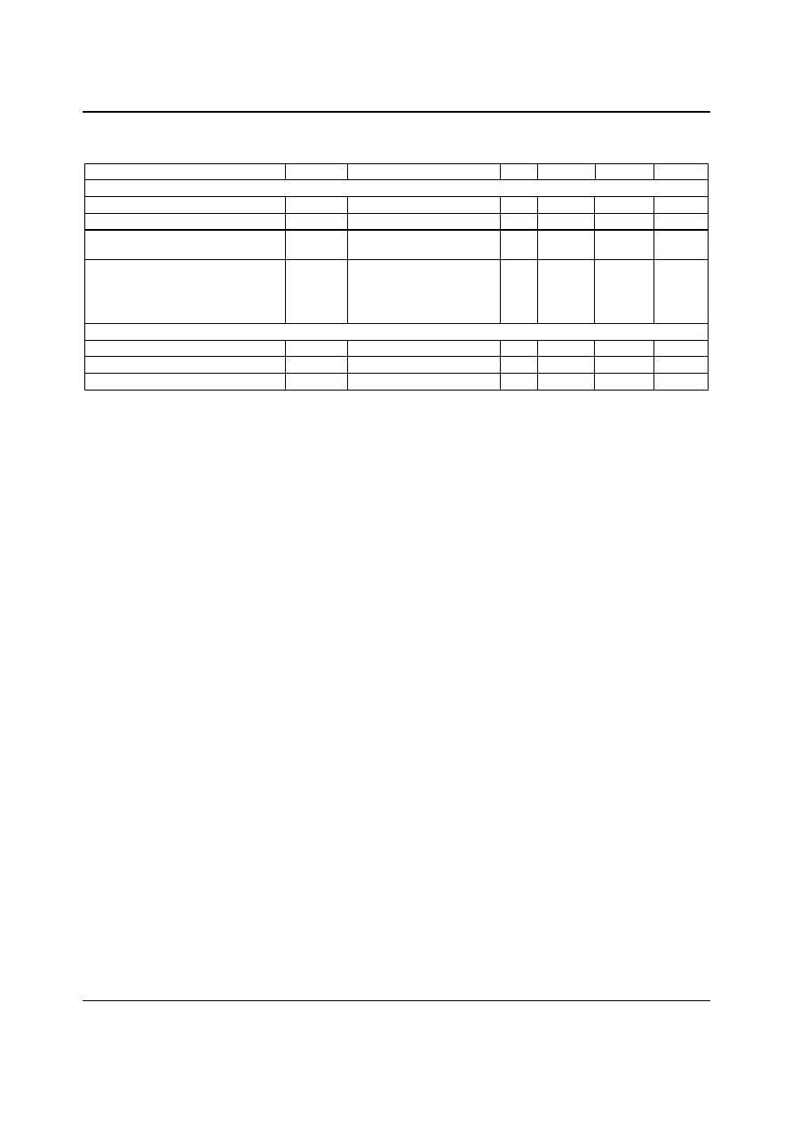
PIN DESCRIPTION
PIN NO
NAME
TYPE
DESCRIPTION
1
DVDD
Supply
Digital supply.
2
NPD
Digital input
Power down. Powers down all DACs overriding their individual power
down settings and all output stages. This pin is active low.
3
NLDAC
Digital input
Load DAC. Digital input active low. NLDAC must be taken low to update
the DAC latch from the holding latches.
4
DIN
Digital input
Serial data input.
5
SCLK
Digital input
Serial clock input.
6
NCS
Digital input
Chip select. This pin is active low.
7
FS
Digital input
Frame synchronisation for serial input data.
8
DGND
Ground
Digital ground.
9
AGND
Ground
Analogue ground.
10
REFINCD
Analogue input
Voltage reference input for DACs C and D.
11
OUTD
Analogue output
DAC D output.
12
OUTC
Analogue output
DAC C output.
13
OUTB
Analogue output
DAC B output.
14
OUTA
Analogue output
DAC A output.
15
REFINAB
Analogue input
Voltage reference input for DACs A and B.
16
AVDD
Supply
Analogue supply.
WM2627
Production Data
WOLFSON MICROELECTRONICS LTD
PD Rev 1.0 April 2001
3
ABSOLUTE MAXIMUM RATINGS
Absolute Maximum Ratings are stress ratings only. Permanent damage to the device may be caused by continuously operating at
or beyond these limits. Device functional operating limits and guaranteed performance specifications are given under Electrical
Characteristics at the test conditions specified.
ESD Sensitive Device. This device is manufactured on a CMOS process. It is therefore generically susceptible
to damage from excessive static voltages. Proper ESD precautions must be taken during handling and storage
of this device.
CONDITION
MIN
MAX
Supply voltages, AVDD to AGND, DVDD to DGND
7V
Supply voltage differences, AVDD to DVDD
-2.8V
2.8V
Digital input voltage
-0.3V
DVDD + 0.3V
Reference input voltage
-0.3V
AVDD + 0.3V
Operating temperature range, T
A
WM2627C
WM2627I
0
∞
C
-40
∞
C
70
∞
C
85
∞
C
Storage temperature
-65
∞
C
150
∞
C
Soldering lead temperature, 1.6mm (1/16 inch) from package body for
10 seconds
260
∞
C
RECOMMENDED OPERATING CONDITIONS
PARAMETER
SYMBOL
TEST CONDITIONS
MIN
TYP
MAX
UNIT
Supply voltage
AVDD, DVDD
2.7
5.5
V
High-level digital input voltage
V
IH
DVDD = 2.7V to 5.5V
2
V
Low-level digital input voltage
V
IL
DVDD = 2.7V to 5.5V
0.8
V
Reference voltage to
REFINAB, REFINCD
V
REF
See Note
0
AVDD - 1.5
V
Load resistance
R
L
2
10
k
Load capacitance
C
L
100
pF
Serial clock rate
f
SCLK
20
MHz
WM2627CDT
0
70
∞C
Operating free-air temperature
T
A
WM2627IDT
-40
85
∞C
Note: Reference voltages greater than AVDD/2 will cause output saturation for large DAC codes.
WM2627
Production Data
WOLFSON MICROELECTRONICS LTD
PD Rev 1.0 April 2001
4
ELECTRICAL CHARACTERISTICS
Test Conditions:
R
L
= 10k
, C
L
= 100pF. AVDD = DVDD
= 5V
±
10%, V
REF
= 2.048V and AVDD = DVDD
= 3V
±
10%, V
REF
= 1.024V over
recommended operating free-air temperature range (unless noted otherwise).
PARAMETER
SYMBOL
TEST CONDITIONS
MIN
TYP
MAX
UNIT
Static DAC Specifications
Resolution
8
bits
Integral non-linearity
INL
See Note 1
±0.3
±0.5
LSB
Differential non-linearity
DNL
See Note 2
±
0.03
±
0.5
LSB
Zero code error
ZCE
See Note 3
±
10
mV
Gain error
GE
See Note 4
±
0.6
% FSR
Power supply rejection ratio
PSRR
See Note 5
-68
dB
Zero code error temperature coefficient
See Note 6
10
ppm/
∞
C
Gain error temperature coefficient
See Note 6
10
ppm/
∞
C
DAC Output Specifications
Output voltage range
R
L
= 10k
0
AVDD-0.1
V
Output load regulation
2k
to 10k
load
See Note 7
0.1
0.25
% of FS
voltage
Power Supplies
No load, V
IH
= DVDD, V
IL
= 0V
AVDD = 5V,
V
REF
= 2.048V Slow
1.4
2.2
AVDD = 5V,
V
REF
= 2.048V Fast
3.5
5.5
AVDD = 3V,
V
REF
= 1.024V Slow
1.0
1.5
Active supply current
I
DD
AVDD = 3V,
V
REF
= 1.024V Fast
See Note 8
3.0
4.5
mA
Power down supply current
No load, all digital inputs
0V or DVDD
1
µ
A
Dynamic DAC Specifications
Slew rate
Fast
Slow
See Note 9
1.0
5.0
V/
µ
s
V/
µ
s
Settling time
To ±0.1LSB
Slow
Fast
See Note 10
8.5
2.5
µ
s
µ
s
Glitch energy
Code 127 to 128
10
nV-s
Signal to noise ratio
SNR
fs = 400ksps, f
OUT
= 1kHz,
BW = 20kHz
See Note 11
57
dB
Signal to noise and distortion ratio
SINAD
fs = 400ksps, f
OUT
= 1kHz,
BW = 20kHz
See Note 11
49
dB
Total harmonic distortion
THD
fs
= 400ksps, f
OUT
= 1kHz,
BW = 20kHz
See Note 11
-50
dB
Spurious free dynamic range
SFDR
fs
= 400ksps, f
OUT
= 1kHz,
BW = 20kHz
See Note 11
60
dB
WM2627
Production Data
WOLFSON MICROELECTRONICS LTD
PD Rev 1.0 April 2001
5
Test Conditions:
R
L
= 10k
, C
L
= 100pF. AVDD = DVDD
= 5V
±
10%, V
REF
= 2.048V and AVDD = DVDD
= 3V
±
10%, V
REF
= 1.024V over
recommended operating free-air temperature range (unless noted otherwise).
PARAMETER
SYMBOL
TEST CONDITIONS
MIN
TYP
MAX
UNIT
Reference
Reference input resistance
R
REFIN
10
M
Reference input capacitance
C
REFIN
5
pF
Reference feedthrough
V
REF
= 1V
PP
at 1kHz
+ 1.024V dc, DAC code 0
-75
dB
Reference input bandwidth
V
REF
= 0.2V
PP
+ 1.024V dc
DAC code 128
Slow
Fast
0.5
1
MHz
MHz
Digital Inputs
High level input current
I
IH
Input voltage = DVDD
±1
µ
A
Low level input current
I
IL
Input voltage = 0V
±1
µ
A
Input capacitance
C
I
3
pF
Notes:
1.
Integral non-linearity (INL) is the maximum deviation of the output from the line between zero and full scale (excluding the effects
of zero code and full scale errors).
2.
Differential non-linearity (DNL) is the difference between the measured and ideal 1LSB amplitude change of any adjacent two
codes. A guarantee of monotonicity means the output voltage changes in the same direction (or remains constant) as a change in
digital input code.
3.
Zero code error is the voltage output when the DAC input code is zero.
4.
Gain error is the deviation from the ideal full scale output excluding the effects of zero code error.
5.
Power supply rejection ratio is measured by varying AVDD from 4.5V to 5.5V and measuring the proportion of this signal imposed
on the zero code error and the gain error.
6.
Zero code error and Gain error temperature coefficients are normalised to full scale voltage.
7.
Output load regulation is the difference between the output voltage at full scale with a 10k
load and 2k
load. It is expressed as
a percentage of the full scale output voltage with a 10k
load.
8.
I
DD
is measured while continuously writing code 512 to the DAC. For V
IH
< DVDD - 0.7V and V
IL
> 0.7V supply current will increase.
9.
Slew rate results are for the lower value of the rising and falling edge slew rates.
10. Settling time is the time taken for the signal to settle to within 0.1LSB of the final measured value for both rising and falling edges.
Limits are ensured by design and characterisation, but are not production tested.
11. SNR, SNRD, THD and SPFDR are measured on a synthesised sinewave at frequency f
OUT
generated with a sampling frequency fs
.