
DEVICE
TEMP. RANGE PACKAGE
WM5628CN
0
o
C to 70
o
C
16 pin plastic DIP
WM5628CDW
0
o
C to 70
o
C
16 pin wide-bodied plastic SO
WM5628IN
-40
o
C to 85
o
C
16 pin plastic DIP
WM5628IDW
-40
o
C to 85
o
C
16 pin wide-bodied plastic SO
WM5628LCN
0
o
C to 70
o
C
16 pin plastic DIP
WM5628LCDW
0
o
C to 70
o
C
16 pin wide-bodied plastic SO
WM5628LIN
-40
o
C to 85
o
C
16 pin plastic DIP
WM5628LIDW
-40
o
C to 85
o
C
16 pin wide-bodied plastic SO
Lutton Court, Bernard Terrace, Edinburgh EH8 9NX, UK
Tel: +44 (0) 131 667 9386 Fax: +44 (0) 131 667 5176
email: admin@wolfson.co.uk
www: http://www.wolfson.co.uk
Description
WM5628L and WM5628 are Octal 8-bit digital to analogue
converters (DAC) controlled via a serial interface. Each
DAC's output voltage range is programmable for either x1
or x 2 its reference input voltage, allowing near rail to rail
operation for the x 2 output range. High impedance
buffered voltage reference inputs are provided for each
group of four DACs. WM5628L operates on a single
supply voltage of 3 V while WM5628 operates on 5 V.
WM5628/L interfaces to all popular microcontrollers and
microprocessors via a three wire serial interface with CMOS
compatible, schmitt trigger, digital inputs. An 12 bit
command word comprises 3 DAC select bits, an output
range selection bit and 8-bits of data.
Individual or all DAC outputs are changed using
WM5628/L's double buffered DAC registers and the
separate LOAD and LDAC inputs. DAC outputs are
updated simultaneously by writing a complete set of new
values and then pulsing the LDAC input.
The DAC outputs are optimised for single supply
operation and driving ground referenced loads.
An internal power-on-reset function sets the DAC's input
codes to zero at power up.
Ideal in space critical applications WM5628/L is available
in wide-bodied and DIP packages for commercial (0
o
C to
70
o
C) and industrial (-40
o
C to 85
o
C) temperature ranges.
�
Eight 8-bit voltage output DAC's
�
Three wire serial interface
�
Programmable x1 or x 2 output range.
�
Power-on-reset sets outputs to zero
�
Buffered voltage reference inputs
�
Simultaneous DAC output update
Key Specifications
�
Single supply operation:
WM5628L
: 3 V
WM5628
: 5 V
�
0 to 4 V output (x 2 output range) at 5 V V
DD
�
0 to 2.5 V output (x 2 output range) at 3 V V
DD
�
Guaranteed monotonic output
Applications
�
Programmable d.c. voltage sources
�
Digitally controlled attenuator/amplifier
�
Signal synthesis
�
Mobile communications
�
Automatic test equipment
�
Process control
3 & 5V Octal 8-Bit Voltage Output DAC
with Serial Interface
Features
Wolfson Microelectronics
Production Data
Sept. 1996 Rev 2
� 1996 Wolfson Microelectronics
Production Data data sheets contain
final specifications current on publication
date. Supply of products conforms to
Wolfson Microelectronics standard terms
and conditions
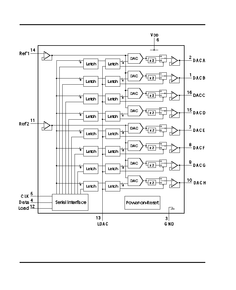
Pin Configuration
Ordering Information
Top View
16 pin N and DW packages
1
2
3
4
5
6
7
8
9
10
11
12
13
14
15
16
DACB
DACA
GND
Data
V
DD
DACE
CLK
DACF
DAC G
DACH
Ref2
LDAC
Load
Ref1
DACD
DACC
WM5628L, WM5628
Wolfson Microelectronics
2
WM5628L, WM5628
Block Diagram
Serial Interface
Power-on-Reset
DAC
DAC
DAC
DAC
DAC
DAC
DAC
DAC
Latch
Latch
Latch
Latch
Latch
Latch
Latch
Latch
Latch
Latch
Latch
Latch
Latch
Latch
Latch
Latch
x 2
x 2
x 2
x 2
x 2
x 2
x 2
x 2
9
9
9
9
9
9
9
9
8
8
8
8
8
8
8
8
Ref 1
Ref 2
CLK
Data
Load
LDAC
13
5
4
12
V
DD
DACA
2
1
DACB
DACC
16
15
DACD
DACE
7
8
DACF
9
DACG
DACH
10
11
14
3
GND
6
WM5628L, WM5628
Wolfson Microelectronics
3
PARAMETER SYMBOL TEST CONDITIONS MIN TYP MAX UNIT
Power Supply
Supply current
I
DD
Outputs unloaded,
4.0
mA
digital inputs = 0 V or V
DD
Static Accuracy
Resolution
8
Bits
Monotonicity
8
Bits
Differential Nonlinearity
DNL
V
REF
= 2 V, Range x 2. (note 3)
� 0.1
� 0.9
LSB
Integral Nonlinearity
INL
V
REF
= 2 V, Range x 2. (note 4)
� 1.0
LSB
Zero-code error
ZCE
V
REF
= 2 V, Range x 2. (note 5)
30
mV
Zero-code error
Input code = 00 Hex (note 6)
10
�
V/
O
C
temperature coefficient
Zero-code error supply
Input code = 00 Hex,
0.5
mV/V
rejection
V
DD
= 5 V � 5 % (note 7)
Full scale error
FSE
V
REF
= 2 V, Range x 2. (note 8)
� 60
mV
Full scale error
Input code = FF Hex (note 9)
� 25
�
V/
O
C
temperature coefficient
Full scale error supply
Input code = FF Hex,
0.5
mV/V
rejection
V
DD
= 5 V � 5 % (note 10)
Output sink current
I
O(SINK)
Each DAC output
20
�
A
Output source current
I
O(SOURCE)
2
mA
Absolute Maximum Ratings
(note 1)
Supply Voltage (VDD - VGND) . . . . . . . . . . . . +7V
Digital Inputs . . . . . . . . . . .GND - 0.3 V, V
DD
+ 0.3 V
Reference inputs . . . . . . . GND - 0.3 V, V
DD
+ 0.3 V
Operating temperature range, TA . . . . . . T
MIN
to T
MAX
WM5628_C_ . . . . . . . . . . . . . . 0oC to +70oC
WM5628_I_ . . . . . . . . . . . . . . . -40oC to +85oC
Storage Temperature . . . . . . . . . . -50oC to +150oC
Lead Temperature 1.6mm (1/16 inch)
from case for 10 secs . . . . . . . . . . . . . 260
O
C
Recommended Operating Conditions
SYMBOL MIN NOMINAL MAX UNIT
Supply voltage WM5628
V
DD
4.75
5.25
V
Supply Voltage WM5628L
V
DD
2.7
5.25
V
Reference input range
,
X1 gain
V
REF
3.3
V
DD
- 1.5
V
DAC output load resistance to GND
R
L
10
k
High level digital input voltage
V
IH
0.8 VDD
V
Low level digital input voltage
V
IL
0.8
V
Clock frequency
F
CLK
1
MHz
Electrical Characteristics: WM5628
V
DD
= 5 V, GND = 0 V, V
REF
= 2 V, R
L
= 10 k
, C
L
= 100 pF, T
A
= full range, unless otherwise stated.
Wolfson Microelectronics
4
WM5628L, WM5628
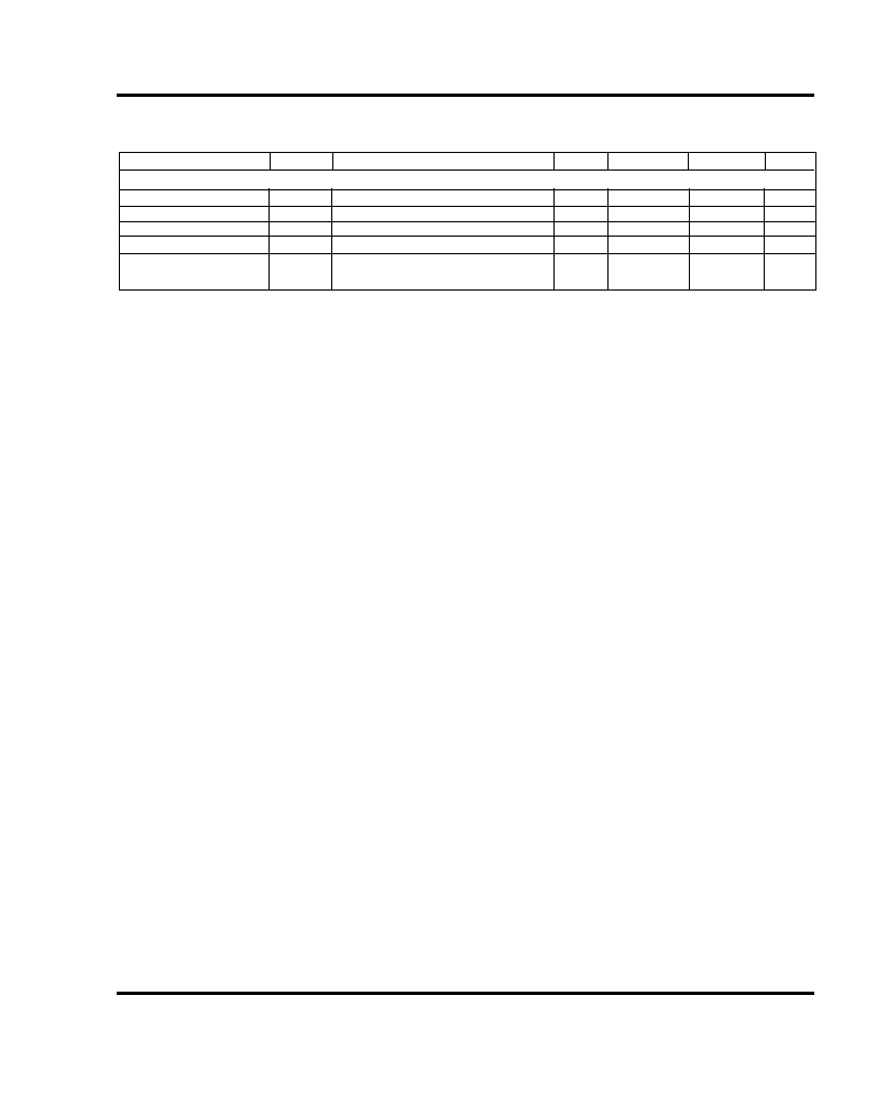
PARAMETER SYMBOL TEST CONDITIONS MIN TYP
MAX
UNIT
Power Supply
Supply current
I
DD
V
DD
= 3.3v
4
mA
Static Accuracy
Resolution
8
Bits
Monotonicity
8
Bits
Differential Nonlinearity DNL
V
REF
= 1.25 V, Range x 2. (note 3)
� 0.9
LSB
Integral Nonlinearity
INL
V
REF
= 1.25 V, Range x 2. (note 4)
� 1.0
LSB
Zero-code error
ZCE
V
REF
= 1.25 V, Range x 2. (note 5)
0
30
mV
Zero-code error
Input code = 00 Hex (note 6)
10
�
V/
O
C
temperature coefficient
Full scale error
FSE
V
REF
= 1.25 V, Range x 2. (note 8)
� 60
mV
Full scale error
Input code = FF Hex (note 9)
� 25
�
V/
O
C
temperature coefficient
Output sink current
I
O(SINK)
Each DAC output
20
�
A
Output source current
I
O(SOURCE)
1
mA
Power supply
I
REF
VDD = 3.3V, V
REF
= 1.5V
0.5
mV/V
sensitivity
PSRR
Electrical Characteristics: WM5628L
V
DD
= 3 .6V, GND = 0 V, V
REF
= 2 V x 1 gain, R
L
= 10 k
, C
L
= 100 pF, T
A
= full range, unless otherwise stated.
Electrical Characteristics: WM5628 & WM5628L
PARAMETER SYMBOL TEST CONDITIONS MIN TYP MAX UNIT
Digital Inputs
High level input current
I
IH
V
I
= V
DD
�10
�
A
Low level input current
I
IL
V
I
= 0V
�10
�
A
Input capacitance
C
I
15
pF
Timing Parameters
Data input setup time
t
SD
50
ns
Data input hold time
t
HD
50
ns
CLK
to Load
t
HL
50
ns
Load
to CLK
t
SL
50
ns
Load duration
t
WL
250
ns
LDAC duration
t
WD
250
ns
Load
to LDAC
t
LD
0
ns
Reference Inputs
Reference input
V
REF
A, B, C, D, inputs
GND
V
DD
-1.5
V
voltage
Reference input
A, B, C, D, inputs
15
pF
capacitance
Reference
A, B, C, D inputs (note 11)
-60
dB
feedthrough
Channel to channel
A, B, C, D inputs (note 12)
-60
dB
isolation
V
DD
= 2.7 to 5.5V, GND = 0 V, V
REF
= 2 V x 1 gain, R
L
= 10 k
, C
L
= 100 pF, T
A
= full range, unless otherwise stated.
WM5628L, WM5628
Wolfson Microelectronics
5
PARAMETER SYMBOL TEST CONDITIONS MIN TYP MAX UNIT
Dynamic Performance
Output settling time
To 1/2LSB, VDD=3V & 5V (note 13)
10
�
s
Output slew rate
1
V/
�
s
Input bandwidth
(note 14)
100
kHz
Large Signal Bandwidth
Measured at -3dB point
100
kHz
Digital Crosstalk
Clk = 1MHz sq wave measured at
-50
dB
DACA - DACD
Electrical Characteristics: WM5628 & WM5628L
(continued)
V
DD
= 3 .6V, GND = 0 V, V
REF
= 2 V x 1 gain, R
L
= 10 k
, C
L
= 100 pF, T
A
= full range, unless otherwise stated.
Notes:
1.
Absolute Maximum Ratings are stress ratings only.
Permanent damage to the device may be caused by
continuously operating at or beyond these limits.
Device functional operating range limits are given
under Recommended Operating Conditions.
Guaranteed performance specifications are given
under Electrical Characteristics at the test conditions
specified.
2.
Total Unadjusted Error is the sum of integral linearity
error, zero code error and full scale error over the input
code range.
3.
Differential Nonlinearity (DNL) is the difference
between the measured and ideal 1 LSB amplitude
change of any two adjacent codes. A guarantee of
monotonicity means the output voltage changes in the
same direction (or remains constant) as a change in
the digital input code.
4.
Integral Nonlinearity (INL) is the maximum deviation of
the output from the line between zero and full scale
(excluding the effects of zero code and full-scale
errors).
5.
Zero code error is the deviation from zero voltage
output when the digital input code is zero.
6.
Zero code error temperature coefficient is given by:
ZCETC = (ZCE(T
max
- ZCE(T
min
)) /V
REF
x 10
6
/ (T
max
- T
min
)
7.
Zero-code Error Rejection Ratio (ZCE-RR) is
measured by varying the V
DD
voltage, from 4.5 to 5.5
V d.c., and measuring the proportion of this signal
imposed on the zero-code output voltage.
8.
Full-scale error is the deviation from the ideal full-scale
output (V
REF
- 1LSB) with an output load of 10k
9.
Full-Scale Temperature Co-efficient is given by:
FSETC = (FSE(T
max
) - FSE(T
min
)) / V
REF
x 10
6
/ T
max
- T
min
)
10. Full Scale Error Rejection Ratio (FSE-RR) is
measured by varying the V
DD
voltage from 4.5 to
5.5 V d.c. and measuring the proportion of this signal
imposed on the full-scale output voltage
11 Reference feedthrough is measured at a DAC output
with an input code = 00 Hex with a V
REF
input = 1 V
dc
+ 1 V
PP
at 10kHz
12. Channel to channel isolation is measured at a DAC
output with an input code of one DAC to FF Hex and
the code oa all other DACs to oo Hex with a V
REF
in-
put = 1 V
dc
+ 1 V
pp
at 10kHz
13 Setting time is the time for the output signal to remain
within �0.5 LSB of the final measurement value for a
digital input code change of 00 Hex to FF Hex. For
WM 5628: V
DD
= 5V, V
REF
= 2V and range = x 2. For
WM5628L: V
DD
= 3, V
REF
= 1.25V and range = x 2.
14 Reference bandwidth is the -3dB bandwidth with an
input at V
REF
= 1.25 V
dc
=+ 2 V
pp
with a digital input
code of full-scale.
Wolfson Microelectronics
6
WM5628L, WM5628
Parameter Measurement Information
DACA
DACB
DACC
.
.
DACH
10K
CL - 100pF
Slewing Settling Time and Linearity Measurements
Typical Performance Characteristics
Typical DNL, INL and TUE * at V
DD
= 5 V
* see note 2
Diffe re ntia l Nonlinea rity
V
DD
= 5 V, Vref = 2.5 V, Rang e x 1, T
A
= 25
o
C
-0.2
-0.1
0
0.1
0.2
0
32
64
96
128
160
192
224
256
Inpu t Code
Error (lsb)
Integral Nonlinearity
V
DD
= 5 V, Vref =2.5 V, Ra ng e x 1, T
A
= 25
o
C
-0.2
0
0.2
0.4
0
32
64
96
128
160
192
224
256
Inp ut Code
Error (lsb)
Total Unadjusted Error
V
DD
= 5 V, Vref = 2.5 V, Rang e x 1, T
A
= 25
o
C
-0.5
-0.25
0
0.25
0.5
0
32
64
96
128 160
192 224 256
Input C ode
Error (lsb)
Diffe re ntia l Nonline a rity
V
DD
= 5 V, Vref = 1.25 V, Ra ng e x 2, T
A
= 25
o
C
-0.2
-0.1
0
0.1
0.2
0
32
64
96
128
160
192
224
256
Inpu t Code
Error (l
s
WM5628L, WM5628
Wolfson Microelectronics
7
Typical Performance Characteristics
(continued)
Inte gra l Nonline a rity
V
DD
= 5 V, Vref = 1.25 V, Ra nge x 2, T
A
= 25
o
C
-0.2
0
0.2
0.4
0
32
64
96
128
160
192
224
256
Inp ut C od e
Error (l
s
Tota l Una d justed Error
V
DD
= 5 V, Vref = 1.25 V, Ra nge x 2, T
A
= 25
o
C
-0.5
-0.25
0
0.25
0.5
0
32
64
96
128
160
192
224
256
Inpu t Code
Error (l
s
Diffe re ntia l Nonlinea rity
VDD = 3 V, V re f = 1.25 V , Ra n g e x 2, TA = 25
o
C
-0.2
-0.1
0
0.1
0.2
0
32
64
96
128
160
192
224
256
Inpu t Code
Error (lsb)
Integral Nonlinearity
V
DD
= 3 V, Vref = 1.25 V, Rang e x 2, T
A
= 25
o
C
-0.5
-0.25
0
0.25
0.5
0
32
64
96
128
160
192
224
256
Inp ut Code
Error (lsb)
Total Unadjusted Error
V
DD
= 3 V, Vref = 1.25 V, Rang e x 2, T
A
= 25
o
C
-0.5
-0.25
0
0.25
0.5
0
32
64
96
128
160
192
224
256
Inp ut C od e
Error (l
s
Typical DNL, INL and TUE at VDD = 3 V
Typical DNL, INL and TUE * at V
DD
= 5 V
(continued)
Output Source Current
vs Output Voltage
0
1
2
3
4
5
6
7
8
0
1
2
3
4
5
V
out
(V)
I
out
(mA
)
V
DD
= 5 V
T
A
= 25
O
C
V
ref
= 2 V
Range = x 2
Input c ode = 255
Supply Current vs
Temperature
1.4
1.6
1.8
2
2.2
2.4
-50
-25
0
25
50
75
100
Temperature ('C)
I
DD
(mA
)
Ran ge = x 2
Input C ode = 255
V
DD
= 5V
V
re f
= 2V
V
DD
+ 3V
V
re f
= 1.25V
o
C
Wolfson Microelectronics
8
WM5628L, WM5628
Typical Performance Characteristics
(continued)
Large Signal Frequency
Response
-20
-18
-16
-14
-12
-10
-8
-6
-4
-2
0
2
1
10
100
1000
Frequency (kHz)
Relative Gain (dB
)
V
DD
= 5 V
T
A
= 25
O
C
V
ref
= 1.25 V
d c
+ 2 V
pp
Input Code = 255
Small Signal Frequency
Response
-60
-50
-40
-30
-20
-10
0
10
1
10
100
1000
10000
Frequency (kHz)
Relative Gain (dB
)
V
DD
= 5 V
T
A
= 25
O
C
Vref = 2 V
d c
+ 0.5 V
pp
Input c od e = 255
Positive Rise and Settling Time VDD = 5 V
Positive Rise and Settling Time VDD = 3 V
Fall time = 4.85
�
s, Negative slew rate = 0.41
�
s
Settling time = 8.0
�
s
Fall time = 5.9
�
s, Negative slew rate = 0.54
�
s
Settling time = 8.5
�
s
Rise time = 2.5
�
s, Positive slew rate = 0.80
�
s
Settling time = 4.5
�
s
Rise time = 3.75
�
s, Positive slew rate = 0.54
�
s
Settling time = 5.9
�
s
500 mV/Vert. div
2
�
s/Hor. div
500 mV/Vert. div
2
�
s/Hor. div
1 V/Vert. div
2
�
s/Hor. div
VDD = 3 V
T
A
= 25
O
C
code 00 to FF Hex
Range = x 2
Vref = 1.25 V
1 V/Vert. div
5
�
s/Hor. div
Negative Fall and Settling Time VDD = 3 V
Negative Fall and Settling Time VDD = 5 V
V
DD
= 3 V
T
A
= 25
O
C
code FF to 00 Hex
Range = x 2
Vref = 1.25 V
V
DD
= 5 V
T
A
= 25
O
C
code 00 to FF Hex
Range = x 2
Vref = 2 V
VDD = 5 V
TA = 25
O
C
code FF to 00 Hex
Range = x 2
Vref = 2 V

WM5628L, WM5628
Wolfson Microelectronics
9
Equivalent Input and Output Circuits
Timing Waveforms
CLK
50 %
t
SD
t
HD
Data
Data Input Timing
50 %
CLK
t
HL
t
WL
t
SL
t
LD
t
WD
Load and LDAC Timing
Load
LDAC
Wolfson Microelectronics
10
WM5628L, WM5628
A1
A2
A0
RNG
D7
D6
D5
D4
D3
D2
D1
D0
1
2
3
4
5
6
7
8
9
10
11
12
CLK
Data
Load
LDAC
A1
A2
A0
RNG
D7
D6
D5
D4
D3
D2
D1
D0
1
2
3
4
5
6
7
8
9
10
11
12
CLK
Data
Load
LDAC
Figure 4. LDAC controlled update using 8-bit serial word.
Figure 3. Load controlled update (LDAC = 0) using 8-bit serial word.
Figure 1. Load controlled update (LDAC = 0)
Timing Diagrams
Figure 2. LDAC controlled update
CLK
Data
Load
LDAC
A2
A1
A0
RNG
D7
D6
D5
D4
D3
D2
D1
D0
1
2
3
4
5
6
7
8
9
10
11
12
CLK
Data
Load
LDAC
A2
A1
A0
RNG
D7
D6
D5
D4
D3
D2
D1
D0
1
2
3
4
5
6
7
8
9
10
11
12

WM5628L, WM5628
Wolfson Microelectronics
11
Pin Descriptions
Pin
Name
Type
Function
1
DACB
Analogue output
DAC B output
2
DACA
Analogue input
DAC A output
3
GND
Supply
Ground return
4
Data
Digital input
Serial data input
5
CLK
Digital input
Serial interface clock, negative edge sensitive
6
V
DD
Supply
Positive supply voltage
7
DACE
Analogue output
DAC E output
8
DACF
Analogue output
DAC F output
9
DACG
Analogue output
DAC G output
10
DACH
Analogue output
DAC H output
11
Ref2
Analogue input
Reference to DACE, DACF, DACG and DACH
12
Load
Digital input
Serial input load
13
LDAC
Digital input
DAC update latch control
14
Ref1
Analogue input
Reference to DACA, DACB, DACC and DACD
15
DACD
Analogue output
DAC D output
16
DACC
Analogue output
DAC C output
Functional Description
DAC operation
Each of WM5628/L 's eight digital to analogue converters
(DACs) are implemented using a single resistor string with
256 taps corresponding to each of the input 8-bit codes.
One end of a resistor string is connected to the GND pin
and the other end is driven from the output of a reference
input buffer. The use of a resistor string guarantees
monotonicity of the DAC's output voltage. Linearity depends
upon the matching of the resistor string's individual elements
and the performance of the output buffer. Two high input
impedance voltage reference buffers are provided, each
driving four DACs,
Each DAC has a voltage output amplifier which is
programmable for gains of x1 or x 2 through the serial
interface. The DAC output amplifiers feature rail to rail
output stages, allowing outputs over the full supply voltage
range to be achieved with a x 2 gain setting and a V
DD
/2
reference voltage input. Used in this way a slight
degradation in linearity will occur as the output voltage
approaches V
DD
.
A power-on-reset activates at power up resetting the DACs
inputs to code 0. Each output voltage is given by:
V
out
= V
ref
x CODE/256 x (RNG+1 )
Where:
RNG controls the output gains of x 1 and x 2
CODE is the range 0 to 255
Data Interface
WM5628/L's eight double buffered DAC inputs allow
several ways of controlling the update of each DAC's
output.
Serial data is input, MSB first, into the DATA input pin Serial
Input DAC Address and Output Tables using CLK, LOAD
and LDAC control inputs and comprises 3 DAC address
bits, an output range (RNG) bit and 8 DAC input bits.
With the LOAD pin high data is clocked into the DATA pin
on each falling edge of CLK. Any number of data bits may
be clocked in, only the last 12 bits are used. When all data
bits have been clocked in, a falling edge at the LOAD pin
latches the data and RNG bits into the correct 9 bit input
latch using the 3 bit DAC address.
If the LDAC input pin is low, the second latch at the DAC
input is transparent, and the DAC input and RNG bit will be
updated on the falling edge of LOAD simultaneously with
the input latch, as shown in figure 1. If the LDAC input is high
during serial data input, as shown in figure 2, the falling edge
of the LOAD input stores the data in the addressed input
latch. The falling edge of LDAC updates the second latches
from the input latches and hence the DAC outputs.
Wolfson Microelectronics
12
WM5628L, WM5628
Serial Input DAC Address and Output Tables
Using these inputs individual DACs can be updated using
one 12 bit serial input word and the LOAD pin. Using both
LOAD and LDAC, all or selected DACs can be updated
after an appropriate number of data words have been
inputted. Figures 3 &4 illustrate operation with the 8 clock
pulses available from some microprocessors. If the data
input is interrupted in this way the clock input must be held
low during the break in clock pulses.
The RNG bit controls the DAC output range. When RNG = 0
the output is between Vref(A,B,C,D) and GND and when
RNG = 1 the range is between 2 x Vref (A,B,C,D) and GND.
Functional Description
(continued)
A2 A1
A0 DAC Updated
0
0
0
DACA
0
0
1
DACB
0
1
0
DACC
0
1
1
DACD
1
0
0
DACE
1
0
1
DACF
1
1
0
DACG
1
1
1
DACH
D7 D6 D5 D4 D3 D2 D1 D0
Output Voltage
0
0
0
0
0
0
0
0
GND
0
0
0
0
0
0
0
1
(1/256) x Ref (1 + RNG)
0
1
1
1
1
1
1
1
(127/256) x Ref (1 + RNG)
1
0
0
0
0
0
0
0
(128/256) x Ref (1 + RNG)
1
1
1
1
1
1
1
1
(255/256) x Ref (1 + RNG)

WM5628L, WM5628
Wolfson Microelectronics
13
Functional Description
(Continued)
Linearity, offset, and gain error using
single end supplies
When an amplifier is operated from a single supply, the
voltage offset can still be either positive or negative. With a
positive offset, the output voltage changes on the first code
change. With a negative offset the output voltage may not
change with the first code depending on the magnitude of
the offset voltage.
The output amplifier, with a negative voltage offset, attempts
to drive the output to a negative voltage. However, because
the most negative supply rail is GND, the output cannot drive
to a negative voltage.
So when the output offset voltage is negative, the output
voltage remains at ZERO volts until the input code value
produces a sufficient output voltage to overcome the
inherent negative offset voltage, resulting in the transfer
function shown below
Effect of negative offset (single supply)
This negative offset error, not the linearity error, produces
this breakpoint. The transfer function would have followed
the dotted line if the output buffer could drive to a negative
voltage.
For a DAC, linearity is measured between ZERO input code
( all inputs 0 ) and full scale code ( all inputs 1 ) after offset
and full scale are adjusted out or accounted for in some way.
However, single supply operation does not allow for
adjustment when the offset is negative due to the break-
point in the transfer function. So the linearity in the unipolar
mode is measured between full scale code and the lowest
code which produces a positive output voltage. The code is
calculated from the maximum specification for the negative
offset.
Wolfson Microelectronics
14
WM5628L, WM5628
Package Descriptions
Notes:
A. Dimensions are in inches
B. Falls within JEDEC MS-001( 20 pin package is shorter than MS-001)
C. N is the maximum number of terminals
D. All end pins are partial width pins as shown, except the 14 pin package which is full width.
Dimension 'A' Variations
Dual-In-Line Package
N or P
Rev. 1 November 96
N
Min
Max
8
0.355
0.400
14
0.735
0.775
16
0.735
0.775
20
0.940
0.975
0.210 Max.
0.070 Max.
0.045
0.030
0.022
0.014
0.015
Min.
0.150
0.115
0.005
Min.
Pin spacing
0.100 B.S.C.
1
N
Seating
plane
0.280
0.240
0.325
0.290
0.014
0.008
105
90
O
O
N/2
A
WM5628L, WM5628
Wolfson Microelectronics
15
Package Description
Wide body Plastic Small-Outline Package
1,27 B.S.C.
0,51
0,33
0,25
M
9
16
7,60
7,40
10,65
10,00
A
1
8
2,65
2,35
0,30
0,10
1,27
0,40
Gauge Plane
0
o
- 8
o
0,10
Notes:
A. Dimensions in millimeters.
B. Complies with Jedec standard MS-013.
C. This drawing is subject to change without notice.
D. Body dimensions do not include mold flash or protrusion.
E. Dimension A, mould flash or protrusion shall not exceed 0.15mm. Body width, interlead flash or protrusions shall not
exceed 0.25mm.
DW - 16 pin shown
DIM
A MIN
A MAX
PINS**
16
10,50
20
13,00
10,10
12,60
24
15,60
15,20
18,10
28
17,70
0.75 x 45
0
0.25 x 45
0
Rev. 1 November 96
0,33
0,23