Document Outline
- WM8521
- Stereo DAC With Integrated Output Stage for 2Vrms LINE OUT
- DESCRIPTION
- FEATURES
- APPLICATIONS
- BLOCK DIAGRAM
- TABLE OF CONTENTS
- PIN CONFIGURATION
- ORDERING INFORMATION
- PIN DESCRIPTION
- ABSOLUTE MAXIMUM RATINGS
- DC ELECTRICAL CHARACTERISTICS
- ELECTRICAL CHARACTERISTICS
- MASTER CLOCK TIMING
- DEVICE DESCRIPTION
- GENERAL INTRODUCTION
- DAC CIRCUIT DESCRIPTION
- CLOCKING SCHEMES
- DIGITAL AUDIO INTERFACE
- AUDIO DATA SAMPLING RATES
- HARDWARE CONTROL MODES
- DIGITAL FILTER CHARACTERISTICS
- DAC FILTER RESPONSES
- DIGITAL DE-EMPHASIS CHARACTERISTICS
- APPLICATIONS INFORMATION
- RECOMMENDED EXTERNAL COMPONENTS
- RECOMMENDED EXTERNAL COMPONENTS VALUES
- RECOMMENDED ANALOGUE LOW PASS FILTER
- PCB LAYOUT RECOMMENDATIONS
- PACKAGE DRAWING
- IMPORTANT NOTICE
- ADDRESS:

w
WM8521
Stereo DAC With Integrated Output Stage
for 2Vrms LINE OUT
WOLFSON MICROELECTRONICS plc
www.wolfsonmicro.com
Product Preview, December 2004, Rev 1.3
Copyright
2004 Wolfson Microelectronics plc
.
DESCRIPTION
The WM8521 is a 96kHz stereo DAC with an integrated output
op-amp stage, designed to generate a 2.0Vrms output signal
directly, so reducing external component requirements in digital
audio applications.
WM8521 comes into two variants WM8521HC and WM8521H9
which offers different line drive output capabilities. WM8521HC
outputs 2Vrms at 12V supply, while WM8521H9 outputs
2.0Vrms at 9V supply. WM8521HC/H9 are designed for cost
sensitive consumer digital audio applications requiring 2Vrms
line output.
A 24-bit multi-bit sigma delta DAC is used with oversampling
digital interpolation filters. Digital audio input word lengths from
16-32 bits and sampling rates from 8kHz to 96kHz are
supported.
The audio interface supports I
2
S, Right Justified and DSP digital
audio formats.
The devices are controlled via a hardware interface which
provides access to features including de-emphasis, mute and
data formats. These devices are pin equivalent and are
available in a 14-pin SOIC package.
FEATURES
∑
Audio
Performance
- DAC SNR 98dB (`A' weighted @ 48kHz)
- THD -81dB (`A' weighted @ 48kHz)
∑
DAC Sampling Frequency: 8kHz ≠ 96kHz
∑
Pin Selectable Audio Data Interface Format
- I
2
S, 16-bit Right Justified or 16bit DSP
∑
2.0 Vrms output at 12V or 9V supply
∑
8.2V to 13.2V Analogue, 2.7V to 3.6 Digital Supply
∑
14-pin SOIC Package
APPLICATIONS
∑
Consumer digital audio applications requiring 2 Vrms output
- DVD Players
- Digital TV
- Digital Set Top Boxes
- A/V Receivers
BLOCK DIAGRAM

WM8521
Product Preview
w
PP Rev 1.3 December 2004
2
TABLE OF CONTENTS
DESCRIPTION .......................................................................................................1
FEATURES.............................................................................................................1
APPLICATIONS .....................................................................................................1
BLOCK DIAGRAM .................................................................................................1
PIN CONFIGURATION...........................................................................................3
ORDERING INFORMATION ..................................................................................3
ABSOLUTE MAXIMUM RATINGS .........................................................................5
DC ELECTRICAL CHARACTERISTICS ................................................................6
ELECTRICAL CHARACTERISTICS ......................................................................6
TERMINOLOGY............................................................................................................. 7
MASTER CLOCK TIMING.............................................................................................. 8
DIGITAL AUDIO INTERFACE........................................................................................ 8
DEVICE DESCRIPTION .........................................................................................9
GENERAL INTRODUCTION.......................................................................................... 9
DAC CIRCUIT DESCRIPTION....................................................................................... 9
CLOCKING SCHEMES ................................................................................................ 10
DIGITAL AUDIO INTERFACE...................................................................................... 10
AUDIO DATA SAMPLING RATES ............................................................................... 12
HARDWARE CONTROL MODES................................................................................ 13
DIGITAL FILTER CHARACTERISTICS ....................................................................... 15
DAC FILTER RESPONSES ......................................................................................... 15
DIGITAL DE-EMPHASIS CHARACTERISTICS ........................................................... 16
APPLICATIONS INFORMATION .........................................................................17
RECOMMENDED EXTERNAL COMPONENTS........................................................... 17
RECOMMENDED EXTERNAL COMPONENTS VALUES............................................ 17
RECOMMENDED ANALOGUE LOW PASS FILTER ................................................... 18
PCB LAYOUT RECOMMENDATIONS......................................................................... 18
PACKAGE DRAWING..........................................................................................19
IMPORTANT NOTICE ..........................................................................................20
ADDRESS:................................................................................................................... 20
Product Preview
WM8521
w
PP Rev 1.3 December 2004
3
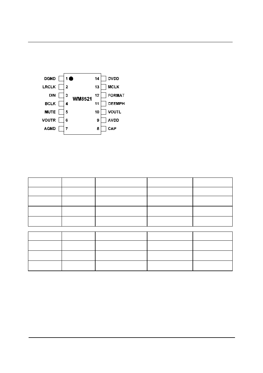
PIN CONFIGURATION
ORDERING INFORMATION
DEVICE
TEMPERATURE
RANGE
PACKAGE
MOISTURE SENSITIVITY
LEVEL
PEAK SOLDERING
TEMPERATURE
WM8521HCED/V
-25 to +85
o
C 14-pin
SOIC
MSL1
240
o
C
WM8521HCED/RV
-25 to +85
o
C
14-pin SOIC
(tape and reel)
MSL1
240
o
C
WM8521HCGED/V
-25 to +85
o
C
14-pin SOIC
(lead free)
MSL1
260
o
C
WM8521HCGED/RV
-25 to +85
o
C
14-pin SOIC
(lead free, tape and reel)
MSL1
260
o
C
WM8521H9ED/V
-25 to +85
o
C 14-pin
SOIC
MSL1
240
o
C
WM8521H9ED/RV
-25 to +85
o
C
14-pin SOIC
(tape and reel)
MSL1
240
o
C
WM8521H9GED/V
-25 to +85
o
C
14-pin SOIC
(lead free)
MSL1
260
o
C
WM8521H9GED/RV
-25 to +85
o
C
14-pin SOIC
(lead free, tape and reel)
MSL1
260
o
C
Note:
1.
Reel quantity = 3,000
2.
WM8521H9: 2Vrms output at 9V supply
3.
WM8521HC: 2Vrms output at 12V supply
WM8521
Product Preview
w
PP Rev 1.3 December 2004
4
PIN DESCRIPTION
PIN NAME
TYPE
DESCRIPTION
1
DGND Supply
Digital
Negative
supply
2
LRCLK
Digital input
Sample rate clock input
3
DIN
Digital input
Serial audio data input
4
BCLK
Digital input
Bit clock input
5
MUTE
Digital input
Soft mute control, Internal pull down
High Impedance = Automute
High = Mute ON
Low = Mute OFF
6
VOUTR
Analogue output
Right channel DAC output
7
AGND Supply
Analogue
Negative
supply
8
CAP
Analogue output
Analogue internal reference
9
AVDD
Supply
Analogue Positive supply
10
VOUTL
Analogue output
Left channel DAC output
11
DEEMPH
Digital input
De-emphasis select, Internal pull down
High = de-emphasis ON
Low = de-emphasis OFF
12
FORMAT
Digital input
Data input format select, Internal pull up
Low = 16-bit right justified or 16bit DSP `late'
High = 16-32-bit I
2
S or 16bit DSP `early'
13
MCLK
Digital input
Master clock input
14
DVDD
Supply
Digital Positive supply
Note:
1.
Digital input pins have Schmitt trigger input buffers.

Product Preview
WM8521
w
PP Rev 1.3 December 2004
5
ABSOLUTE MAXIMUM RATINGS
Absolute Maximum Ratings are stress ratings only. Permanent damage to the device may be caused by continuously operating at
or beyond these limits. Device functional operating limits and guaranteed performance specifications are given under Electrical
Characteristics at the test conditions specified.
ESD Sensitive Device. This device is manufactured on a CMOS process. It is therefore generically susceptible
to damage from excessive static voltages. Proper ESD precautions must be taken during handling and storage
of this device.
Wolfson tests its package types according to IPC/JEDEC J-STD-020B for Moisture Sensitivity to determine acceptable storage
conditions prior to surface mount assembly. These levels are:
MSL1 = unlimited floor life at <30
∞
C / 85% Relative Humidity. Not normally stored in moisture barrier bag.
MSL2 = out of bag storage for 1 year at <30
∞
C / 60% Relative Humidity. Supplied in moisture barrier bag.
MSL3 = out of bag storage for 168 hours at <30
∞
C / 60% Relative Humidity. Supplied in moisture barrier bag.
The Moisture Sensitivity Level for each package type is specified in Ordering Information.
CONDITION
MIN MAX
Analogue Supply Voltage (AVDD)
-0.3V +15V
Digital Supply voltage (DVDD)
-0.3V +4.2V
Voltage range digital inputs
DGND -0.3V
DVDD +0.3V
Master Clock Frequency
50MHz
Operating temperature range, T
A
-25
∞
C +85
∞
C
Storage temperature prior to soldering
30
∞
C max / 85% RH max
Storage temperature after soldering
-65
∞
C +150
∞
C