Document Outline
- WM8737L
- Stereo ADC with Microphone Preamplifier
- DESCRIPTION
- FEATURES
- APPLICATIONS
- BLOCK DIAGRAM
- TABLE OF CONTENTS
- PIN CONFIGURATION
- ORDERING INFORMATION
- PIN DESCRIPTION
- ABSOLUTE MAXIMUM RATINGS
- RECOMMENDED OPERATING CONDITIONS
- ELECTRICAL CHARACTERISTICS
- POWER CONSUMPTION
- SIGNAL TIMING REQUIREMENTS
- DEVICE DESCRIPTION
- INTRODUCTION
- INPUT SIGNAL PATH
- ANALOGUE TO DIGITAL CONVERTER (ADC)
- 3D STEREO ENHANCEMENT
- AUTOMATIC LEVEL CONTROL (ALC)
- DIGITAL AUDIO INTERFACE
- MASTER CLOCK AND AUDIO SAMPLE RATES
- CONTROL INTERFACE
- POWER SUPPLIES
- POWER MANAGEMENT
- REGISTER MAP
- DIGITAL FILTER CHARACTERISTICS
- APPLICATIONS INFORMATION
- LINE INPUT CONFIGURATION
- MICROPHONE INPUT CONFIGURATION
- RECOMMENDED EXTERNAL COMPONENTS
- PACKAGE DIMENSIONS
- IMPORTANT NOTICE

w
WM8737L
Stereo ADC with Microphone Preamplifier
WOLFSON MICROELECTRONICS plc
www.wolfsonmicro.com
Advanced Information, May 2004, Rev 3.0
Copyright
2004 Wolfson Microelectronics plc
DESCRIPTION
The WM8737L is a low power stereo audio ADC designed
specifically for portable applications such as minidisc and
memory audio / voice recorders.
The device offers three sets of stereo inputs, which can be
configured for line-level signals, for internal or table-top
microphones, or for DC measurement (battery monitor). A
programmable gain amplifier can be used for automatic
level control (ALC) with user programmable hold, attack and
decay times. The device also has a selectable high pass
filter to remove residual DC offsets.
If the signal source is mono, the WM8737L can run in mono
mode, saving power. It can also mix two channels to mono,
either in the analogue or the digital domain.
Master or slave mode clocking schemes are offered. Stereo
24-bit multi-bit sigma-delta ADCs are used with digital audio
output word lengths from 16-32 bits, and sampling rates
from 8kHz to 96kHz supported.
The device is controlled via a 2 or 3 wire serial interface.
The interface provides access to all features including gain
controls, analogue or digital mono mixing, and power
management facilities. The device is supplied in a leadless
5x5mm QFN package.
FEATURES
�
SNR 97dB (`A' weighted @ 3.3V, 48kHz, normal power
mode)
�
THD �85dB (at �1dB, 3.3V, normal power mode)
�
Complete Stereo / Mono Microphone Interface
- Programmable microphone preamp
- Automatic
Level
Control
- Low-noise microphone bias voltage
�
Configurable Power / Performance
�
Low
Power
Mode
- 8.5mW at AVDD = 1.8V (stereo, mic preamps off)
- 20mW at AVDD = 3.3V (stereo, mic preamps off)
�
Low Supply Voltages
- Analogue 1.8V to 3.6V
- Digital core: 1.42V to 3.6V
- Digital I/O: 1.8V to 3.6V
�
256fs / 384fs or USB master clock rates: 12MHz, 24MHz
�
Audio sample rates: 8, 11.025, 12, 16, 22.05, 24, 32, 44.1,
48, 88.2, 96kHz generated internally from master clock
�
32-pin QFN package, 5 x 5 x 0.9mm
APPLICATIONS
�
Memory Audio / Voice Recorders
�
Minidisc
Recorders
�
Portable Digital Music Systems
BLOCK DIAGRAM

WM8737L
Preliminary Technical Data
w
AI Rev 3.0 May 2004
2
TABLE OF CONTENTS
DESCRIPTION .......................................................................................................1
FEATURES.............................................................................................................1
APPLICATIONS .....................................................................................................1
BLOCK DIAGRAM .................................................................................................1
TABLE OF CONTENTS .........................................................................................2
PIN CONFIGURATION...........................................................................................3
ORDERING INFORMATION ..................................................................................3
PIN DESCRIPTION ................................................................................................4
ABSOLUTE MAXIMUM RATINGS .........................................................................5
RECOMMENDED OPERATING CONDITIONS .....................................................5
ELECTRICAL CHARACTERISTICS ......................................................................6
TERMINOLOGY............................................................................................................. 8
NOTES........................................................................................................................... 8
POWER CONSUMPTION ......................................................................................9
SIGNAL TIMING REQUIREMENTS .....................................................................11
DEVICE DESCRIPTION .......................................................................................14
INTRODUCTION.......................................................................................................... 14
INPUT SIGNAL PATH.................................................................................................. 14
ANALOGUE TO DIGITAL CONVERTER (ADC) .......................................................... 19
3D STEREO ENHANCEMENT..................................................................................... 20
AUTOMATIC LEVEL CONTROL (ALC) ....................................................................... 21
DIGITAL AUDIO INTERFACE...................................................................................... 24
MASTER CLOCK AND AUDIO SAMPLE RATES ........................................................ 28
CONTROL INTERFACE .............................................................................................. 30
POWER SUPPLIES ..................................................................................................... 31
POWER MANAGEMENT ............................................................................................. 31
REGISTER MAP...................................................................................................32
DIGITAL FILTER CHARACTERISTICS ...............................................................33
TERMINOLOGY........................................................................................................... 33
APPLICATIONS INFORMATION .........................................................................35
LINE INPUT CONFIGURATION................................................................................... 35
MICROPHONE INPUT CONFIGURATION .................................................................. 35
RECOMMENDED EXTERNAL COMPONENTS ..................................................36
PACKAGE DIMENSIONS ....................................................................................37
IMPORTANT NOTICE ..........................................................................................38
ADDRESS:................................................................................................................... 38

Preliminary Technical Data
WM8737L
w
AI Rev 3.0 May 2004
3
PIN CONFIGURATION
ORDERING INFORMATION
ORDER CODE
TEMPERATURE RANGE
PACKAGE
MOISTURE SENSITIVITY
LEVEL
PEAK SOLDERING
TEMPERATURE
WM8737LGEFL -25
�
C to +85
�
C
32-pin QFN (5x5x0.9mm)
lead free
MSL1 260�C
WM8737LGEFL/R -25
�
C to +85
�
C
32-pin QFN (5x5x0.9mm)
lead free, tape
and reel
MSL1 260�C
Note:
Reel Quantity = 3,500

WM8737L
Preliminary Technical Data
w
AI Rev 3.0 May 2004
4
PIN DESCRIPTION
PIN NO
NAME
TYPE
DESCRIPTION
1 NC
No Connect
No Internal Connection
2 SCLK
Digital Input
Control Interface Clock Input
3 DBVDD
Supply
Digital Buffer (I/O) Supply
4 DCVDD
Supply Digital
Core
Supply
5 DGND
Supply
Digital Ground (return path for both DCVDD and DBVDD)
6 NC
No Connect
No Internal Connection
7 MCLK
Digital Input
Master Clock
8 BCLK
Digital Input / Output
Audio Interface Bit Clock
9 ADCDAT Digital Output
ADC Digital Audio Data
10 ADCLRC Digital Input / Output
Audio Interface Left / Right Clock
11 MODE
Digital Input
Control Interface Selection
12 AGND
Supply
Analogue Ground (return path for both AVDD and MVDD)
13 MICBIAS Analogue Output
Microphone Bias
14
MVDD
Supply
Microphone Bias and Microphone Pre-amplifier Positive Supply
15 AVDD
Supply
Analogue Positive Supply
16 RACIN Analogue Input
Right Channel DC Blocking Capacitor
17 RACOUT Analogue Output
Right Channel DC Blocking Capacitor
18 RINPUT3 Analogue Input
Right Channel Input 3
19 RINPUT2 Analogue Input
Right Channel Input 2
20 RINPUT1 Analogue Input
Right Channel Input 1
21 LINPUT1 Analogue Input
Left Channel Input 1
22 LINPUT2 Analogue Input
Left Channel Input 2
23 LINPUT3 Analogue Input
Left Channel Input 3
24 LACOUT Analogue Output
Left Channel DC Blocking Capacitor
25 LACIN Analogue Input
Left Channel DC Blocking Capacitor
26 VMID Analogue Output
Midrail Voltage Decoupling Capacitor
27 VREF Analogue Output
Reference Voltage Decoupling Capacitor
28 VREFP Analogue Output
Positive Reference Decoupling Connection
29 VREFN Analogue Output
Negative Reference Decoupling Connection
30 AGND
Supply
Analogue Ground (return path for both AVDD and MVDD)
31 CSB
Digital Input
Chip Select / Device Address Selection
32 SDIN Digital Input / Output
Control Interface Data Port

Preliminary Technical Data
WM8737L
w
AI Rev 3.0 May 2004
5
ABSOLUTE MAXIMUM RATINGS
Absolute Maximum Ratings are stress ratings only. Permanent damage to the device may be caused by continuously
operating at or beyond these limits. Device functional operating limits and guaranteed performance specifications are given
under Electrical Characteristics at the test conditions specified.
ESD Sensitive Device. This device is manufactured on a CMOS process. It is therefore generically
susceptible to damage from excessive static voltages. Proper ESD precautions must be taken during handling
and storage of this device.
Wolfson tests its package types according to IPC/JEDEC J-STD-020B for Moisture Sensitivity to determine acceptable storage
conditions prior to surface mount assembly. These levels are:
MSL1 = unlimited floor life at <30
�
C / 85% Relative Humidity. Not normally stored in moisture barrier bag.
MSL2 = out of bag storage for 1 year at <30
�
C / 60% Relative Humidity. Supplied in moisture barrier bag.
MSL3 = out of bag storage for 168 hours at <30
�
C / 60% Relative Humidity. Supplied in moisture barrier bag.
CONDITION MIN
MAX
Supply voltages
-0.3V +3.63V
Voltage range digital inputs
DGND -0.3V
DBVDD +0.3V
Voltage range analogue inputs
AGND -0.3V
AVDD +0.3V
Voltage range LACIN, RACIN, LACOUT, RACOUT, MICBIAS
AGND -0.3V
MVDD +0.3V
Master Clock Frequency
40MHz
Operating temperature range, T
A
-25
�
C +85
�
C
Storage temperature after soldering
-65
�
C +150
�
C
Notes:
1.
Analogue and digital grounds must always be within 0.3V of each other.
2.
All digital and analogue supplies are completely independent from each other.
RECOMMENDED OPERATING CONDITIONS
PARAMETER SYMBOL
TEST
CONDITIONS
MIN
TYP
MAX
UNIT
Digital supply range (Core)
DCVDD
1.42
3.6
V
Digital supply range (I/O Buffers)
DBVDD
1.8
3.6
V
Analogue supplies range
AVDD, MVDD
1.8
3.6
V
Ground
DGND, AGND
0
V

WM8737L
Preliminary Technical Data
w
AI Rev 3.0 May 2004
6
ELECTRICAL CHARACTERISTICS
Test Conditions
DCVDD = 1.5V, AVDD = MVDD = 3.3V, T
A
= +25
o
C, 1kHz -0.5dBFS signal, Normal Power Mode, fs = 48kHz, PGA gain = 0dB,
24-bit audio data, unless otherwise stated. Microphone preamplifier at maximum bias (default) and gain 13dB, unless otherwise
stated.
PARAMETER SYMBOL
TEST
CONDITIONS
MIN
TYP
MAX
UNIT
Microphone Preamplifier (LINPUT1/2/3, RINPUT1/2/3) to ADC
MICBOOST = 00
13
MICBOOST = 01
18
MICBOOST = 10
28
Microphone Pre-amp (Boost)
Gain
MICBOOST = 11
33
dB
Voltage at 1kHz
Micboost gain = 28dB
6
nV
/
Hz
Microphone preamplifier noise
(referred to input)
(A-weighted)
at 20Hz � 20kHz
Micboost gain = 28dB
0.7
-123
�
V rms
dBV
Input Offset Voltage
1
5
mV
AVDD = 3.3V
600
R
source
109
AVDD=1.8V
600
R
source
102
Microphone preamplifier Signal
to Noise Ratio
(A-weighted)
(Note 1)
SNR
28 dB gain,
AVDD = 3.3V
600
R
source
94
dB
Dynamic Range (Note 2)
DNR
A-weighted, -60dBFS
Gain = 0dB
94
dB
13dB gain,
AVDD = 3.3V, Single
Channel
-74
0.0056
Total Harmonic Distortion
(Note 3)
THD
13dB gain,
AVDD=1.8V, Single
Channel
-73
0.02
dB
%
Channel Separation
-65 dB
Power Supply Rejection Ratio
PSRR
1kHz, 100mV pk-pk,
60
dB
Input Leakage
Microphone
preamplifier enabled
-10 1 10
�
A
Input Resistance
500k

Preliminary Technical Data
WM8737L
w
AI Rev 3.0 May 2004
7
Test Conditions
DCVDD = 1.5V, AVDD = MVDD = 3.3V, T
A
= +25
o
C, 1kHz -0.5dBFS signal, Normal Power Mode, fs = 48kHz, PGA gain = 0dB,
24-bit audio data, unless otherwise stated.
PARAMETER SYMBOL
TEST
CONDITIONS
MIN
TYP
MAX
UNIT
Line Inputs (LINPUT1/2/3, RINPUT1/2/3) to ADC � MIC pre-amp BYPASSED
AVDD = 3.3V
1.0
Full Scale Input Signal Level
(for ADC 0dB Input at 0dB Gain)
AVDD = 1.8V
0.545
V rms
AVDD = 3.3V,
Normal Power Mode
90 97
AVDD = 2.7V,
Normal Power Mode
95
AVDD = 1.8V,
Normal Power Mode
92
AVDD = 3.3V,
Low Power Mode
95
AVDD = 2.7V,
Low Power Mode
93
Signal to Noise Ratio
(A-weighted)
(Note 1)
SNR
AVDD = 1.8V,
Low Power Mode
90
dB
-60dBFS,
Normal Power Mode
90 97
Dynamic Range
(A-weighted)
(Note 2)
DNR
-60dBFS,
Low Power Mode
95
dB
-1dB input
-86 (0.007%)
Total Harmonic Distortion
(Note 3)
THD
-1dB input,
AVDD=1.8V
-81 (0.009%)
dB
%
ADC Channel Separation
(Note 4)
1kHz signal
105
dB
Channel Matching
1kHz
signal 0.2 dB
Programmable Gain Amplifier (PGA)
Programmable Gain
-97
0
30
dB
Programmable Gain Step Size
Monotonic 0.5 dB
Gain Error (Deviation from ideal
0.5dB/step gain characteristic)
1kHz signal
-0.2
0.2
dB
0dB gain
30
Input Resistance
30dB gain
1.9
k
Input Capacitance
16.9pF
pF
Automatic Level Control (ALC)
Typical Record Level
-18
-3
dB
Gain Hold Time (Note 5)
t
HLD
0, 2.67, 5.33, 10.67, ... , 43691
(time doubles with each step)
ms
Gain Ramp-Up (Decay) Time
(Notes 6, 7)
t
DCY
33.6, 67.2, 134.4, ... , 3441
(time doubles with each step)
ms
Gain Ramp-Down (Attack) Time
(Notes 6, 7)
t
ATK
MCLK = 12.288MHz
(Note 3)
8.4, 16.8, 33.6, ... , 8600
(time doubles with each step)
ms

WM8737L
Preliminary Technical Data
w
AI Rev 3.0 May 2004
8
Test Conditions
DCVDD = 1.5V, AVDD = MVDD = 3.3V, T
A
= +25
o
C, 1kHz signal, Normal Power Mode, fs = 48kHz, PGA gain = 0dB, 24-bit
audio data, unless otherwise stated.
PARAMETER SYMBOL
TEST
CONDITIONS
MIN
TYP
MAX
UNIT
Analogue Reference Levels
Mid-rail Reference Voltage
VMID
�3%
AVDD/2
+3%
V
VMID Output Resistance
R
VMID
75
k
Buffered Reference Voltage
VREF
�3%
AVDD/2
+3%
V
Microphone Bias
MICBIAS = 01
0.75
�
AVDD
V
MICBIAS = 10
0.9
�
AVDD
�3%
0.9
�
AVDD 0.9
�
AVDD
+3%
V
Bias Voltage
V
MICBIAS
MICBIAS = 11,
AVDD = 2.5V
1.2
�
AVDD
V
Bias Current Source
I
MICBIAS
3
mA
Output Noise Voltage
Vn
1K to 20kHz
24
nV/
Hz
Digital Input / Output
Input HIGH Level
V
IH
0.7
�
DBVDD
V
Input LOW Level
V
IL
0.3
�
DBVDD V
Output HIGH Level
V
OH
I
OH
= 1mA
0.9
�
DBVDD
V
Output LOW Level
V
OL
I
OL
= -1mA
0.1
�
DBVDD V
TERMINOLOGY
1.
Signal-to-noise ratio (dB) � for the microphone preamplifiers, quoted SNR is the ratio of the rms voltages of the full-
scale output at the L/RACOUT pins and the noise observed at these pins with no input signals. This figure indicates
only the microphone preamplifier noise and does not account for additional noise that will be added by the PGAs and
ADCs in obtaining the final digitised result. For the line inputs, quoted SNR is the ratio of the rms code ranges as
measured at the ADC output for a full-scale output signal and the noise observed with no input. This figure combines
the PGA and ADC noise contributions. (No Auto-zero or Auto-mute function is employed in achieving these results).
2.
Dynamic range (dB) - DR measures the ratio in the ADC output between the full-scale signal power and all power
contributed by noise and spurious tones in the specified bandwidth. Normally THD+N is measured at 60dB below full
scale (to reduce any distortion components to negligible levels) and the measurement is then corrected by adding the
60dB to its magnitude. (e.g. THD+N @ -60dB= -32dB, DR= 60 + |-32| = 92dB).
3.
Total Harmonic Distortion and Noise (dB) - THD+N is a ratio of the rms values of (Noise + Distortion) and Signal.
4.
Channel Separation (dB) - Also known as Cross-Talk. This is a measure of the amount one channel is isolated from
the other. Normally measured by sending a full scale signal down one channel and measuring how much of this
signal appears at the output of the other channel.
5.
Hold Time is the length of time between a signal detected by the ALC as being too quiet and beginning to ramp up
the gain. It does not apply to ramping down the gain when the signal is too loud, which happens without a delay.
6.
Ramp-up and Ramp-Down times are defined as the time it takes for the PGA to sweep across 90% of its gain range.
7.
All hold, ramp-up and ramp-down times scale proportionally with MCLK
NOTES
1.
All performance measurements are done with a 20kHz low pass filter, and where noted an A-weight filter. Failure to
use such a filter will result in higher THD+N and lower SNR and Dynamic Range readings than are found in the
Electrical Characteristics. The low pass filter removes out of band noise; although this is not audible, it may affect
dynamic specification values.
2.
VMID and VREF are each to be decoupled to a clean analogue ground with 10uF and 0.1uF capacitors placed as
close to the device package as possible. Smaller capacitors may reduce performance. VREFP should be connected
to VREF and VREFN should be connected to AGND using short PCB traces. It is not recommended to connect other
components to VMID or VREF in case of noise injection to the internal references of the device.

Preliminary Technical Data
WM8737L
w
AI Rev 3.0 May 2004
9
POWER CONSUMPTION
The power consumption of the WM8737L depends on the following factors.
�
Supply voltages: Reducing the supply voltages also reduces supply currents, and therefore results in significant power
savings (at the cost of reduced maximum SNR and THD performance).
�
Operating mode: Power consumption is lower when microphone pre-amps are not used. It can be also reduced in mono
or analogue mix-to-mono modes by switching off unused PGAs and ADCs via the power management register.
TYP. SUPPLY CURRENTS
(MILLIAMPS)
TOTAL
POWER
(mW)
MODE DESCRIPTION
POWER MANAGEMENT REGISTER
SETTING
I
AVDD
I
DBVDD
I
DCVDD
MVDD = 1.8V, AVDD = 1.8V, DBVDD = 1.8V, DCVD = 1.5V, Low Power Mode, no MICBIAS or mic preamps
OFF 000000000
0.000
(<0.01)
0.000
(<0.01)
0.007
(<0.01)
0.011
(<0.02)
Standby 110000000
0.692
(0.55)
0.004
(<0.01)
0.009
(<0.01)
1.356
Mono (L/R)
111101000 / 111010100
1.978
(2.5)
0.011 1.633 6.029
Stereo / Digital Mono Mix
111111100
3.205
(4.2)
0.018 1.666 8.299
Analogue mono mix
(without dc monitoring via
Right ADC)
111111000
2.543
(3.3)
0.017 1.640 6.537
Analogue mono mix
(with continuous dc
monitoring via Right ADC)
111111100
3.205
(4.2)
0.018 1.670 8.306
Using MICBIAS in 0.9 X
AVDD mode in addition to
any of the above
Set appropriate MICBIAS[1:0] bits in
power management register
+0.255
(+0.45)
- -
+0.459
Using microphone boost
preamplifiers in addition to
any of the above
Set appropriate MBCTRL[1:0] bits in
register 09h and set LMBE and/or RMBE
bits in registers 02h and 03h
+0.692
(+0.7)
- -
+1.688
MVDD = 3.3V, AVDD = 3.3V, DBVDD = 3.3V, DCVDD = 1.5V, Low Power Mode, no MICBIAS or mic preamps
OFF 000000000
0.000
(<0.01)
0.000
(<0.01)
0.007
(<0.01)
0.011
(<0.02)
Standby 110000000
1.288
(1.1)
0.007
(<0.01)
0.064
(<0.01)
0.117
Mono (L/R)
111101000 / 111010100
2.993
(3.5)
0.018 1.624 12.173
Stereo / Digital Mono Mix
111111100
4.453
(5.6)
0.031 1.650 17.273
Analogue mono mix
(without dc monitoring via
Right ADC)
111111000
3.684
(4.5)
0.018 1.620 14.648
Analogue mono mix
(with continuous dc
monitoring via Right ADC)
111111100
4.453
(5.6)
0.031 1.660 17.288
Using MICBIAS in 0.9 X
AVDD mode in addition to
any of the above
Set appropriate MICBIAS[1:0] bits in
power management register
+0.47
(+0.85)
- -
+1.551
Using microphone boost
preamplifiers in addition to
any of the above
Set appropriate MBCTRL[1:0] bits in
register 09h and set LMBE and/or RMBE
bits in registers 02h and 03h
+1.413
(+1.3)
- -
+4.663

WM8737L
Preliminary Technical Data
w
AI Rev 3.0 May 2004
10
MVDD = 1.8V, AVDD = 1.8V, DBVDD = 1.8V, DCVDD = 1.5V, Normal Power Mode, no MICBIAS or mic preamps
OFF
000000000
0.000
(<0.01)
0.000
(<0.01)
0.007
(<0.01)
0.011
(<0.02)
Standby
110000000
0.698
(0.55)
0.004
(<0.01)
0.069
(<0.01)
1.367
Mono (L/R)
111101000 / 111010100
3.453
(4.6)
0.010 1.910 9.098
Stereo / Digital Mono Mix
111111100
6.109
(8.3)
0.017 1.955 13.959
Analogue mono mix
(without dc monitoring via
Right ADC)
111111000
4.574
(5.9)
0.010 1.910 11.116
Analogue mono mix
(with continuous dc
monitoring via Right ADC)
111111100
6.109
(8.3)
0.017 1.940 13.937
Using MICBIAS in 0.9 X
AVDD mode in addition to
any of the above
Set appropriate MICBIAS[1:0] bits in
power management register
+0.252
(+0.45)
- -
+0.454
Using microphone boost
preamplifiers in addition to
any of the above
Set appropriate MBCTRL[1:0] bits in
register 09h and set LMBE and/or RMBE
bits in registers 02h and 03h
+0.738
(+0.7)
- -
+1.328
MVDD = 3.3V, AVDD = 3.3V, DBVDD = 3.3V, DCVDD = 1.5V, Normal Power Mode, no MICBIAS or mic preamps
OFF
000000000
0.001
(<0.01)
0.000
(<0.01)
0.007
(<0.01)
0.014
(<0.02)
Standby
110000000
1.288
(1.1)
0.007
(<0.01)
0.064
(<0.01)
4.371
Mono (L/R)
111101000 / 111010100
4.632
(5.8)
0.020 1.905 18.210
Stereo / Digital Mono Mix
111111100
7.750
(10.1)
0.032 1.950 28.606
Analogue mono mix
(without dc monitoring via
Right ADC)
111111000
5.996
(7.6)
0.020 1.890 22.688
Analogue mono mix
(with continuous dc
monitoring via Right ADC)
111111100
7.750
(10.1)
0.033 1.960 28.624
Using MICBIAS in 0.9 X
AVDD mode in addition to
any of the above
Set appropriate MICBIAS[1:0] bits in
power management register
+0.446
(+0.85)
- -
+1.472
Using microphone boost
preamplifiers in addition to
any of the above
Set appropriate MBCTRL[1:0] bits in
register 09h and set LMBE and/or RMBE
bits in registers 02h and 03h
+1.406
(+1.3)
- -
+4.640
Table 1 Supply Current Consumption (see also "Power Management" section)
Notes:
1. T
A
= +25
o
C, Slave Mode, fs = 48kHz, MCLK = 12.288 MHz (256fs), 24-bit data
2.
All figures are quiescent, with no signal.

Preliminary Technical Data
WM8737L
w
AI Rev 3.0 May 2004
11
SIGNAL TIMING REQUIREMENTS
SYSTEM CLOCK TIMING
MCLK
t
MCLKL
t
MCLKH
t
MCLKY
Figure 1 System Clock Timing Requirements
Test Conditions
DBVDD = 3.3V, DCVDD = 1.42 to 3.6V, DGND = 0V, T
A
= +25
o
C, Slave Mode fs = 48kHz, MCLK = 256fs, 24-bit data, unless
otherwise stated.
PARAMETER SYMBOL
MIN
TYP
MAX
UNIT
System Clock Timing Information
MCLK System clock pulse width high
T
MCLKL
13
ns
MCLK System clock pulse width low
T
MCLKH
13
ns
MCLK System clock cycle time
T
MCLKY
26
ns
AUDIO INTERFACE TIMING � MASTER MODE
BCLK
(Output)
ADCDAT
ADCLRC
(Output)
t
DL
t
DDA
Figure 2 Digital Audio Data Timing � Master Mode (see Control Interface)
Test Conditions
DBVDD = 3.3V, DCVDD = 1.42 to 3.6V, DGND = 0V, T
A
= +25
o
C, Slave Mode, fs = 48kHz, MCLK = 256fs, 24-bit data, unless
otherwise stated.
PARAMETER SYMBOL
MIN
TYP
MAX
UNIT
Audio Data Input Timing Information
ADCLRC propagation delay from BCLK falling edge
t
DL
0
10
ns
ADCDAT propagation delay from BCLK falling edge
t
DDA
0
10
ns
AUDIO INTERFACE TIMING � SLAVE MODE
BCLK
ADCLRC
t
BCH
t
BCL
t
BCY
ADCDAT
t
LRSU
t
LRH
t
DD
Figure 3 Digital Audio Data Timing � Slave Mode

WM8737L
Preliminary Technical Data
w
AI Rev 3.0 May 2004
12
Test Conditions
DBVDD = 3.3V, DCVDD = 1.42 to 3.6V, DGND = 0V, T
A
= +25
o
C, Slave Mode, fs = 48kHz, MCLK = 256fs, 24-bit data, unless
otherwise stated.
PARAMETER SYMBOL
MIN
TYP
MAX
UNIT
Audio Data Input Timing Information
BCLK cycle time
t
BCY
50
ns
BCLK pulse width high
t
BCH
20
ns
BCLK pulse width low
t
BCL
20
ns
ADCLRC set-up time to BCLK rising edge
t
LRSU
10
ns
ADCLRC hold time from BCLK rising edge
t
LRH
10
ns
ADCDAT propagation delay from BCLK falling edge
t
DD
0
10
ns
CONTROL INTERFACE TIMING � 3-WIRE MODE
CSB
SCLK
SDIN
t
CSL
t
DHO
t
DSU
t
CSH
t
SCY
t
SCH
t
SCL
t
SCS
LSB
t
CSS
Figure 4 Control Interface Timing � 3-Wire Serial Control Mode
Test Conditions
DBVDD = 3.3V, DCVDD = 1.42 to 3.6V, DGND = 0V, T
A
= +25
o
C, Slave Mode, fs = 48kHz, MCLK = 256fs, 24-bit data, unless
otherwise stated.
PARAMETER SYMBOL
MIN
TYP
MAX
UNIT
Program Register Input Information
SCLK rising edge to CSB rising edge
t
SCS
40
ns
SCLK pulse cycle time
t
SCY
80
ns
SCLK pulse width low
t
SCL
40
ns
SCLK pulse width high
t
SCH
40
ns
SDIN to SCLK set-up time
t
DSU
10
ns
SCLK to SDIN hold time
t
DHO
10
ns
CSB pulse width low
t
CSL
10
ns
CSB pulse width high
t
CSH
10
ns
CSB rising to SCLK rising
t
CSS
10
ns
Pulse width of spikes which will be suppressed
t
SP
0
5
ns
CONTROL INTERFACE TIMING � 2-WIRE MODE
SDIN
SCLK
t
3
t
1
t
6
t
2
t
7
t
5
t
4
t
3
t
8
t
9
Figure 5 Control Interface Timing � 2-Wire Serial Control Mode

Preliminary Technical Data
WM8737L
w
AI Rev 3.0 May 2004
13
Test Conditions
DBVDD = 3.3V, DCVDD = 1.42 to 3.6V, DGND = 0V, T
A
= +25
o
C, Slave Mode, fs = 48kHz, MCLK = 256fs, 24-bit data, unless
otherwise stated.
PARAMETER SYMBOL
MIN
TYP
MAX
UNIT
Program Register Input Information
SCLK Frequency
0
400
kHz
SCLK Low Pulse-Width
t
1
600
ns
SCLK High Pulse-Width
t
2
1.3
us
Hold Time (Start Condition)
t
3
600
ns
Setup Time (Start Condition)
t
4
600
ns
Data Setup Time
t
5
100
ns
SDIN, SCLK Rise Time
t
6
300
ns
SDIN, SCLK Fall Time
t
7
300
ns
Setup Time (Stop Condition)
t
8
600
ns
Data Hold Time
t
9
900
ns

WM8737L
Preliminary Technical Data
w
AI Rev 3.0 May 2004
14
DEVICE DESCRIPTION
INTRODUCTION
The WM8737L is a low power analogue to digital converter (ADC) designed for audio recording. Its
features, performance and low power consumption make it ideal for recordable CD players, MP3
players, portable MD players and PDAs.
The device includes three stereo analogue inputs with a multiplexer to select between inputs. Each
input can be used as either a line level input or as a microphone input with on-chip microphone pre-
amplifiers. A programmable gain amplifier provides additional gain or attenuation, and can be used
for automatic level control (ALC), keeping the recording volume constant. It is also possible to use
the WM8737L as a mono device, or to mix the two channels to mono, either in the analogue or in the
digital domain.
The ADC is of a high quality using a multi-bit high-order oversampling architecture delivering high
SNR at low power consumption. It can operate at oversampling rates of 64fs (low power mode) or
128fs (normal power mode), allowing users to design for low power consumption or high
performance. The ADC also includes a digital high pass filter to remove unwanted DC components
from the audio signal. This filter may be turned off for DC measurements.
The output from the ADC is available on a configurable digital audio interface. It supports a number
of audio data formats including I
2
S, DSP Mode, Left justified and Right justified, and can operate in
master or slave modes.
The WM8737L master clock can be either an industry standard 256/384 f
s
clock or a 12MHz/24MHz
USB clock. Sample rates of 8kHz, 11.025kHz, 12kHz, 16kHz, 22.05kHz, 24kHz, 32kHz, 44.1kHz,
48kHz, 88.2kHz and 96kHz can be generated directly from the master clock, without an external PLL.
The digital filters are optimised for each sample rate.
The WM8737L can be controlled through a 2 wire or 3 wire MPU control interface. It is fully
compatible and an ideal partner for a range of industry standard microprocessors, controllers and
DSPs.
The design of the WM8737L has minimised power consumption without compromising performance.
It can operate at very low voltages, can power off parts of the circuitry under software control and
includes standby and power off modes.
INPUT SIGNAL PATH
The signal path consists of a multiplexer switch to select between three sets of analogue inputs,
followed by a microphone boost preamplifier with selectable gain settings of 13dB, 18dB, 28dB and
33dB.
The microphone preamplifier feeds into a PGA (programmable gain amplifier) via an external
capacitor which removes dc offsets that could otherwise produce zipper noise when the PGA gain
changes. Alternatively, for line input signals, the microphone preamplifier can be bypassed to reduce
power consumption and noise. The PGA gain can be controlled either by the user or by the on-chip
ALC function (see Automatic Level Control).
The output signal from each PGA (left and right) enters an ADC where it is digitised. The two
channels can also be mixed in the analogue domain and digitised in one ADC while the other ADC is
switched off to reduce power consumption (see "Power Management" section). The mono-mix signal
appears on both digital output channels.
LEFT AND RIGHT CHANNEL SIGNAL INPUTS
The WM8737L has two sets of low capacitance ac coupled analogue inputs, LINPUT1, LINPUT2,
LINPUT3 and RINPUT1, RINPUT2, RINPUT3. The LINSEL and RINSEL control bits select between
them. These inputs can be configured as microphone or line inputs by enabling or disabling the
microphone preamplifier. All inputs have high impedance when the preamplifier is used and their
impedance is between 1.8k
and 50k
(depending on PGA gain) if the preamplifier is bypassed.
The signal inputs are internally high-impedance biased to the reference voltage, VREF. Whenever
line inputs are muted or the device is placed into standby mode 2 (see "Power Management"
section), the inputs stay biased to VREF. This reduces any audible clicks that may otherwise be
heard when changing inputs or awakening from standby.

Preliminary Technical Data
WM8737L
w
AI Rev 3.0 May 2004
15
DC MEASUREMENT
For dc measurements (battery voltage monitoring for example), the LINPUT1 and/or RINPUT1 pins
can be taken directly into the respective ADC, bypassing the microphone preamplifier and PGA.
In dc mode the ADC output is mid-scale for L/RINPUT1 voltage AGND and full-scale for L/RINPUT
voltage 1.7 x AVDD. Note that L/RINPUT1 must not exceed AVDD and so a voltage divider will be
required to bring the battery voltage into range.
REGISTER
ADDRESS
BIT LABEL DEFAULT
DESCRIPTION
8:7
LINSEL
00
Left Channel Input Select
00: LINPUT1
01: LINPUT2
10: LINPUT3
11: dc measure on LINPUT1
6:5
LMICBOOST[1:0]
00
Left Channel Microphone Gain Boost
00: 13dB boost
01: 18dB boost
10: 28dB boost
11: 33dB boost
R2 (02h)
Analogue Audio
Path Control
(Left Channel)
4
LMBE
0
Left Channel Mic Boost Enable
0: Mic preamp disabled, bypass switch
is closed.
1: Mic preamp is enabled, bypass
switch is open.
8:7
RINSEL
00
Right Channel Input Select
00: RINPUT1
01: RINPUT2
10: RINPUT3
11: dc measure on RINPUT1
6:5
RMICBOOST[1:0]
00
Right Channel Microphone Gain Boost
Same as LMICBOOST
R3 (03h)
Analogue Audio
Path Control
(Right Channel)
4
RMBE
0
Right Channel Mic Boost Enable
Same as LMBE
Table 2 Input Software Control
The internal VREF input bias may cause unwanted loading of any potential divider connected to
L/RINPUT1 for the purpose of dc measurement. In this case, the internal bias sources can be
disabled by setting the appropriate bits of register R10 to zero.
REGISTER
ADDRESS
BIT LABEL DEFAULT
DESCRIPTION
0
RINPUT1 dc
BIAS ENABLE
1
0: Disable dc bias to RINPUT1
1: Enable dc bias to RINPUT1
R10 (0Ah)
DC Measure
Control
1
LINPUT1 dc BIAS
ENABLE
1
0: Disable dc bias to LINPUT1
1: Enable dc bias to LINPUT1
Table 3 DC Measurement Bias Control
MICROPHONE PREAMPLIFER BYPASS AND BIAS CONTROL
When the Left or Right microphone preamplifier is disabled the user has two options for driving the
corresponding Left or Right PGA.
Default operation is to close a preamplifier bypass switch that connects the PGA input directly to the
L/RINPUT1/2/3 multiplexer output.
If the application has only a single left or right line level signal source and hence does not require the
multiplexer or microphone preamplifier, then better PGA gain accuracy and THD+N performance are
obtained by disabling the multiplexer and bypass switch and driving the PGA directly via the L/RACIN
pin. The multiplexer and switch are disabled by setting to zero the appropriate L/RBYPEN bit in
register R9. The L/RINPUT1/2/3 pads remain biased to VREF. These bits should be set to 1 if the
multiplexer is required (always required when the microphone preamplifier is enabled).

WM8737L
Preliminary Technical Data
w
AI Rev 3.0 May 2004
16
The user can also adjust the microphone preamplifier bias settings to optimise THD+N versus supply
current consumption for their application. Default is full bias for best THD+N performance, but the
user can reduce the bias to 75%, 50% or 25% of default by programming MBCTRL[1:0] in register
R9.
REGISTER
ADDRESS
BIT LABEL DEFAULT
DESCRIPTION
3
RBYPEN 1
Right
channel bypass enable
0: Bypass switch is always open.
RINPUT1/2/3 high-impedance biased to
AVDD/2. RPGA input is RACIN pin.
1: Close bypass switch when right mic
preamp is disabled.
2
LBYPEN 1
Left
channel bypass enable
0: Bypass switch is always open.
LINPUT1/2/3 high-impedance biased to
AVDD/2. LPGA input is LACIN pin.
1: Close bypass switch when left mic
preamp is disabled.
R9 (09h)
Microphone
Preamplifiers
Control
1:0
MBCTRL[1:0]
11
Bias control for left and right
microphone preamplifiers
00: bias 25%
01: bias 50%
10: bias 75%
11: nominal (100%) bias
Table 4 Microphone Preamplifier Control
MONO-MIXING
The WM8737L can operate as a stereo or mono device, or the two channels can be mixed to mono
in either the analogue domain (before the ADC) or in the digital domain (after the ADC). In all mono
and mono-mix modes unused circuitry can be switched off to save power (see "Power Management"
section). 3D stereo enhancement (See "3D Stereo Enhancement" section) is automatically disabled
in all mono and mono-mix modes.
In analogue mono-mix mode, the signals are mixed in the Left ADC and the Right ADC automatically
switches to dc measurement mode on pin RINPUT1. If dc measurement mode is not required then
the Right ADC can be powered down by setting bit 2 (ADCR) in the power management register R6.
Note that the high pass filter must be disabled if d.c. measurements are required.
In stereo and mono modes the Left/Right ADC data appear at the corresponding Left/Right Channel
outputs. In digital mono-mix mode the mixed data appears on both the Left and Right Channel
outputs. In analogue mono-mix mode the MONOUT bit controls whether the Right channel output
presents the data from the Right ADC (dc measurement) or a copy of the Left Channel (mixed)
output.
REGISTER
ADDRESS
BIT LABEL
DEFAULT
DESCRIPTION
R5 (05h)
ADC Control
8:7
MONOMIX[1:0] 00
00:
Stereo
01: Analogue Mono-mix
10: Digital Mono-mix
11: Reserved
R5 (05h)
ADC Control
1
MONOUT
0
Analogue mono-mix format control
0: Left ADC data appears on Left
Channel output and Right ADC data
appears on Right Channel Output.
1: Left ADC data appears on both Left
and Right channel outputs.
Table 5 Mono Mixing Control
Note: In stereo mode (R5) 00, Bit 1 must always be set to 0.

Preliminary Technical Data
WM8737L
w
AI Rev 3.0 May 2004
17
MICROPHONE BIAS
The MICBIAS output provides a low noise reference voltage suitable for biasing electret type
microphones and the associated external resistor biasing network. The output voltage is derived from
VREF and is programmable in three steps from 0.75
�
AVDD to 1.2
�
AVDD, as shown below.
Supply voltage MVDD must be at least 170mV higher than the desired MICBIAS voltage to ensure
correct MICBIAS operation.
REGISTER
ADDRESS
BIT LABEL DEFAULT
DESCRIPTION
R6 (06h)
Power
Management
1:0
MICBIAS[1:0]
00
Microphone Bias Control
00: MICBIAS OFF (powered down,
high-impedance output)
01: V
MICBIAS
= 0.75
�
AVDD
10: V
MICBIAS
= 0.9
�
AVDD
11: V
MICBIAS
= 1.2
�
AVDD
Table 6 MICBIAS Control
The internal MICBIAS circuitry is shown below. MVDD is a separate power supply pin used only for
MICBIAS and the microphone preamplifiers. When MICBIAS < AVDD, then MVDD can be tied to
AVDD. However, when MICBIAS = 1.2
�
AVDD, then MVDD must be large enough to generate this
output voltage, i.e. it must be higher than AVDD.
Note: The maximum voltage for MVDD of 3.6V must be observed.
AGND
MICBIAS
VREF
internal
resistor
MVDD
Figure 6 Microphone Bias Schematic
Note that the maximum source current capability for MICBIAS is 3mA. The external biasing resistors
therefore must be large enough to limit the MICBIAS current to 3mA. Please refer to the
"Applications Information" section for recommended external components.
PGA CONTROL
The Left and Right PGAs match the input signal levels to the ADC input ranges. The PGA gain is
logarithmically adjustable from �97dB to +30dB in 0.5dB steps. Each PGA can be controlled either
by the user or by the ALC function (see "Automatic Level Control" section). When ALC is enabled for
one or both channels then writing to the corresponding PGA gain control register has no effect. The
gain is independently adjustable on both Right and Left Line Inputs. By setting the LVU or RVU bits
whilst programming the PGA gain, both channels can be simultaneously updated. The inputs can
also be muted under software control. The PGA control register maps are shown in Table 7 PGA
Software Control.

WM8737L
Preliminary Technical Data
w
AI Rev 3.0 May 2004
18
REGISTER
ADDRESS
BIT LABEL DEFAULT
DESCRIPTION
7:0
LINVOL[7:0] C3h
( 0dB )
Left Channel Input Volume Control
00000000: MUTE
00000001: -97dB
00000010: -96.5dB
...
11000011: 0dB
...
11111111: +30dB
R0 (00h)
Left Channel
PGA
8
LVU
0
Left PGA volume update
0: Store LINVOL in left intermediate
latch but do not update left gain.
1: Update both PGA gains
simultaneously (left gain = LINVOL,
right gain = right intermediate latch).
7:0
RINVOL[7:0] C3h
( 0dB )
Right Channel Input Volume Control.
Same as LINVOL.
R1 (01h)
Right Channel
PGA
8
RVU
0
Right PGA volume update
0: Store RINVOL in right
intermediate latch but do not update
right gain.
1: Update both PGA gains
simultaneously (right gain =
RINVOL, left gain = left intermediate
latch).
Table 7 PGA Software Control
ZERO-CROSS DETECTION
To avoid zipper or click noises, it is preferable to change the microphone preamplifier and PGA gains
only when the input signal is at zero. The WM8737L has built-in zero-cross detectors to achieve this.
This function is enabled by setting the LMZC, LPZC, RMZC and RPZC bits. The zero-cross detection
feature includes a programmable time-out, selected by writing to LZCTO[1:0] and RZCTO[1:0]. If no
zero crossing occurs within the time-out period then the WM8737L changes the PGA or microphone
preamplifier gains when the time-out elapses.

Preliminary Technical Data
WM8737L
w
AI Rev 3.0 May 2004
19
REGISTER
ADDRESS
BIT LABEL DEFAULT
DESCRIPTION
3
LMZC None
(first
gain
change
would
overwrite!)
Left Mic preamp Zero-Cross Enable
0: Change gain immediately
1: Change gain on zero crossing only
2
LPZC
1
Left PGA Zero-Cross Enable
0: Change gain immediately
1: Change gain on zero crossing only
R2 (02h)
Audio Path Left
1:0
LZCTO[1:0] 11
Left
Zero-Cross
Time-Out
00: 256/fs
01: 512/fs
10: 1024/fs
11: 2048/fs (42.67ms at 48kHz)
This timeout applies to both the PGA
and mic preamp zero-cross watchdog
timers.
3
RMZC
None
Right Mic preamp Zero-Cross Enable
Same as LMZC but for right channel
2
RPZC
1
Right PGA Zero-Cross Enable
Same as LMZC but for right channel
R3 (03h)
Audio Path
Right
1:0
RZCTO[1:0] 11
Right
Zero-Cross
Time-Out
Same as LMZC but for right channel
Table 8 Zero-Cross Detection Control
ANALOGUE TO DIGITAL CONVERTER (ADC)
The WM8737L uses a multi-bit, oversampled sigma-delta ADC for each channel. The use of multi-bit
feedback and high oversampling rates reduces the effects of jitter and high frequency noise. The
ADC full-scale input level is proportional to AVDD. With a 3.3V supply voltage the full scale level is
1.0 Volt rms (+/-1.414 Volts peak). Any voltage greater than full-scale will overload the ADC and
cause distortion.
ADC THD+N VERSUS POWER CONTROL
The ADCs can be operated in `normal mode', which offers best THD+N performance at the cost of
highest power dissipation, or in `low power mode' which offers significant power savings at the cost of
slightly reduced THD+N performance. The ADCs operating mode is controlled by the LP bit in
register R5. See the `Power Consumption' section for power requirements in both modes.
REGISTER
ADDRESS
BIT LABEL DEFAULT
DESCRIPTION
R5 (05h)
ADC Control
2
LP
0
ADC power mode control
0: Both ADCs in normal mode (best
THD+N)
1: Both ADCs in low power mode
Table 9 ADC Power Control
ADC DIGITAL FILTER
The ADC filters perform true 24 bit signal processing to convert the raw multi-bit oversampled data
from the ADC to the correct sampling frequency to be output on the digital audio interface. The digital
filter path is illustrated below.

WM8737L
Preliminary Technical Data
w
AI Rev 3.0 May 2004
20
Figure 7 ADC Digital Filter
The ADC digital filters contain a digital high pass filter, selectable via software control. The high-pass
filter response is detailed in the "Digital Filter Characteristics" section. When the high-pass filter is
enabled the dc offset is continuously calculated and subtracted from the input signal. By setting
HPOR, the last calculated d.c. offset value is maintained but still subtracted from the input.
The output data format can be programmed by the user to accommodate stereo or monophonic
recording on both inputs. The polarity of the output signal can also be changed under software
control. The software control is shown below.
REGISTER
ADDRESS
BIT LABEL DEFAULT
DESCRIPTION
0
ADCHPD
0
ADC High Pass Filter Enable (Digital)
1: Disable High Pass Filter
0: Enable High Pass Filter
4 HPOR
0
Store
dc
offset
0: Present offset maintained
1: Continuously update offset
R5 (05h)
ADC Control
6:5
POLARITY
00
00: Polarity not inverted
01: L polarity invert
10: R polarity invert
11: L and R polarity invert
Table 10 ADC Control
3D STEREO ENHANCEMENT
The WM8737L has a 3D stereo enhancement function for use in applications where the natural
separation between stereo channels is low. The function is activated by the 3DEN bit, and artificially
increases the separation between the left and right channels. The 3DDEPTH setting controls the
degree of stereo expansion. Additionally, one of four filter characteristics can be selected for the 3D
processing, using the 3DFILT control bits.
When 3D enhancement is enabled (and/or the tone control for playback) it may be necessary to
attenuate the signal by 6dB to avoid limiting. This is a user selectable function, enabled by setting
DIV2.

Preliminary Technical Data
WM8737L
w
AI Rev 3.0 May 2004
21
REGISTER
ADDRESS
BIT LABEL DEFAULT
DESCRIPTION
0 3DEN
0
3D
function
enable
0: disable
1: enable
4:1
3DDEPTH[3:0]
0000
Stereo depth
0000: 0% (minimum 3D effect)
0001: 6.67%
....
1110: 93.3%
1111: 100% (maximum 3D effect)
5
3DUC
0
Upper Cut-off frequency
0 = High (2.2kHz at 48kHz sampling)
1 = Low (1.5kHz at 48kHz sampling)
6 3DLC
0
Lower
Cut-off
frequency
0 = Low (200Hz at 48kHz sampling)
1 = High (500Hz at 48kHz sampling)
R4 (04h)
3D Control
7
DIV2
0
ADC 6dB attenuate enable
0: disabled (0dB)
1: -6dB enabled
Table 11 Stereo Enhancement Control
AUTOMATIC LEVEL CONTROL (ALC)
The WM8737L has an automatic level control that aims to keep a constant recording volume
irrespective of the input signal level. This is achieved by continuously adjusting the PGA gain so that
the signal level at the ADC input remains constant. A digital peak detector monitors the ADC output
and changes the PGA gain if necessary.
hold
time
decay
time
attack
time
input
signal
signal
after
ALC
PGA
gain
ALC
target
level
Figure 8 ALC Operation
The ALC function is enabled using the ALCSEL[1:0] control bits in register R12. When enabled, the
recording volume can be programmed between -3dB and -18dB (relative to ADC full scale) using the
ALCL[3:0] register bits in register R12.
R13 and R14 bits HLD[3:0], DCY[3:0] and ATK[3:0] control the hold, decay and attack times,
respectively:

WM8737L
Preliminary Technical Data
w
AI Rev 3.0 May 2004
22
Hold time is the time delay between the peak level detected being below target and the PGA gain
beginning to ramp up. It can be programmed in power-of-two (2
n
) steps, e.g. 2.67ms, 5.33ms,
10.67ms etc. up to 43.7ms. Alternatively, the hold time can also be set to zero. The hold time only
applies to gain ramp-up, there is no delay before ramping the gain down when the signal level is
above target.
Decay time (Gain Ramp-Up) is the time that it takes for the PGA gain to ramp up across 90% of its
range (e.g. from �15dB up to 25.5 dB). The time it takes for the recording level to return to its target
value therefore depends on both the decay time and on the gain adjustment required. If the gain
adjustment is small, it will be shorter than the decay time. The decay time can be programmed in
power-of-two (2
n
) steps, from 33.6ms, 67.2ms, 134.4ms etc. to 34.41s.
Attack time (Gain Ramp-Down) is the time that it takes for the PGA gain to ramp down across 90%
of its range (e.g. from 25.5dB down to -15dB gain). The time it takes for the recording level to return
to its target value therefore depends on both the attack time and on the gain adjustment required. If
the gain adjustment is small, it will be shorter than the attack time. The attack time can be
programmed in power-of-two (2
n
) steps, from 8.4ms, 16.8ms, 33.6ms etc. to 8.6s.
When operating in stereo, the peak detector takes the maximum of left and right channel peak
values, and any new gain setting is applied to both left and right PGAs, so that the stereo image is
preserved. However, the ALC function can also be enabled on one channel only. In this case, only
one PGA is controlled by the ALC mechanism, while the other channel runs independently with its
PGA gain set through the control register.
When one ADC channel is unused or used for dc measurement, the peak detector disregards that
channel. The ALC function can operate in digital mono mix mode (MONOMIX = 10), but not in
analogue mono mix mode (MONOMIX = 01).

Preliminary Technical Data
WM8737L
w
AI Rev 3.0 May 2004
23
REGISTER
ADDRESS
BIT LABEL DEFAULT
DESCRIPTION
8:7 ALCSEL[1:0] 00
ALC
function
select
00 = ALC off (PGA gain set by
register)
01 = Right channel only
10 = Left channel only
11 = Stereo (PGA registers unused)
6:4
MAXGAIN
111
Set maximum gain for the PGA
111 : +30dB
110 : +24dB
.....(-6dB steps)
001 : -6dB
000 : -12dB
R12 (0Ch)
ALC Control 1
3:0
ALCL[3:0]
1100
ALC target level � sets signal level
after PGA at ADC input in 1dB steps
0000: -18dB FS
0001: -17dB FS
...
1110: -4dB FS
1111: -3dB FS
3:0
HLD[3:0]
0000
ALC hold time before gain is
increased
0000: 0ms
0001: 2.67ms
0010: 5.33ms
... (time doubles with every step)
1111: 43.691s
R13 (0Dh)
ALC Control 2
4
ALCZCE
0
Enable zero-cross function for the
ALC gain updates
0: Zero-cross disabled
1: Zero-cross enabled
3:0
ATK[3:0]
0010
ALC attack (gain ramp-down) time
0000: 8.4ms
0001: 16.8ms
0010: 33.6ms
... (time doubles with every step)
1010 or higher = 8.6s
R14 (0Eh)
ALC Control 3
7:4
DCY[3:0]
0011
ALC decay (gain ramp-up) time
0000: 33.6ms
0001: 67.2ms
0010: 134.4ms
... (time doubles with every step)
1010 or higher = 34.41s
Table 12 ALC Control
PEAK LIMITER
To prevent clipping when a large signal occurs just after a period of quiet, the ALC circuit includes a
limiter function. If the ADC input signal exceeds 87.5% of full scale (�1.16dBFS), the PGA gain is
ramped down at the maximum attack rate (as when ATK = 0000), until the signal level falls below
87.5% of full scale. This function is automatically enabled whenever the ALC is enabled.
(Note: If ATK = 0000, then the limiter makes no difference to the operation of the ALC. It is designed
to prevent clipping when long attack times are used.)

WM8737L
Preliminary Technical Data
w
AI Rev 3.0 May 2004
24
NOISE GATE
When the signal is very quiet and consists mainly of noise, the ALC function may cause "noise
pumping", i.e. loud hissing noise during silence periods. The WM8737L has a noise gate function
that prevents noise pumping by comparing the signal level at the LINPUT1/2/3 and/or RINPUT1/2/3
pins against a noise gate threshold, NGTH. The noise gate cuts in when:
�
Signal level at ADC [dB] < NGTH [dB] + PGA gain [dB] + Mic preamp gain [dB]
This is equivalent to:
�
Signal level at input pin [dB] < NGTH [dB]
When the noise gate is triggered, the PGA gain is held constant (preventing it from ramping up as it
would normally when the signal is quiet).
The table below summarises the noise gate control register. The NGTH control bits set the noise
gate threshold with respect to the ADC full-scale range. The threshold is adjusted in 6dB steps.
Levels at the extremes of the range may cause inappropriate operation, so care should be taken with
set�up of the function. Note that the noise gate only works in conjunction with the ALC function, and
always operates on the same channel(s) as the ALC (left, right, both, or none).
REGISTER
ADDRESS
BIT LABEL DEFAULT
DESCRIPTION
0
NGAT
0
Noise gate function enable
1 = enable
0 = disable
R11 (0Bh)
Noise Gate
Control
4:2
NGTH[2:0]
000
Noise gate threshold (with respect to
ADC output level)
000: -78dBFS
001: -72dBfs
... 6 dB steps
110: -42dBFS
111: -30dBFS
Table 13 Noise Gate Control
DIGITAL AUDIO INTERFACE
The digital audio interface uses three pins:
�
ADCDAT: ADC data output
�
ADCLRC: ADC data alignment clock
�
BCLK: Bit clock, for synchronisation
The digital audio interface takes the data from the internal ADC digital filters and places it on
ADCDAT and ADCLRC. ADCDAT is the formatted digital audio data stream output from the ADC
digital filters with left and right channels multiplexed together. ADCLRC is an alignment clock that
indicates whether Left or Right channel data is present on the ADCDAT line. ADCDAT and ADCLRC
are synchronous with the BCLK signal with each data bit transition signified by a BCLK high to low
transition. ADCDAT is always an output. BCLK and ADCLRC may be inputs or outputs depending
whether the device is in master or slave mode (see Master and Slave Mode Operation, below).
Four different audio data formats are supported:
�
Left
justified
�
Right
justified
�
I
2
S
�
DSP
mode
All four of these modes are MSB first. They are described in Audio Data Formats, below. Refer to the
Electrical Characteristic section for timing information.

Preliminary Technical Data
WM8737L
w
AI Rev 3.0 May 2004
25
MASTER AND SLAVE MODE OPERATION
The WM8737L can be configured as either a master or slave mode device. As a master device the
WM8737L generates BCLK and ADCLRC and thus controls sequencing of the data transfer on
ADCDAT. In slave mode, the WM8737L responds with data to clocks it receives over the digital
audio interface. The mode can be selected by writing to the MS bit (see Table 14). Master and slave
modes are illustrated below.
BCLK
ADCDAT
ADCLRC
WM8737
ADC
DSP /
ENCODER
BCLK
ADCDAT
ADCLRC
WM8737
ADC
DSP /
ENCODER
Figure 9a Master Mode
Figure 9b Slave Mode
AUDIO DATA FORMATS
In Left Justified mode, the MSB is available on the first rising edge of BCLK following an ADCLRC
transition. The other bits up to the LSB are then transmitted in order. Depending on word length,
BCLK frequency and sample rate, there may be unused BCLK cycles before each ADCLRC
transition.
LEFT CHANNEL
RIGHT CHANNEL
ADCLRC
BCLK
ADCDAT
1/fs
n
3
2
1
n-2
n-1
LSB
MSB
n
3
2
1
n-2
n-1
LSB
MSB
Figure 10 Left Justified Audio Interface (assuming n-bit word length)
In Right Justified mode, the LSB is available on the last rising edge of BCLK before an ADCLRC
transition. All other bits are transmitted before (MSB first). Depending on word length, BCLK
frequency and sample rate, there may be unused BCLK cycles after each ADCLRC transition.
LEFT CHANNEL
RIGHT CHANNEL
ADCLRC
BCLK
ADCDAT
1/fs
n
3
2
1
n-2
n-1
LSB
MSB
n
3
2
1
n-2
n-1
LSB
MSB
Figure 11 Right Justified Audio Interface (assuming n-bit word length)
In I
2
S mode, the MSB is available on the second rising edge of BCLK following an ADCLRC
transition. The other bits up to the LSB are then transmitted in order. Depending on word length,
BCLK frequency and sample rate, there may be unused BCLK cycles between the LSB of one
sample and the MSB of the next.

WM8737L
Preliminary Technical Data
w
AI Rev 3.0 May 2004
26
LEFT CHANNEL
RIGHT CHANNEL
ADCLRC
BCLK
ADCDAT
1/fs
n
3
2
1
n-2
n-1
LSB
MSB
n
3
2
1
n-2
n-1
LSB
MSB
1 BCLK
1 BCLK
Figure 12 I
2
S Justified Audio Interface (assuming n-bit word length)
In DSP mode, the left channel MSB is available on either the 1
st
or 2
nd
rising edge of BCLK
(selectable by LRP) following a rising edge of ADCLRC. Right channel data immediately follows left
channel data. Depending on word length, BCLK frequency and sample rate, there may be unused
BCLK cycles between the LSB of the right channel data and the next sample.
Figure 13 DSP Mode Audio Interface
LEFT CHANNEL
RIGHT CHANNEL
DACLRC/
ADCLRC
BCLK
DACDAT/
ADCDAT
n
3
2
1
n-2 n-1
LSB
MSB
n
3
2
1
n-2 n-1
1 BCLK
Input Word Length (WL)
1/fs
Figure 14 DSP Mode Audio Interface (mode B, LRP=1)
AUDIO INTERFACE CONTROL
The register bits controlling audio format, word length and master/slave mode are summarised
below. Note that dynamically changing the software format may cause erroneous operation of the
interfaces and is therefore not recommended.
All ADC data is signed 2's complement. The length of the digital audio data is programmable at
16/20/24 or 32 bits, as shown below. The ADC digital filters process data using 24 bits. If the
WM8737L is programmed to output 16 or 20 bit data then it strips the LSBs from the 24 bit data. If
the device is programmed to output 32 bits then it packs the LSBs with zeros.

Preliminary Technical Data
WM8737L
w
AI Rev 3.0 May 2004
27
REGISTER
ADDRESS
BIT LABEL DEFAULT
DESCRIPTION
1:0
FORMAT
10
Audio Data Format Select
11: DSP Mode
10: I
2
S Format
01: Left justified
00: Right justified
3:2
WL
10
Audio Data Word Length
11: 32 bits (see Note)
10: 24 bits
01: 20 bits
00: 16 bits
right, left & I2S modes � ADCLRC
polarity
1 = invert ADCLRC polarity
0 = normal ADCLRC polarity
4 LRP
0
DSP Mode � mode A/B select
1 = MSB is available on 1st BCLK
rising edge after ADCLRC rising edge
(mode B)
0 = MSB is available on 2nd BCLK
rising edge after ADCLRC rising edge
(mode A)
6
MS
0
Master / Slave Mode Control
1: Master Mode
0: Slave Mode
R7 (07h)
Digital Audio
Interface
Format
7
SDODIS
0
ADCDAT serial data pin disable
0: ADCDAT pin enabled
1: ADCDAT pin off (high impedance)
Table 14 Audio Data Format Control
Note: Right Justified mode does not support 32-bit data. If WL=11 in Right justified mode, the actual
word length is 24 bits.
To prevent any communication problems on the Audio Interface, the interface is disabled (ADCDAT
tristated and floating) when the WM8737L starts up. Once the Audio Interface and sample rates have
been programmed, the audio interface can be activated under software control by setting the AI bit
(see "Power Management" section).

WM8737L
Preliminary Technical Data
w
AI Rev 3.0 May 2004
28
MASTER CLOCK AND AUDIO SAMPLE RATES
The master clock (MCLK) is used to operate the digital filters and the noise shaping circuits. The
WM8737L supports a wide range of master clock frequencies, and can generate many commonly
used audio sample rates directly from the master clock.
There are two clocking modes:
�
`Normal' mode supports master clocks of 128f
s
, 192f
s
, 256f
s
, 384f
s
, and their multiples
�
USB mode supports 12MHz or 24MHz master clocks. This mode is intended for use in
systems with a USB interface, and eliminates the need for an external PLL to generate
another clock frequency for the audio ADC.
REGISTER
ADDRESS
BIT LABEL DEFAULT
DESCRIPTION
6
CLKDIV2
0
Master Clock Divide by 2
1: MCLK is divided by 2
0: MCLK is not divided
0
USB
0
Clocking Mode Select
1: USB Mode
0: `Normal' Mode
5:1
SR[4:0]
0000
Sample Rate Control
R8 (08h)
Clocking and
Sample Rate
Control
7 AUTO
DETECT
0 Clock
Ratio
Autodetect
(Slave Mode Only)
0: Autodetect Off
1: Autodetect On
Table 15 Clocking and Sample Rate Control
The clocking of the WM8737L is controlled using the CLKDIV2, USB, and SR control bits. Setting the
CLKDIV2 bit divides MCLK by two internally. The USB bit selects between `Normal' and USB mode.
Each combination of the SR4 to SR0 control bits selects one sample rate (see next page). The digital
filter chacteristics are automatically adjusted to suit the MCLK and sample rate selected (see Digital
Filter Characteristics).
Since all sample rates are generated by dividing MCLK, their accuracy depends on the accuracy of
MCLK. If MCLK changes, the sample rates change proportionately. Note that some sample rates
(e.g. 44.1kHz in USB mode) are approximated, i.e. they differ from their target value by a very small
amount. This is not audible, as the maximum deviation is only 0.27% (8.0214kHz instead of 8kHz in
USB mode - for comparison, a half-tone step corresponds to a 5.9% change in pitch).
In slave mode, it is possible to autodetect the audio clock rate ratio, instead of programming it. The
WM8737L can autodetect the following clock ratios:
�
CLKDIV2 = 0: MCLK = 128f
s
, 192f
s
, 256f
s
, or 384f
s
subject to MCLK < 40MHz
�
CLKDIV2 = 1: MCLK = 256f
s
, 384f
s
, 512f
s
, 768f
s
, 1024f
s
, 1536f
s
, subject to MCLK <
40MHz

Preliminary Technical Data
WM8737L
w
AI Rev 3.0 May 2004
29
MCLK
CLKDIV2=0
MCLK
CLKDIV2=1
ADC SAMPLE RATE
USB
SR [4:0]
FILTER
TYPE
Normal Clock Mode
8 kHz (MCLK/1536)
0
00100
A
12 kHz (MCLK/1024)
0
01000
A
16 kHz (MCLK/768)
0
01010
A
24 kHz (MCLK/512)
0
11100
A
32 kHz (MCLK/384)
0
01100
A
48 kHz (MCLK/256)
0
00000
A
12.288MHz 24.576MHz
96 kHz (MCLK/128)
0
01110
B
8.0182 kHz (MCLK/1408)
0
10100
A
11.025 kHz (MCLK/1024)
0
11000
A
22.05 kHz (MCLK/512)
0
11010
A
44.1 kHz (MCLK/256)
0
10000
A
11.2896MHz
22.5792MHz
88.2 kHz (MCLK/128)
0
11110
B
8 kHz (MCLK/2304)
0
00101
A
12 kHz (MCLK/1536)
0
01001
A
16 kHz (MCLK/1152)
0
01011
A
24 kHz (MCLK/768)
0
11101
A
32 kHz (MCLK/576)
0
01101
A
48 kHz (MCLK/384)
0
00001
A
18.432MHz
36.864MHz
96 kHz (MCLK/192)
0
01111
B
8.0182 kHz (MCLK/2112)
0
10101
A
11.025 kHz (MCLK/1536)
0
11001
A
22.05 kHz (MCLK/768)
0
11011
A
44.1 kHz (MCLK/384)
0
10001
A
16.9344MHz
33.8688MHz
88.2 kHz (MCLK/192)
0
11111
B
USB Mode
8 kHz (MCLK/1500)
1
00100
C
11.0259 kHz (MCLK/1088)
1
11001
A
12 kHz (MCLK/1000)
1
01000
C
16 kHz (MCLK/750)
1
01010
C
22.0588 kHz (MCLK/544)
1
11011
A
24 kHz (MCLK/500)
1
11100
C
32 kHz (MCLK/375)
1
01100
C
44.118 kHz (MCLK/272)
1
10001
A
48 kHz (MCLK/250)
1
00000
C
88.235 kHz (MCLK/136)
1
11111
B
12.000MHz 24.000MHz
96 kHz (MCLK/125)
1
01110
D
Table 16 Master Clock and Sample Rates

WM8737L
Preliminary Technical Data
w
AI Rev 3.0 May 2004
30
CONTROL INTERFACE
SELECTION OF CONTROL MODE
The WM8737L is controlled by writing to registers through a serial control interface. A control word
consists of 16 bits. The first 7 bits (B15 to B9) are address bits that select which control register is
accessed. The remaining 9 bits (B8 to B0) are register bits, corresponding to the 9 bits in each
control register. The control interface can operate as either a 3-wire or 2-wire MPU interface. The
MODE pin selects the interface format.
MODE INTERFACE
FORMAT
Low 2
wire
High 3
wire
Table 17 Control Interface Mode Selection
3-WIRE SERIAL CONTROL MODE
In 3-wire mode, every rising edge of SCLK clocks in one data bit from the SDIN pin. A rising edge on
CSB latches in a complete control word consisting of the last 16 bits.
B15
B14
B13
B12
B11
B10
B9
B8
B7
B6
B5
B4
B3
B2
B1
B0
SDIN
SCLK
CSB
control register address
control register data bits
latch
Figure 15 3-Wire Serial Control Interface
2-WIRE SERIAL CONTROL MODE
The WM8737L supports software control via a 2-wire serial bus. Many devices can be controlled by
the same bus, and each device can be identified by one of two 7-bit address (this is not the same as
the 7-bit address of each register in the WM8737L).
The WM8737L interface can be written to only and cannot be read back. The controller indicates the
start of data transfer with a high to low transition on SDIN while SCLK remains high. This indicates
that a device address and data will follow. All devices on the 2-wire bus respond to the start condition
and shift in the next eight bits on SDIN (7-bit address + Read/Write bit, MSB first). If the device
address received matches the address of the WM8737L and the R/W bit is `0', indicating a write,
then the WM8737L responds by pulling SDIN low on the next clock pulse (ACK). If the address is not
recognised or the R/W bit is `1', the WM8737L returns to the idle condition and wait for a new start
condition and valid address.
Once the WM8737L has acknowledged a correct address, the controller sends the first byte of
control data (B15 to B8, i.e. the WM8737L register address plus the first bit of register data). The
WM8737L then acknowledges the first data byte by pulling SDIN low for one clock pulse. The
controller then sends the second byte of control data (B7 to B0, i.e. the remaining 8 bits of register
data), and the WM8737L acknowledges again by pulling SDIN low.
The transfer of data is complete when there is a low to high transition on SDIN while SCLK is high.
After receiving a complete address and data sequence the WM8737L returns to the idle state and
waits for another start condition. If a start or stop condition is detected out of sequence at any point
during data transfer (i.e. SDIN changes while SCLK is high), the device jumps to the idle condition.

Preliminary Technical Data
WM8737L
w
AI Rev 3.0 May 2004
31
Figure 16 2-Wire Serial Control Interface
The WM8737L has two possible device addresses, which can be selected using the CSB pin.
CSB STATE
DEVICE ADDRESS
Low or Unconnected
0011010
High 0011011
Table 18 2-Wire MPU Interface Address Selection
POWER SUPPLIES
The WM8737L can use up to four separate power supplies:
�
AVDD/AGND: Analogue supply, powers all analogue functions except the microphone pre-amp
and MICBIAS. AVDD can range from 1.8V to 3.6V and has the most significant impact on
overall power consumption. A large AVDD improves audio quality by increasing the maximum
input signal range and thus SNR.
�
MVDD: Supply pin for microphone pre-amp and MICBIAS only. This separate pin makes it
possible to generate MICBIAS voltages larger than AVDD up to a maximum of 3.6V. If this is
not necessary, MVDD should also be tied to AVDD.
�
DCVDD: Digital core supply, powers all digital functions except the audio and control interface
pins. DCVDD can range from 1.42V to 3.6V, and has no effect on audio quality. The return
path for DCVDD is DGND, which is shared with DBVDD.
�
DBVDD: Digital buffer supply, powers the audio and control interface pins. This makes it
possible to run the digital core at very low voltages, saving power, while interfacing to other
digital devices using a higher voltage. DBVDD draws much less power than DCVDD, and has
no effect on audio quality. The return path for DBVDD is DGND, which is shared with DCVDD.
It is possible to use the same supply voltage on all three. However, digital and analogue supplies
should be routed and decoupled separately to keep digital switching noise out of the analogue signal
paths.
POWER MANAGEMENT
The WM8737L has a power management register that allows users to select which functions are
active. For minimum power consumption, unused functions should be disabled. To avoid any pop or
click noise.
When the WM8737L is not in use, it can be put into either one of two standby modes or OFF mode.
OFF mode is achieved by writing zeros to all bits in the power management register and gives lowest
power consumption, but wake-up may take several seconds if the VMID decoupling capacitor has
discharged, as it must be recharged from the selectable impedance VMID source.
The output impedance of VMID can be changed to allow variable voltage stabilization time after
VMID is powered on. The 300k setting will ensure minimum VMID power consumption but with slow
charging time, while the 2.5k setting will allow a more rapid charging time but with the penalty of
greatly increased VMID power consumption. The default 75k setting is recommended for most
applications.
REGISTER
ADDRESS
BIT LABEL DEFAULT
DESCRIPTION
R10 (0Ah)
VMID
Impedance
Control
3:2
VMIDSEL
00
VMID impedance selection control
00: 75k output
01: 300k output
10: 2.5k output
Table 19 VMID Impedance Selection

WM8737L
Preliminary Technical Data
w
AI Rev 3.0 May 2004
32
Standby mode 1 is achieved by powering down everything except the VMID source and gives a very
low power sleep mode. Wake-up may require a few milliseconds to ensure that the VREF voltage
has stabilized.
Standby mode 2 is achieved by not powering down VMID and VREF. The WM8737L can awaken
instantly from standby mode 2 because VREF is already stable.
REGISTER
ADDRESS
BIT LABEL
DEFAULT
DESCRIPTION
8
VMID
0
VMID (necessary for all other functions)
7
VREF
0
VREF (necessary for all other functions)
6 AI
0
Audio
Interface
5 PGL
0
PGA
Left
4 PGR
0
PGA
Right
3 ADL
0
ADC
Left
2 ADR
0
ADC
Right
R6 (06h)
Power
Manageme
nt
1:0
MICBIAS
00
see "Microphone Bias" section
R2 (02h)
4
LMBE
0
Mic Boost Left (see "Input Signal Path")
R3 (03h)
4
RMBE
0
Mic Boost Right (see "Input Signal Path")
Notes: All control bits are 0=OFF, 1=ON
Table 20 Power Management
REGISTER MAP
REGISTER ADDRESS
(BIT 15 � 9)
REMARKS BIT8 BIT7 BIT6 BIT5 BIT4 BIT3 BIT2
BIT1 BIT0
R0 (00h)
0000000 Left
PGA LVU
LINVOL
[7:0]
R1 (01h)
0000001
Right PGA
RVU
RINVOL [7:0]
R2 (02h)
0000010 Audio Path L
LINSEL
LMICBOOST
LMBE
LMZC
LPZC
LZCTO[1:0]
R3 (03h)
0000011 Audio
Path
R
RINSEL
RMICBOOST
RMBE RMZC RPZC
RZCTO[1:0]
R4 (04h)
0001011 3D
Enhance
0
DIV2
3DLC 3DUC
3DDEPTH
3DE
R5 (05h)
0000101 ADC
Control
MONOMIX
POLARITY
HPOR
0
LP MONOUT ADC
HPD
R6 (06h)
0000110 Power
Mgmt VMID VREF
AI
PGL
PGR
ADL
ADR
MICBIAS
R7 (07h)
0000111 Audio
Format
0
SDODIS
MS
0
LRP
WL
FORMAT
R8 (08h)
0001000 Clocking
0 AUTO
DETECT
CLK
DIV2
SR (Sample Rate Selection)
USB
Mode
R9 (09h)
0001001 Mic
Preamp
Control
0 0 0 0 0
RBYPEN
LBYPEN
MBCTRL[1:0]
R10 (0Ah)
0001010 Misc.
biases
control
0
0
0
0
0
VMIDSEL [1:0]
LINPUT1
dc BIAS
ENABLE
RINPUT1
dc BIAS
ENABLE
R11 (0Bh)
0000100 Noise
Gate
0
0
0
0
NGTH
(Threshold)
0
NGAT
R12 (0Ch)
0001100 ALC1
ALCSEL
MAXGAIN
ALCL
(Target
Level)
R13 (0Dh)
0001101
ALC2
Reserved (must write zeros)
0
ALCZCE
HLD (Hold Time)
R14 (0Eh)
0001110
ALC3
0
DCY (Decay Time)
ATK (Attack Time)
R15 (0Fh)
0001111 Reset
RESET (writing 000000000 to this register resets all registers to their default state)
Table 21 Control Register Map

Preliminary Technical Data
WM8737L
w
AI Rev 3.0 May 2004
33
DIGITAL FILTER CHARACTERISTICS
The WM8737L has four different types of digital filter characteristics to suit different MCLK and
sample rates (see Master Clock and Audio Sample Rates).
PARAMETER TEST
CONDITIONS
MIN
TYP
MAX
UNIT
ADC Filter Type A
+/- 0.05dB
0
0.4535fs
Passband
-6dB
0.5fs
Passband Ripple
+/-
0.05
dB
Stopband
0.5465fs
Stopband Attenuation
f > 0.5465fs
-60
dB
High Pass Filter Corner
Frequency
-3dB
-0.5dB
-0.1dB
3.7
10.4
21.6
Hz
Table 22 Digital Filter Characteristics
TERMINOLOGY
Stop Band Attenuation (dB) - the degree to which the frequency spectrum is attenuated (outside audio band)
Pass-band Ripple � any variation of the frequency response in the pass-band region
The filter responses are shown on the following page.

WM8737L
Preliminary Technical Data
w
AI Rev 3.0 May 2004
34
-100
-80
-60
-40
-20
0
0
0.5
1
1.5
2
2.5
3
Response (dB)
Frequency (Fs)
-0.06
-0.05
-0.04
-0.03
-0.02
-0.01
0
0.01
0.02
0
0.05
0.1
0.15
0.2
0.25
0.3
0.35
0.4
0.45
0.5
Response (dB)
Frequency (Fs)
Figure 17 Digital Filter Type A Frequency Response
Figure 18 ADC Digital Filter Type A Ripple
-100
-80
-60
-40
-20
0
0
0.5
1
1.5
2
2.5
3
Response (dB)
Frequency (Fs)
-0.06
-0.05
-0.04
-0.03
-0.02
-0.01
0
0.01
0.02
0
0.05
0.1
0.15
0.2
0.25
Response (dB)
Frequency (Fs)
Figure 19 Digital Filter Type B Frequency Response
Figure 20 Digital Filter Type B Ripple
-100
-80
-60
-40
-20
0
0
0.5
1
1.5
2
2.5
3
Response (dB)
Frequency (Fs)
-0.06
-0.05
-0.04
-0.03
-0.02
-0.01
0
0.01
0.02
0
0.05
0.1
0.15
0.2
0.25
0.3
0.35
0.4
0.45
0.5
Response (dB)
Frequency (Fs)
Figure 21 Digital Filter Type C Frequency Response
Figure 22 Digital Filter Type C Ripple
-100
-80
-60
-40
-20
0
0
0.5
1
1.5
2
2.5
3
Response (dB)
Frequency (Fs)
-0.06
-0.05
-0.04
-0.03
-0.02
-0.01
0
0.01
0.02
0
0.05
0.1
0.15
0.2
0.25
Response (dB)
Frequency (Fs)
Figure 23 Digital Filter Type D Frequency Response
Figure 24 Digital Filter Type D Ripple

Preliminary Technical Data
WM8737L
w
AI Rev 3.0 May 2004
35
APPLICATIONS INFORMATION
LINE INPUT CONFIGURATION
In order to avoid clipping, the user must ensure that the input signal does not exceed AVDD. This
may require a potential divider circuit in some applications. It is also recommended to remove RF
interference picked up on any cables using a simple first-order RC filter, as high-frequency
components in the input signal may otherwise cause aliasing distortion in the audio band. This filter
must not have high output impedance at audio frequencies (e.g. use a LC filter) if PGA gain errors
are to be minimised when bypassing the microphone preamplifier.
When using ac signals with no dc bias they should be coupled to the WM8737L signal inputs through
a DC blocking capacitor, e.g. 470nF or 1
�
F when using the microphone preamplifier, and at least
10
�
F if directly driving the PGA (bigger capacitance may be required at higher gains due to the low
PGA input impedance at high gain).
MICROPHONE INPUT CONFIGURATION
R2
47KOhm
C1
220pF
C2
1uF
AGND
AGND
AGND
LINPUT1/2/3
RINPUT1/2/3
FROM
MICROPHONE
R1
680 Ohm
MICBIAS
Figure 25 Recommended Circuit for Microphone Input
For interfacing to a microphone, the ALC function should be enabled and the microphone boost
switched on. Microphones held close to a speaker's mouth would normally use a lower boost setting
such as 13dB, while tabletop or room microphones would need a higher boost, for example 28dB.
The recommended application circuit is shown above. R1 and R2 form part of the biasing network
(refer to Microphone Bias section). R1 connected to MICBIAS is necessary only for electret type
microphones that require a voltage bias. R2 should always be present to prevent the microphone
input from charging to a high voltage which may damage the microphone on connection. R1 and R2
should be large so as not to attenuate the signal from the microphone, which can have source
impedance greater than 2k
. C1 together with the source impedance of the microphone and the
WM8737L input impedance forms an RF filter. C2 is a dc blocking capacitor to allow the microphone
to be biased at a different dc voltage to the MICIN signal.
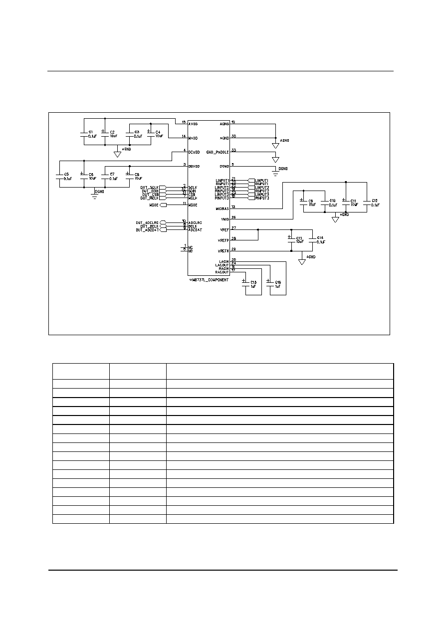
WM8737L
Preliminary Technical Data
w
AI Rev 3.0 May 2004
36
RECOMMENDED EXTERNAL COMPONENTS
Notes:
1. C1-18 should be fitted as close to WM8737 as possible.
2. AGND and DGND should be connected as close to WM8737 as possible
Figure 26 External Components Diagram
COMPONENT
REFERENCE
SUGGESTED
VALUE
DESCRIPTION
C1 100nF
Decoupling for AVDD
C2 10
�
F
Reservoir capacitor for AVDD
C3 100nF
Decoupling for MVDD
C4 10
�
F
Reservoir capacitor for MVDD
C5 100nF
Decoupling for DCVDD
C6 10
�
F
Reservoir capacitor for DCVDD
C7 100nF
Decoupling for DBVDD
C8 10
�
F
Reservoir capacitor for DBVDD
C9 100nF
Decoupling for VMID
C10 10
�
F
Reservoir capacitor for VMID
C11 100nF
Decoupling for MICBIAS
C12 10
�
F
Reservoir capacitor for MICBIAS
C9 100nF
Decoupling for VREF
C10 10
�
F
Reservoir capacitor for VREF
C11 1
�
F
RACIN to RACOUT coupling capacitor
C12 1
�
F
LACIN to LACOUT coupling capacitor
Table 23 External Components Descriptions

Preliminary Technical Data
WM8737L
w
AI Rev 3.0 May 2004
37
PACKAGE DIMENSIONS
DM030.C
FL: 32 PIN QFN PLASTIC PACKAGE 5
X
5
X
0.9 mm BODY, 0.50 mm LEAD PITCH
NOTES:
1. DIMENSION b APPLIED TO METALLIZED TERMINAL AND IS MEASURED BETWEEN 0.25 mm AND 0.30 mm FROM TERMINAL TIP. DIMENSION L1 REPRESENTS TERMINAL PULL BACK FROM
PACKAGE SIDE WALL. MAXIMUM OF 0.1mm IS ACCEPTABLE. WHERE TERMINAL PULL BACK EXISTS, ONLY UPPER HALF OF LEAD IS VISIBLE ON PACKAGE SIDE WALL DUE TO HALF
ETCHING OF LEADFRAME.
2. FALLS WITHIN JEDEC, MO-220 WITH THE EXCEPTION OF D2, E2:
D2,E2: LARGER PAD SIZE CHOSEN WHICH IS JUST OUTSIDE JEDEC SPECIFICATION
3. ALL DIMENSIONS ARE IN MILLIMETRES
4. THIS DRAWING IS SUBJECT TO CHANGE WITHOUT NOTICE.
5. SHAPE AND SIZE OF CORNER TIE BAR MAY VARY WITH PACKAGE TERMINAL COUNT. CORNER TIE BAR IS CONNECTED TO EXPOSED PAD INTERNALLY
SEE DETAIL B
E2
E2/2
b
B
16
15
A
8
9
e
5
CORNER
TIE BAR
C
0.08
C
ccc
A
A1
C
(A3)
SEATING PLANE
1
B
D2
L
D2/2
SEE DETAIL A
INDEX AREA
(D/2 X E/2)
TOP VIEW
D
C
aaa
2 X
C
aaa
2 X
E
DETAIL B
TE
RMI
N
AL TI
P
R
DA
TUM
e
e/
2
L1
1
DETAIL A
B
C
bbb
M
A
32x b
L
3
2x K
L1
R
1
1
0.
566
m
m
0.
43
m
m
5
CORNER
TIE BAR
Symbols
Dimensions (mm)
MIN
NOM
MAX
NOTE
A
A1
A3
b
D
D2
E
E2
e
L
L1
R
0.85
0.90
1.00
0.05
0.02
0
0.2 REF
0.30
0.23
0.18
5.00
3.4
3.3
3.2
0.5 BSC
0.35
0.4
0.45
0.1
b(min)/2
1
2
2
1
K
0.20
aaa
bbb
ccc
REF:
0.15
0.10
0.10
JEDEC, MO-220, VARIATION VKKD-2
Tolerances of Form and Position
4.90
5.10
5.00
4.90
5.10
3.4
3.3
3.2
EXPOSED
CENTRE
PAD
1
17
24
25
32

WM8737L
Preliminary Technical Data
w
AI Rev 3.0 May 2004
38
IMPORTANT NOTICE
Wolfson Microelectronics plc (WM) reserve the right to make changes to their products or to discontinue any product or
service without notice, and advise customers to obtain the latest version of relevant information to verify, before placing
orders, that information being relied on is current. All products are sold subject to the WM terms and conditions of sale
supplied at the time of order acknowledgement, including those pertaining to warranty, patent infringement, and limitation
of liability.
WM warrants performance of its products to the specifications applicable at the time of sale in accordance with WM's
standard warranty. Testing and other quality control techniques are utilised to the extent WM deems necessary to support
this warranty. Specific testing of all parameters of each device is not necessarily performed, except those mandated by
government requirements.
In order to minimise risks associated with customer applications, adequate design and operating safeguards must be used
by the customer to minimise inherent or procedural hazards. Wolfson products are not authorised for use as critical
components in life support devices or systems without the express written approval of an officer of the company. Life
support devices or systems are devices or systems that are intended for surgical implant into the body, or support or
sustain life, and whose failure to perform when properly used in accordance with instructions for use provided, can be
reasonably expected to result in a significant injury to the user. A critical component is any component of a life support
device or system whose failure to perform can be reasonably expected to cause the failure of the life support device or
system, or to affect its safety or effectiveness.
WM assumes no liability for applications assistance or customer product design. WM does not warrant or represent that
any license, either express or implied, is granted under any patent right, copyright, mask work right, or other intellectual
property right of WM covering or relating to any combination, machine, or process in which such products or services might
be or are used. WM's publication of information regarding any third party's products or services does not constitute WM's
approval, license, warranty or endorsement thereof.
Reproduction of information from the WM web site or datasheets is permissible only if reproduction is without alteration and
is accompanied by all associated warranties, conditions, limitations and notices. Representation or reproduction of this
information with alteration voids all warranties provided for an associated WM product or service, is an unfair and deceptive
business practice, and WM is not responsible nor liable for any such use.
Resale of WM's products or services with statements different from or beyond the parameters stated by WM for that
product or service voids all express and any implied warranties for the associated WM product or service, is an unfair and
deceptive business practice, and WM is not responsible nor liable for any such use.
ADDRESS:
Wolfson Microelectronics plc
26 Westfield Road
Edinburgh
EH11 2QB
United Kingdom
Tel :: +44 (0)131 272 7000
Fax :: +44 (0)131 272 7001
Email ::
sales@wolfsonmicro.com