Document Outline
- WM8753L
- Hi-Fi and Telephony Dual Codec
- DESCRIPTION
- FEATURES
- APPLICATIONS
- TABLE OF CONTENTS
- PIN CONFIGURATION - QFN
- PIN CONFIGURATION - BGA
- ORDERING INFORMATION
- PIN DESCRIPTION
- ABSOLUTE MAXIMUM RATINGS
- SIMULATED THERMAL PROPERTIES
- RECOMMENDED OPERATING CONDITIONS
- ELECTRICAL CHARACTERISTICS
- OUTPUT PGAêS LINEARITY
- POWER CONSUMPTION
- SIGNAL TIMING REQUIREMENTS
- CONTROL INTERFACE TIMING Ö 2-WIRE MODE
- CONTROL INTERFACE TIMING Ö 3-WIRE MODE
- AUDIO INTERFACE TIMING Ö SLAVE MODE
- AUDIO INTERFACE TIMING Ö MASTER MODE
- MODE/GPIO3 AND CSB/GPIO5 LATCH ON POWERUP TIMING
- SYSTEM CLOCK TIMING
- DEVICE DESCRIPTION
- REGISTER MAP
- POWER MANAGEMENT
- POWER SUPPLIES
- AUDIO SAMPLE RATES
- MASTER CLOCK AND PHASE LOCKED LOOP
- CONTROL INTERFACE
- AUDIO INTERFACES CONTROL
- DIGITAL AUDIO INTERFACES
- GENERAL PURPOSE INPUT/OUTPUT
- INTERRUPT CONTROLLER
- HEADPHONE OUTPUT
- HEADPHONE SWITCH
- ANALOGUE OUTPUTS
- OUTPUT SIGNAL PATH
- 3D STEREO ENHANCEMENT
- AUTOMATIC LEVEL CONTROL (ALC)
- PGA CONTROL
- INPUT SIGNAL PATH
- INTRODUCTION
- DIGITAL FILTER CHARACTERISTICS
- DAC FILTER RESPONSES
- ADC FILTER RESPONSES
- VOICE FILTER RESPONSES
- VOICE ADC FILTER RESPONSES
- VOICE DAC FILTER RESPONSES
- DE-EMPHASIS FILTER RESPONSES
- HIGHPASS FILTER
- PACKAGE DIAGRAM - 48-PIN QFN
- PACKAGE DIAGRAM - 52-PIN BGA
- IMPORTANT NOTICE
- ADDRESS:

w
WM8753L
Hi-Fi and Telephony Dual Codec
WOLFSON MICROELECTRONICS plc
www.wolfsonmicro.com
Advanced Information, June 2004, Rev 3.1
Copyright
2004 Wolfson Microelectronics plc
DESCRIPTION
The WM8753L is a low power, high quality stereo Codec with
integrated Voice CODEC designed for portable digital
telephony applications such as mobile phone, or headset with
Hi-Fi playback capability.
The device integrates dual interfaces to two differentially
connected microphones, and includes drivers for speakers,
headphone and earpiece. External component requirements
are reduced as no separate microphone or headphone
amplifiers are required, and Cap-less connections can be made
to all loads. Advanced on-chip digital signal processing
performs tone control, Bass Boost and automatic level control
for the microphone or line input through the ADC. The two
ADCs may be used to support Voice noise cancellation in a
partnering DSP, or for stereo recording.
The WM8753L Hi-Fi DAC can operate as a master or a slave,
with various master clock frequencies including 12 or 24MHz
for USB devices, 13MHz or 19.2MHz for cellular systems, or
standard 256f
s
rates like 12.288MHz and 24.576MHz. Internal
PLLs generate all required clocks for both Voice and Hi-Fi
converters. If audio system clocks already exist, the PLLs may
be committed to alternative uses.
The WM8753L operates at a nominal supply voltage of 2V,
although the digital core can operate at voltages down to 1.42V
to save power, and the maximum for all supplies is 3.6 Volts.
Different sections of the chip can also be powered down under
software control.
FEATURES
∑
Hi-Fi DAC: interfaced over I
2
S type link
∑
Audio sample rates:
8, 11.025, 16, 22.05, 24, 32, 44.1, 48, 88.2, 96
∑
DAC SNR 98dB, THD -84dB (`A' weighted @ 48kHz)
∑
ADC SNR 95dB, THD -82dB (`A' weighted @ 48kHz)
∑
On-chip Headphone Driver with cap-less output option
- 40mW output power on 16
/ 3.3V
- with
16
load: SNR 90dB, THD ≠75dB
- with
10k
load: SNR 94dB, THD ≠90dB
∑
On-chip speaker driver with 0.5W into 8R
∑
Voice Codec: interfaced over Voice interface
∑
supports sample rates from 8ks/s to 48ks/s
∑
ADC and DAC SNR 82dB, THD -74dB
∑
Two Differential Microphone Interfaces
- Dual ADCs support noise cancellation in external DSP
- Programmable ALC / Noise Gate
∑
Low-noise bias supplied for electret microphones
Other features
∑
On-chip PLLs supporting 12, 13, 19.2MHz and other clocks
∑
Cap-less connection options to headphones, earpiece, spkr.
∑
Low power, low voltage
- 1.8V to 3.6V (digital core: 1.42V to 3.6V)
- power consumption <20mW all-on with 2V supplies
- <12mW for PCM CODEC operation
∑
7x7x0.9mm QFN package, 5x5x0.9mm BGA package
APPLICATIONS
∑
MP3 Player / Recorder mobile phone
∑
Bluetooth stereo headset

Advanced Information
WM8753L
w
AI Rev 3.1 June 2004
2
TABLE OF CONTENTS
DESCRIPTION .......................................................................................................1
FEATURES ............................................................................................................1
APPLICATIONS .....................................................................................................1
TABLE OF CONTENTS .........................................................................................2
PIN CONFIGURATION - QFN ................................................................................4
PIN CONFIGURATION - BGA ...............................................................................4
ORDERING INFORMATION ..................................................................................4
PIN DESCRIPTION ................................................................................................5
ABSOLUTE MAXIMUM RATINGS.........................................................................6
SIMULATED THERMAL PROPERTIES......................................................................... 6
RECOMMENDED OPERATING CONDITIONS .....................................................6
ELECTRICAL CHARACTERISTICS ......................................................................7
TERMINOLOGY ............................................................................................................ 9
OUTPUT PGA'S LINEARITY ....................................................................................... 10
SIGNAL TIMING REQUIREMENTS .....................................................................13
SYSTEM CLOCK TIMING ........................................................................................... 13
MODE/GPIO3 AND CSB/GPIO5 LATCH ON POWERUP TIMING .............................. 13
AUDIO INTERFACE TIMING ≠ MASTER MODE......................................................... 14
AUDIO INTERFACE TIMING ≠ SLAVE MODE ............................................................ 15
CONTROL INTERFACE TIMING ≠ 3-WIRE MODE ..................................................... 16
CONTROL INTERFACE TIMING ≠ 2-WIRE MODE ..................................................... 17
DEVICE DESCRIPTION .......................................................................................18
INTRODUCTION ......................................................................................................... 18
INPUT SIGNAL PATH.................................................................................................. 20
MICROPHONE INPUTS ............................................................................................. 24
PGA CONTROL........................................................................................................... 28
AUTOMATIC LEVEL CONTROL (ALC) ....................................................................... 31
3D STEREO ENHANCEMENT .................................................................................... 34
OUTPUT SIGNAL PATH.............................................................................................. 36
ANALOGUE OUTPUTS ............................................................................................... 42
HEADPHONE SWITCH ............................................................................................... 46
HEADPHONE OUTPUT............................................................................................... 47
INTERRUPT CONTROLLER ....................................................................................... 48
GENERAL PURPOSE INPUT/OUTPUT ...................................................................... 51
DIGITAL AUDIO INTERFACES ................................................................................... 53
AUDIO INTERFACES CONTROL................................................................................ 57
CONTROL INTERFACE .............................................................................................. 61
MASTER CLOCK AND PHASE LOCKED LOOP ......................................................... 65
AUDIO SAMPLE RATES ............................................................................................. 68
POWER SUPPLIES ..................................................................................................... 70
POWER MANAGEMENT............................................................................................. 71
REGISTER MAP.......................................................................................................... 74
TERMINOLOGY .......................................................................................................... 77
DAC FILTER RESPONSES .................................................................................78
ADC FILTER RESPONSES .................................................................................79
VOICE FILTER RESPONSES ..............................................................................81
VOICE DAC FILTER RESPONSES ............................................................................. 81
VOICE ADC FILTER RESPONSES ............................................................................. 81
DE-EMPHASIS FILTER RESPONSES ................................................................82

WM8753L
Advanced Information
w
AI Rev 3.1 June 2004
3
HIGHPASS FILTER..............................................................................................83
PACKAGE DIAGRAM - 48-PIN QFN ...................................................................85
PACKAGE DIAGRAM - 52-PIN BGA...................................................................86
IMPORTANT NOTICE ..........................................................................................87
ADDRESS: .................................................................................................................. 87
Advanced Information
WM8753L
w
AI Rev 3.1 June 2004
4
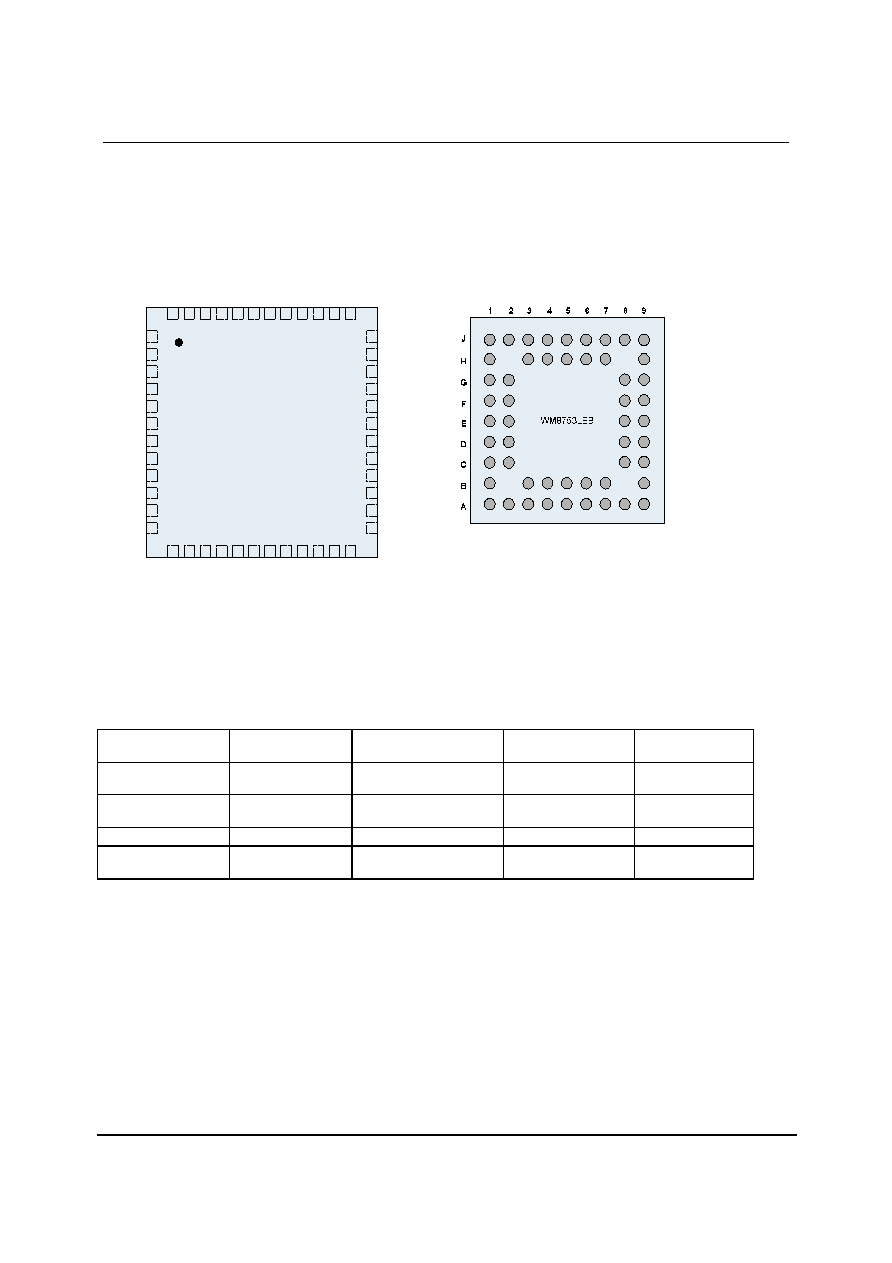
PIN CONFIGURATION - QFN
PIN CONFIGURATION - BGA
WM8753LEFL
47
46
45
48
44
43
42
41
40
39
38
37
14
15
16
13
17
18
19
20
21
22
23
24
1
2
3
4
5
6
7
8
9
10
11
12
36
35
34
33
32
31
30
29
28
27
26
25
LINE2
VXDOUT
LINE1
ACOP
RX
P
MICBIAS
VMID
VREF
AGND
AVDD
MONO1
MONO2
SPKRVDD
VXCLK
VXFS
LRC
BCLK
ADCDAT
DACDAT
MCLK
DBVDD
DCVDD
DGND
PCMCLK
SC
L
K
VX
D
I
N
CS
B
/
G
P
I
O
5
SD
I
N
MI
C
1
MI
C
1
N
RX
N
MO
D
E
/
G
PI
O
3
MI
C
2
MI
C
2
N
GP
1
/
C
L
K
1
GP
2
/
C
L
K
2
PV
D
D
PG
N
D
OU
T4
HP
V
D
D
RO
UT
1
OU
T
3
HP
/
S
P
K
RG
ND
LO
U
T
1
LO
U
T
2
RO
UT
2
GP
I
O
4
ACIN
ORDERING INFORMATION
ORDER CODE
TEMPERATURE
RANGE
PACKAGE
MOISTURE
SENSITIVITY LEVEL
PEAK SOLDERING
TEMPERATURE
WM8753LGEFL/V -25
∞
C to +85
∞
C
48-pin QFN (7x7x0.9mm)
(lead free)
MSL3 260
o
C
WM8753LGEFL/RV -25
∞
C to +85
∞
C
48-pin QFN (7x7x0.9mm)
(lead free, tape and reel)
MSL3 260
o
C
WM8753LEB/V -25
∞
C to +85
∞
C 52-pin
BGA
(5x5x0.9mm)
MSL3
240
o
C
WM8753LEB/RV -25
∞
C to +85
∞
C
52-pin BGA (5x5x0.9mm)
(tape and reel)
MSL3 240
o
C
Note:
QFN Reel quantity = 2,200
BGA Reel quantity = 3,500

WM8753L
Advanced Information
w
AI Rev 3.1 June 2004
5
PIN DESCRIPTION
BGA PIN
NO
NAME
TYPE
DESCRIPTION
J2 1 VXDOUT
Digital Output
Voice ADC Output
H3 2
VXCLK Digital Input/Output
Voice codec data clock / ADC frame clock
J3 3
VXFS Digital Input/Output
Voice Codec Frame Sync
H4 4
LRC Digital Input/Output
DAC Frame Sync
J4 5
BCLK Digital Input/Output
DAC data clock input / output
J5 6 ADCDAT
Digital Output
ADC Digital Audio Data Alternative Output
H5 7 DACDAT
Digital Input
DAC Digital Audio Data Input
J6 8
MCLK Digital Input
Master Clock Input
H6 9
DBVDD
Supply
Digital Buffer Supply (supply for digital I/O buffers)
J7 10
DCVDD Supply
Digital Core Supply (supply for digital logic, except I/O buffers)
H7 11
DGND Supply
Digital ground (all digital logic)
J8 12 PCMCLK
Digital Input
VOICE codec master clock input (may be looped from PLL output)
J9 13 GP2/CLK2
Digital Output
General Purpose Output 2, usually PLL2 output
G8 14 GP1/CLK1
Digital Output
General Purpose Output 1, usually PLL1 output
H9 15
PGND Supply PLL
ground
G9 16
PVDD Supply PLL
Supply
F9 17
HPVDD Supply Headphone
Supply
E9 18
OUT4 Analogue Output
Analogue Output 4 (Headphone driver)
E8 19
OUT3 Analogue Output
Analogue Output 3 (Headphone driver)
D9 20
ROUT1 Analogue Output
Headphone Output Right
D8 21
LOUT1 Analogue Output
Headphone Output Left
C9 22
HP/SPKRGND
Supply
Headphone and Speaker ground
B9 23
ROUT2 Analogue Output
Speaker Output Right
A9 24
LOUT2 Analogue Output
Speaker Output Left
A8 25 SPKRVDD
Supply Speaker
Supply
B7 26
MONO2 Analogue Output
Mono analogue output 2
B6 27
MONO1 Analogue Output
Mono analogue output 1
A6 28
AVDD Supply
Analogue supply (feeds ADC and DAC)
A5 29
AGND Supply
Analogue ground (feeds ADC and DAC)
B5 30
VREF Reference
Buffered ADC and DAC Reference voltage
A4 31
VMID Reference
Decoupling for ADC and DAC reference voltage
B4 32 MICBIAS
Analogue Output
Microphone Bias
A3 33
ACIN Analogue Input
AC coupled input to ALC PGA in record path
B3 34
ACOP Analogue Output
ALC Mix output
A2 35
LINE1 Analogue Input
Left Channel Input
A1 36
LINE2 Analogue Input
Right Channel input
B1 37
RXP Analogue Input
RX mono differential input positive signal
C2 38
RXN Analogue Input
RX mono differential input negative signal
C1 39
MIC1 Analogue Input
Mic Pre-amp input 1
D2 40
MIC1N Analogue Input
Mic Pre-amp 1 common mode or negative input
D1 41
MIC2 Analogue Input
Mic Pre-amp input 2
E2 42
MIC2N Analogue Input
Mic Pre-amp 2 common mode or negative input
E1 43
GPIO4 Digital input/Output
GPIO (General Purpose input/output) usually headphone jack insert
autodetect with selectable pull-up/pull-down.
F1 44 MODE/GPIO3
Digital Input / Output
Control interface Mode select on reset or GPIO3
F2 45 CSB/GPIO5
Digital Input / Output
3-wire MPU Chip Select / 2-wire MPU interface address selection or
GPIO5
G1 46
SDIN Digital Input / Output
3-wire MPU Data Input / 2-wire MPU Date Input / Acknowledge
H1 47
SCLK Digital Input
3-wire MPU Clock Input / 2-wire MPU Clock Input
J1 48
VXDIN Digital Input
VOICE DAC Input