 | –≠–ª–µ–∫—Ç—Ä–æ–Ω–Ω—ã–π –∫–æ–º–ø–æ–Ω–µ–Ω—Ç: WM8756EFT | –°–∫–∞—á–∞—Ç—å:  PDF PDF  ZIP ZIP |

WM8756
192kHz, Six Channel SACDTM Compatible Audio DAC
WOLFSON MICROELECTRONICS LTD
www.wolfsonmicro.com
Advance Information October 2001, Rev 1.3
Copyright
2001 Wolfson Microelectronics Ltd
.
DESCRIPTION
The WM8756 is a high performance 6-channel DAC
designed for audio applications such as SACDTM players,
DVD-V and DVD-A, home audio and theatre systems. The
device supports data input word lengths from 16 to 32-bits
and sampling rates up to 192kHz. The WM8756 can
implement 2 or 6 channels at 192kHz for high-end DVD-
Audio, or 6 channels at up to 192kHz for surround
applications. Additionally 64x DSD bitstream support is
offered on all 6 channels. The WM8756 consists of a serial
interface port, digital interpolation filters, multi-bit sigma
delta modulators and 6 DACs in a 48-pin TQFP package.
The WM8756 also includes a digitally controllable mute and
attenuator function on each channel, accessible during
PCM operation. An on-chip multiplexer selects between
PCM or DSD audio data input pins.
The WM8756 supports hardware or software connection
schemes for audio DAC control. The serial control interface
provides access to a wide range of features including on-
chip mute, attenuation and phase reversal. Hardware pin-
controllable operation is also available.
The WM8756 is an ideal device for all surround sound
applications supporting the SACDTM audio format, such as
SACD players, multi-format players and home
entertainment systems.
FEATURES
∑
6-Channel DAC with PCM or Bitstream (DSD) operation.
∑
DSD 64x Bitstream Support for Super Audio CDTM
∑
Independent input pins for PCM and DSD data with on-
chip multiplexer
∑
THD ≠96dB, SNR 106dB (`A' weighted @ 48kHz)
∑
PCM mode Sampling Rate: 8kHz ≠ 192kHz
∑
Master or slave operation with Normal or Phase
modulation method of DSD data transfer
∑
3-Wire Serial Control Interface
∑
Programmable PCM Audio Data Interface Modes
-
I
2
S, Left, Right Justified or DSP
-
16/20/24/32 bit Word Lengths
∑
Independent Digital Volume Control on Each Channel with
127.5dB Range in 0.5dB Steps (in PCM mode)
∑
3.0V ≠ 5.5V Supply (3.3V digital / 5V analogue option)
∑
48-pin
TQFP
Package
APPLICATIONS
∑
Super Audio CD (SACDTM) Players
∑
Universal and Multi-Format disc players
∑
Home
theatre
systems
BLOCK DIAGRAM
CONTROL
INTERFACE
DIGITAL
FILTERS
SIGMA
DELTA
MODULATOR
SIGMA
DELTA
MODULATOR
MUX
MUX
PCM/DSD
DIGITAL
FILTERS
SIGMA
DELTA
MODULATOR
SIGMA
DELTA
MODULATOR
MUX
MUX
PCM/DSD
DIGITAL
FILTERS
SIGMA
DELTA
MODULATOR
SIGMA
DELTA
MODULATOR
MUX
MUX
PCM/DSD
AUDIO
INTERFACE
PCM
DATA
DSD
DATA
LOW
PASS
FILTER
LOW
PASS
FILTER
RIGHT
DAC
LEFT
DAC
BCKIN
DSD4
DSD3
DSD2
DSD1
DSD0
DSDCLK64
DIN2
DIN1
DIN0
LRCIN
DSDCLK128
DSD5
CSB
DMCKSE
L
DMSLV
MUTE
MODE
SCKI
DSDB
MD/DM
MC/IWL
ML/I2S
OUT0R
OUT2L
GR2
OUT2R
OUT1L
GR1
OUT1R
OUT0L
GR0
LOW
PASS
FILTER
LOW
PASS
FILTER
RIGHT
DAC
LEFT
DAC
LOW
PASS
FILTER
LOW
PASS
FILTER
RIGHT
DAC
LEFT
DAC
AGND3
DGND
AVDD1
AGND1
AVDD2
AGND2
DVDD
LRCIN2

WM8756
Advance Information
AI Rev 1.3 October 2001
2
PIN CONFIGURATION
ORDERING INFORMATION
DEVICE
TEMP. RANGE
PACKAGE
WM8756EFT
-25 to +85
o
C
48-pin TQFP
nc
nc
AV
DD2
CAP
ML
/I2S
DS
DB
DG
ND
MC
/IW
L
MD
/D
M
DIN1
DSD4
DSD3
DSD2
DSD1
DSD0
DIN2
DSD5
DSDCLK64
MODE
DI
N0
DM
CKS
E
L
DV
DD
S
CKI
BCKI
N
L
RCI
N
nc
nc
AV
DD1
nc
DM
S
L
V
OUT0R
OUT1L
GR1
OUT1R
AGND3
OUT0L
GR0
OUT2L
GR2
OUT2R
AGND1
1
9
8
7
6
5
4
3
2
11
10
16 17 18 19 20 21 22
13 14 15
31
30
29
28
27
26
33
32
44 43 42 41 40 39 38
12
37
36
35
34
25
24
23
L
RCI
N2
DSDCLK128
CS
B
48 47 46 45
MUTE
AGND2
nc
nc

WM8756
Advance Information
AI Rev 1.3 October 2001
3
PIN DESCRIPTION
PIN
NAME
TYPE
DESCRIPTION
1
DIN1
Digital input
Channel 1 Serial Audio Data Input in PCM Mode.
2
DIN2
Digital input
Channel 2 Serial Audio Data Input in PCM Mode.
3
DSD0
Digital input p.d.
Channel 0 Left DSD format audio data input
4
DSD1
Digital input p.d.
Channel 0 Right DSD format audio data input
5
DSD2
Digital input p.d.
Channel 1 Left DSD format audio data input
6
DSD3
Digital input p.d.
Channel 1 Right DSD format audio data input
7
DSD4
Digital input p.d.
Channel 2 Left DSD format audio data input
8
DSD5
Digital input p.d.
Channel 2 Right DSD format audio data input
9
DSDCLK64
Digital In/Out
DSD format data clock at 64fs
10
DSDCLK128
Digital In/Out
DSD format data clock at 128fs (used in `modulated data' mode)
11
MODE
Digital input
Control Method Selection Pin in PCM Mode. `lo' = software mode
12
MUTE
Digital In/Out
Mute Control Pin in PCM Mode. `lo' = not muted
13
LRCIN2
Digital input p.d.
Second LRCIN input for dual rate mode
14
DSDB
Digital input p.u.
DSD or PCM audio data format select; `lo' = DSD mode, `hi' = PCM mode
15
DGND
Supply
Digital GND
16
ML/I2S
Digital input p.u.
Software mode: in 3-Wire Serial Control mode, Latch input.
Hardware Mode: Input Format Selection:
17
MC/IWL
Digital input p.u.
Software Mode: In 3-Wire Serial Control Mode, Clock Input.
Hardware mode: Input Word Length Selection:
18
MD/DM
Digital input
Software mode: In 3-Wire Serial Control Mode, Data Input.
Hardware mode: De-emphasis selection
19
CSB
Digital input p.d.
3-wire Serial Port Chip select ≠ active low
20
n.c.
n.c.
No internal connection
21
AVDD2
Supply
Analogue Positive DAC Reference
22
n.c.
n.c.
No internal connection
23
CAP
Analogue output
Analogue Internal Mid-Rail Reference De-Coupling Point
24
n.c.
n.c.
No internal connection
25
OUT2L
Analogue output
Left Channel 2 Output.
26
GR2
Analogue input
Channel 2 Negative Reference.
27
OUT2R
Analogue output
Right Channel 2 Output.
28
AGND1
Supply
Analogue GND
29
AGND2
Supply
Analogue GND
30
OUT1L
Analogue output
Left Channel 1 Output.
31
GR1
Analogue input
Channel 1 Negative Reference.
32
OUT1R
Analogue output
Right Channel 1 Output.
33
AGND3
Supply
Analogue GND
34
OUT0L
Analogue output
Left Channel 0 Output.
35
GR0
Analogue input
Channel 0 Negative Reference.
36
OUT0R
Analogue output
Right Channel 0 Output.
37-39
nc
nc
No internal connection
40
AVDD1
Supply
Analogue positive supply
41
nc
nc
No internal connection
42
DMSLV
Digital input p.d.
DSD mode master or slave operation select; `lo' = SLAVE (clocks are input)
43
DMCKSEL
Digital input p.d.
DSD Master Mode Clock Select (lo for 256fs; hi for 384fs)
44
DVDD
Supply
Digital Positive Supply.
45
SCKI
Digital input
Master Clock Input
46
BCKIN
Digital input
Audio Data Bit Clock Input.
47
LRCIN
Digital input
DAC Sample Rate Clock Input in PCM Mode
48
DIN0
Digital input
Channel 0 Serial Audio Data Input in PCM Mode.
Note - Digital input pins have Schmitt trigger input buffers. Pins marked `p.u.' or `p.d.' have internal pull-up or pull down.

WM8756
Advance Information
AI Rev 1.3 October 2001
4
ABSOLUTE MAXIMUM RATINGS
Absolute Maximum Ratings are stress ratings only. Permanent damage to the device may be caused by continuously operating at
or beyond these limits. Device functional operating limits and guaranteed performance specifications are given under Electrical
Characteristics at the test conditions specified.
ESD Sensitive Device. This device is manufactured on a CMOS process. It is therefore generically susceptible
to damage from excessive static voltages. Proper ESD precautions must be taken during handling and storage
of this device.
CONDITION
MIN
MAX
Digital supply voltage
-0.3V
+7V
Analogue supply voltage
-0.3V
+7V
Voltage range digital inputs
DGND -0.3V
DVDD +0.3V
Voltage range analogue inputs
AGND -0.3V
AVDD +0.3V
Master Clock Frequency
37MHz
Operating temperature range, T
A
-25
∞
C
+85
∞
C
Storage temperature
-65
∞
C
+150
∞
C
Lead temperature (soldering 10 seconds)
+240
∞
C
Lead temperature (soldering 2 minutes)
+183
∞
C
Table 1 Absolute maximum ratings

WM8756
Advance Information
AI Rev 1.3 October 2001
5
DC ELECTRICAL CHARACTERISTICS
PARAMETER
SYMBOL
TEST CONDITIONS
MIN
TYP
MAX
UNIT
Digital supply range
DVDD
3.0
5.5
V
Analogue supply range
AVDD
3.0
5.5
V
Ground
AGND, DGND
0
V
Difference of DGND to AGND
-0.3
0
+0.3
V
Difference of GR to AGND
-0.3
0
+0.3
V
Analogue supply current
AVDD = 5V
58
mA
Digital supply current
DVDD = 5V
22
mA
Analogue supply current
AVDD = 3.3V
57
mA
Digital supply current
DVDD = 3.3V
11
mA
Analogue supply current
Power down, stop clock
0.4
mA
Digital supply current
Power down, stop clock
0.09
mA
Table 2 DC electrical characteristics
Note:
1. AVDD must be equal or greater than DVDD. DVDD = 3V, AVDD = 5V is allowed.
2. Where used AVDD represents AVDD1 = AVDD2, AGND represents AGND1 = AGND2 = AGND3 and GR represents
GR0 = GR1 = GR2.
AC ELECTRICAL CHARACTERISTICS
Test Conditions
AVDD = DVDD = 3V, AGND = 0V = DGND = 0V, T
A
= +25
o
C, fs = 48kHz, SCKI = 256fs unless otherwise stated.
PARAMETER
SYMBOL
TEST CONDITIONS
MIN
TYP
MAX
UNIT
Digital Logic Levels (TTL Levels)
Input LOW level
V
IL
0.8
V
Input HIGH level
V
IH
2.0
V
Output LOW
V
OL
I
OL
= 2mA
0.4
V
Output HIGH
V
OH
I
OH
= 2mA
2.4
V
Analogue Reference Levels
Reference voltage
V
CAP
AVDD2 ≠
GR2/2
V
Potential divider resistance
R
CAP
25K
Ohms
DAC Output (Load
= 10K ohms. 50pF)
0dBFs Full scale output voltage
At DAC outputs
1.1 x
AVDD1/5
V
rms
SNR (Note 1,2,3)
A-weighted,
@ fs = 48KHz
100
106
dB
SNR (Note 1,2,3)
A-weighted
@ fs = 96KHz
98
105
dB
SNR (Note 1,2,3)
A-weighted
@ fs = 192KHz
105
dB
SNR (Note 1,2,3)
A-weighted,
@ fs = 48KHz
AVDD=DVDD=3.3V
103
dB
SNR (Note 1,2,3)
A-weighted
@ fs = 96KHz
AVDD=DVDD=3.3V
103
dB
WM8756
Advance Information
AI Rev 1.3 October 2001
6
Test Conditions
AVDD = DVDD = 3V, AGND = 0V = DGND = 0V, T
A
= +25
o
C, fs = 48kHz, SCKI = 256fs unless otherwise stated.
PARAMETER
SYMBOL
TEST CONDITIONS
MIN
TYP
MAX
UNIT
SNR (Note 1,2,3)
Non `A' weighted @ fs
= 48kHz
AVDD=DVDD=5V
103
dB
THD (Note 1,2,3)
1KHz, 0dBFs
-90
-95
dB
THD+N (Dynamic range, Note 2)
1kHz, -60dBFs
100
-106
dB
DAC channel separation
<95
dB
Analogue Output Levels
Load = 10k ohms,
0dBFS
1.1
V
rms
Output level
Load = 10k ohms,
0dBFS,
(AVDD = 3.3V)
0.73
V
rms
Gain mismatch
channel-to-channel
±1
%FSR
To midrail or a.c.
coupled
1
kOhms
Minimum resistance load
To midrail or a.c.
coupled
(AVDD = 3.3V)
1
kOhms
Maximum capacitance load
5V or 3.3V
100
pF
Output d.c. level
AVDD1-
AGND/2
V
Power On Reset (POR)
POR threshold
2.0
V
Table 3 AC Electrical Characteristics
Notes:
1. Ratio of output level with 1kHz full scale input, to the output level with all zeros into the digital input, measured `A' weighted
over a 20Hz to 20kHz bandwidth.
2. All performance measurements done with 20kHz low pass filter, and where noted an A-weight filter. Failure to use such a
filter will result in higher THD+N and lower SNR and Dynamic Range readings than are found in the Electrical
Characteristics. The low pass filter removes out of band noise; although it is not audible it may affect dynamic specification
values.
3. CAP decoupled with 10uF and 0.1uF capacitors (smaller values may result in reduced performance).

WM8756
Advance Information
AI Rev 1.3 October 2001
7
DIGITAL FILTER CHARACTERISTICS
PARAMETER
SYMBOL
TEST CONDITIONS
MIN
TYP
MAX
UNIT
Passband
±
0.05 dB
0.444fs
dB
Stopband
-3dB
0.487fs
Passband Ripple
±
0.05
dB
Stopband Attenuation
f > 0.555fs
-60
dB
Table 4 Digital Filter Characteristics ≠ PCM operation
SACD FILTER CHARACTERISTICS
With 64fs DSD data where fs = 44.1ks/s.
RESPONSE
FILTER RESPONSE WITHOUT POST-
FILTER
FILTER RESPONSE WITH 3
RD
ORDER
BUTTERWORTH POST-FILTER (-3dB AT 55KHZ)
Pass band peak ripple
0.017dB
0.017dB
Attenuation at 20kHz
-0.012dB
-0.021dB
Attenuation at 50kHz
-2.3dB
-3.9dB
Attenuation at 100kHz
-15.5dB
-31dB
Table 5 Overall frequency response in SACD mode.
TERMINOLOGY
1. Signal-to-noise ratio (dB) - SNR is a measure of the difference in level between the full scale output and the output with no
signal applied. (No Auto-zero or Automute function is employed in achieving these results).
2. Dynamic range (dB) - DNR is a measure of the difference between the highest and lowest portions of a signal. Normally a
THD+N measurement at 60dB below full scale. The measured signal is then corrected by adding the 60dB to it. (e.g.
THD+N @ -60dB= -32dB, DR= 92dB).
3. THD+N (dB) - THD+N is a ratio, of the rms values, of (Noise + Distortion)/Signal.
4. Stop band attenuation (dB) - Is the degree to which the frequency spectrum is attenuated (outside audio band).
5. Channel Separation (dB) - Also known as Cross-Talk. This is a measure of the amount one channel is isolated from the
other. Normally measured by sending a full scale signal down one channel and measuring the other.
6. Pass-Band Ripple - Any variation of the frequency response in the pass-band region.
WM8756
Advance Information
AI Rev 1.3 October 2001
8
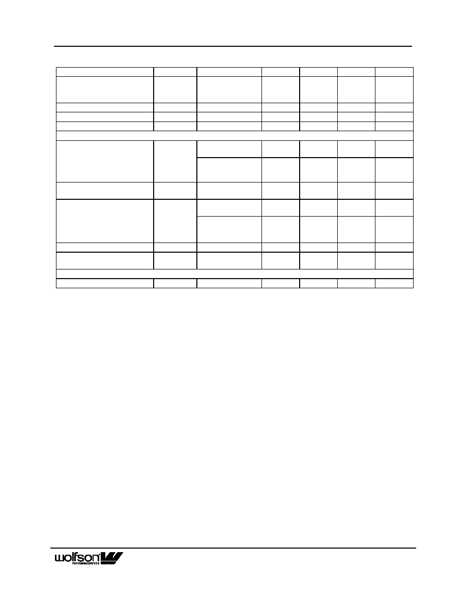
MASTER CLOCK TIMING
SCKI
t
SCKIL
t
SCKIH
t
SCKIY
Figure 1 Master Clock Timing Requirements
Test Conditions
AVDD = DVDD = 5V, AGND = GR = DGND = 0V, T
A
= +25
o
C, fs = 48kHz, SCKI = 256fs unless otherwise stated.
PARAMETER
SYMBOL
TEST CONDITIONS
MIN
TYP
MAX
UNIT
System Clock Timing Information
SCKI System clock pulse width high
t
SCKIH
13
ns
SCKI System clock pulse width low
t
SCKIL
13
ns
SCKI System clock cycle time
t
SCKIY
26
ns
SCKI Duty cycle
40:60
60:40
Table 6 Master Clock Timing Requirements
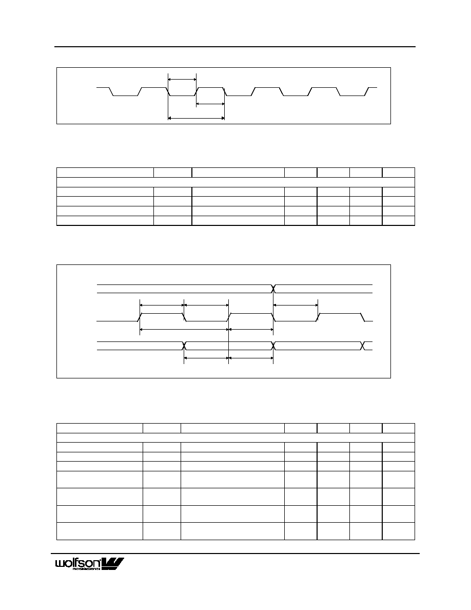
DIGITAL AUDIO INTERFACE TIMING
BCKIN
DIN0/1/2
LRCIN
t
BCH
t
BCL
t
BL
t
LB
t
BCY
t
DS
t
DH
Figure 2 PCM Digital Audio Data Timing
Test Conditions
AVDD = DVDD = 5V, AGND = GR = DGND = 0V, T
A
= +25
o
C, fs = 48kHz, SCKI = 256fs unless otherwise stated.
PARAMETER
SYMBOL
TEST CONDITIONS
MIN
TYP
MAX
UNIT
Audio Data Input Timing Information
BCKIN cycle time
t
BCY
40
ns
BCKIN pulse width high
t
BCH
16
ns
BCKIN pulse width low
t
BCL
16
ns
LRCIN set-up time to
BCKIN rising edge
t
LB
8
ns
LRCIN hold time from
BCKIN rising edge
t
BL
8
ns
DIN0/1/2 set-up time to
BCKIN rising edge
t
DS
8
ns
DIN0/1/2 hold time from
BCKIN rising edge
t
DH
8
ns
Table 7 PCM Digital Audio Timing

WM8756
Advance Information
AI Rev 1.3 October 2001
9
DSD AUDIO MONOPHASE INTERFACE
DSDCLK64
DSD[0:5]
t
DCL
t
DCH
t
DCY
t
DS
t
DH
Figure 3 DSD Audio Data Timing ≠ Normal Mode
Test Conditions
AVDD = DVDD = 5V, AGND = GR = DGND = 0V, T
A
= +25
o
C, fs = 48kHz, SCKI = 256fs unless otherwise stated.
PARAMETER
SYMBOL
TEST CONDITIONS
MIN
TYP
MAX
UNIT
Audio Data Input Timing Information
DSDCLK64 cycle time
t
DCY
354.4
ns
DSDCLK64 pulse width high
t
DCH
80
ns
DSDCLK64 pulse width low
t
DCL
80
ns
DSD[5:0] set-up time to
DSDCLK64 rising edge
t
DS
10
ns
DSD[5:0] hold time from
DSDCLK64 rising edge
t
DH
10
ns
Table 8 DSD Audio Data Timing ≠ Normal Mode

WM8756
Advance Information
AI Rev 1.3 October 2001
10
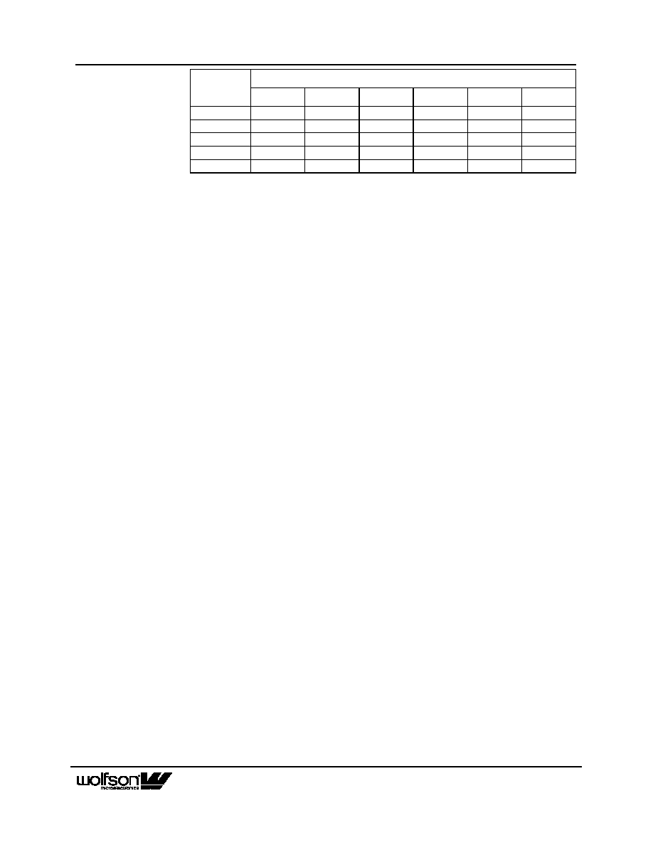
DSD AUDIO BIPHASE INTERFACE
DSDCLK128
DSD[0:5]
t
BDCH
t
BDCY128
t
BDS
D(n)
inverse D(n)
t
BDH
DSDCLK64
inverse D(n-1)
t
DIFF
t
BDCL
t
BDCY64
Figure 4 DSD Audio Data Timing - Phase Modulation Mode
Test Conditions
AVDD= DVDD = 5V, AGND= GR= DGND = 0V, T
A
= +25
o
C, fs = 48kHz, SCKI = 256fs unless otherwise stated.
PARAMETER
SYMBOL
TEST CONDITIONS
MIN
TYP
MAX
UNIT
Audio Data Input Timing Information
DSDCLK64 cycle time
t
BDCY64
354.4
ns
DSDCLK128 cycle time
t
BDCY128
177.2
ns
DSDCLK128 pulse width
high
t
BDCH
80
ns
DSDCLK128 pulse width
low
t
BDCL
80
ns
DSD[0:5] set-up time to
DSDCLK128 rising edge
t
BDS
10
ns
DSD[0:5] hold time from
DSDCLK128 rising edge
t
BDH
10
ns
Difference in edge timing of
DSDCLK64 to DSDCLK128
t
DIFF
20
ns
Table 9 DSD Digital Audio Timing

WM8756
Advance Information
AI Rev 1.3 October 2001
11
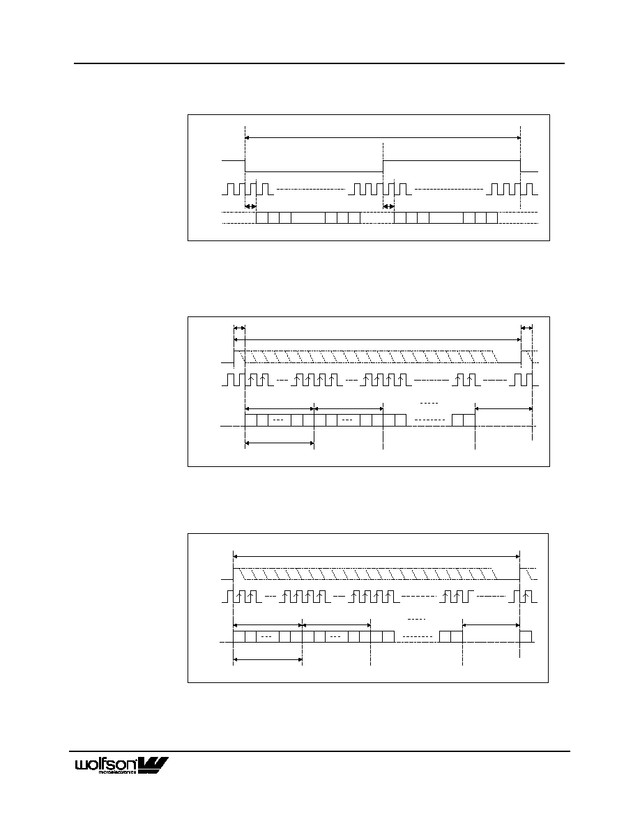
DIGITAL CONTROL INTERFACE TIMING
ML/I2S
MC/IWL
MD/DM
t
MLL
t
DHO
t
DSU
t
MLH
t
MCY
t
MCH
t
MCL
t
SCS
LSB
t
CSS
Figure 5 Control Interface Input Timing: 3-Wire Serial Control Mode
Test Conditions
AVDD= DVDD = 5V, AGND= GR= DGND = 0V, T
A
= +25
o
C, fs = 48kHz, SCKI = 256fs unless otherwise stated.
PARAMETER
SYMBOL
TEST CONDITIONS
MIN
TYP
MAX
UNIT
Program Register Input Information
MC/IWL rising edge to ML/I2S
rising edge
t
SCS
60
ns
MC/IWL pulse cycle time
t
MCY
80
ns
MC/IWL pulse width low
t
MCL
20
ns
MC/IWL pulse width high
t
MCH
20
ns
MD/DM to MC/IWL set-up time
t
DSU
20
ns
MC/IWL to MD/DM hold time
t
DHO
20
ns
ML/I2S pulse width low
t
MLL
20
ns
ML/I2S pulse width high
t
MLH
20
ns
ML/I2S rising to MC/IWL rising
t
CSS
20
ns
Table 10 Control Interface Input Timing Information

WM8756
Advance Information
AI Rev 1.3 October 2001
12
DEVICE DESCRIPTION
INTRODUCTION
WM8756 is a complete 6-channel stereo audio digital-to-analogue converter, including digital interpolation
filter, multi-bit sigma delta with dither, and switched capacitor multi-bit stereo DAC and output smoothing
filters.
The device is implemented as three separate stereo DACs in a single package and controlled by a single
interface. Each DAC has its own data input DIN0/1/2, and LRCIN, BCKIN and SCKI are shared between
them. Additionally DSD compatible bitstream operation at 64x oversampling is supported on all 6
channels. Selection of normal PCM operation or this additional DSD mode is determined by the input
level on the DSDB pin (14).
Control of internal functionality of the device is by either hardware control (pin programmed) or software
control (3-wire serial control interface). The MODE pin selects between hardware and software control. In
software control mode, a 3 wire SPI type interface is used. This interface may be asynchronous to the
audio data interface. Control data will be re-synchronized to the audio processing internally.
Operation using a system clock of 256fs, 384fs or 512fs is provided, selection between clock rates being
automatically controlled in hardware mode, or serially controlled when in software mode. Sample rates
(fs) from less than 8ks/s to 96ks/s are allowed, provided the appropriate system clock is input. Support is
also provided for up to 192ks/s using a system clock of 128fs or 192fs.
In normal PCM mode, the audio data interface supports right, left and I
2
S (Philips left justified, one bit
delayed) interface formats along with a highly flexible DSP serial port interface. When in hardware mode,
the three serial interface pins become control pins to allow selection of input data format type (I
2
S or right
justified), input word length (16, 20, 24, or 32-bit) and de-emphasis functions.
In DSD mode, a separate bitstream data input pin is required for each of the 6 channels, plus a 64fs
dataclock DSDCLK64. These signals are applied via separate pins (pins 3-9) and the signals multiplexed
internally into the DAC circuits, under control of the DSDB mode select pin (14).
Additionally in DSD mode, a Phase Modulation scheme is supported, where the audio data is transmitted
as a Manchester type, bi-phase encoded bitstream. This has the advantage of removing the significant
audio spectral energy from the datastream, so minimising digital signal corruption of the analogue
outputs. In order to simplify decoding of this phase modulated data, a 2x speed clock (DSDCLK128) is
used to sample the incoming data. This `modulated' mode is auto-detected from the presence of a clock
signal on the DSDCLK128 pin.
In DSD mode, clocks for the DAC can be inputs (WM8756 in SLAVE mode) or outputs (WM8756 in
MASTER mode). When clocks are outputs, SCKI remains an input, the lower rate clocks being derived by
dividing this master clock signal. Depending upon the setting on the DMCKSEL pin, a master clock of
either 256fs or 384fs may be used as input, from which the DSD clocks will be derived appropriately.
AUDIO DATA SAMPLING RATES
In a typical digital audio system there is only one central clock source producing a reference clock to
which all audio data processing is synchronised. This clock is often referred to as the audio system's
Master Clock. The external master system clock can be applied directly through the SCKI input pin with
no software configuration necessary. Note that on the WM8756, SCKI is used to derive clocks for the
DAC path. The DAC path consists of DAC sampling clock, DAC digital filter clock and DAC digital audio
interface timing. In a system where there are a number of possible sources for the reference clock it is
recommended that the clock source with the lowest jitter be used to optimise the performance of the
DAC.
The system clock for WM8756 supports audio sampling rates from 128fs to 768fs, where fs is the audio
sampling frequency (LRCIN) typically 32kHz, 44.1kHz, 48kHz, 96kHz or 192kHz. The system clock is
used to operate the digital filters and the noise shaping circuits.
The WM8756 has a system clock detection circuit that automatically determines the relationship between
the system clock frequency and the sampling rate (to within +/- 32 system clocks). If greater than 32
clocks error, the interface switches to 768fs and holds the output at the level of the last sample. The
system clock should be synchronised with LRCIN, although the WM8756 is tolerant of phase differences
or jitter on this clock. Table 11 shows the typical system clock frequency inputs for the WM8756.
WM8756
Advance Information
AI Rev 1.3 October 2001
13
SYSTEM CLOCK FREQUENCY (MHZ)
SAMPLING
RATE
(LRCIN)
128fs
192fs
256fs
384fs
512fs
768fs
32kHz
4.096
6.144
8.192
12.288
16.384
24.576
44.1kHz
5.6448
8.467
11.2896
16.9340
22.5792
33.8688
48kHz
6.114
9.216
12.288
18.432
24.576
36.864
96kHz
12.288
18.432
24.576
36.864
Unavailable Unavailable
192kHz
24.576
36.864
Unavailable Unavailable
Unavailable Unavailable
Table 11 System Clock Frequencies Versus Sampling Rate
DSD MODE
When pin 14, DSDB pin is held low, the device is reconfigured to operate as a DSD or `bitsteam'
compatible DAC. That is, the input audio data is in a sigma delta modulated form, or pulse density
modulated. In this case the only signals required are the bitstream for each channel supported, and the
oversampling clock.
WM8756 supports this mode when run at a 64x oversample rate. That is, the bitstream data is supplied at
a rate of 64 bits per normal word clock. Of course no word clock is provided, and the actual spectral
content of the data is determined by the noise shaping that was used to create the bitstream. WM8756
can support six channels of bitstream or DSD audio. Data BITSTREAMS and the 64fs clock are applied
to pins 3-9 and 10, if the DSDCLK128 pin is used. Signals applied to the PCM input pins 1,2, 45-48 are
ignored. The DSDB signal controls an internal multiplexor which switches the signals on the DSD input
pins into the DAC rather than the PCM signals.
In DSD mode operation, the entire digital filter on WM8756 is disabled, and the bitstream data is applied
directly to the multi-bit switched capacitor DAC's in the analogue part of the device. There, rather than
operate as oversampled multi bit DACs, the DAC inputs are reconfigured to act as analogue FIR filters, so
providing both D to A conversion of the bitstream data, and analogue smoothing of the sampled waveform
with no phase distortion. Filter responses of the analogue filter that results are shown in Figure 26 - Figure
29. Note in DSD mode software controlled functions such as digital volume control and phase reversal,
are not available. The FIR filter response is designed such that by adding only a 3
rd
order Butterworth type
post DAC filter, which may be implemented with a single op-amp, the Scarlet book specified filter
requirements may be met, saving cost over the 5
th
order filter normally needed.
It is normally desirable to use an external analogue post-DAC filter, particularly in the case of DSD
operation due to the presence of high frequency energy as a result of the aggressive high order noise
shaping used in the creation of the modulated DSD datastream. The analogue FIR filter used in WM8756
provides useful filtering of this noise, but it may be desirable to add further post filtering using active RC
filters. Figure 26 - Figure 29 show the overall filter response of the combined DAC filter operating in DSD
mode with an external 3
th
order Butterworth active RC post-DAC filter.
PCM DIGITAL AUDIO INTERFACE
PCM audio data is applied to the internal DAC filters via the PCM Digital Audio Interface. 5 popular
interface formats are supported:
∑
Left
Justified
mode
∑
Right
Justified
mode
∑
I
2
S mode
∑
DSP Early mode
∑
DSP Late mode
All 5 formats send the MSB first and support word lengths of 16, 20, 24 and 32 bits except that 32 bit data
is not supported in right justified mode. DIN0/1/2 and LRCIN are sampled on the rising, or falling edge of
BCKIN.
In left justified, right justified and I
2
S modes, the digital audio interface receives data on the DIN0/1/2
inputs. Audio Data for each stereo channel is time multiplexed with LRCIN indicating whether the left or
right channel is present. LRCIN is also used as a timing reference to indicate the beginning or end of the
data words.
In left justified, right justified and I
2
S modes, the minimum number of BCKINs per LRCIN period is 2 times
the selected word length. LRCIN must be high for a minimum of word length BCKINs and low for a

WM8756
Advance Information
AI Rev 1.3 October 2001
14
minimum of word length BCKINs. Any mark to space ratio on LRCIN is acceptable provided the above
requirements are met. The WM8756 will automatically detect when data with a LRCIN period of exactly 32
is sent, and select 16 bit mode - overriding any previously programmed word length. Word length will
revert to the previously programmed value if a LRCIN period other than 32 is detected.
In DSP early or DSP late mode, all 6 channels are time multiplexed onto DIN0. LRCIN is used as a frame
sync signal to identify the MSB of the first word. The minimum number of BCKINs per LRCIN period is 6
times the selected word length. Any mark to space ratio is acceptable on LRCIN provided the rising edge
is correctly positioned (see Figures 9 and 10).
LEFT JUSTIFIED MODE
In left justified mode, the MSB is sampled on the first rising edge of BCKIN following a LRCIN transition.
LRCIN is high during the left samples and low during the right samples.
LEFT CHANNEL
RIGHT CHANNEL
LRCIN
BCKIN
DIN0/1/2
1/fs
n
3
2
1
n-2 n-1
LSB
MSB
n
3
2
1
n-2 n-1
LSB
MSB
Figure 6 Left Justified Mode Timing Diagram
RIGHT JUSTIFIED MODE
In right justified mode, the LSB is sampled on the rising edge of BCKIN preceding a LRCIN transition.
LRCIN is high during the left samples and low during the right samples.
LEFT CHANNEL
RIGHT CHANNEL
LRCIN
BCKIN
DIN0/1/2
1/fs
n
3
2
1
n-2 n-1
LSB
MSB
n
3
2
1
n-2 n-1
LSB
MSB
Figure 7 Right Justified Mode Timing Diagram
WM8756
Advance Information
AI Rev 1.3 October 2001
15
I
2
S MODE
In I
2
S mode, the MSB is sampled on the second rising edge of BCKIN following a LRCIN transition.
LRCIN is low during the left samples and high during the right samples.
LEFT CHANNEL
RIGHT CHANNEL
LRCIN
BCKIN
DIN0/1/2
1/fs
n
3
2
1
n-2 n-1
LSB
MSB
n
3
2
1
n-2 n-1
LSB
MSB
1 BCKIN
1 BCKIN
Figure 8 I
2
S Mode Timing Diagram
DSP EARLY MODE
In DSP early mode, the first bit is sampled on the BCKIN edge following the one which detects a low to
high transition on LRCIN.
1 BCKIN
LRCIN
BCKIN
DIN0
Input Word Length (IWL)
1/fs
CHANNEL 0
LEFT
n
2
1
n-1
LSB
MSB
n
2
1
n-1
CHANNEL 0
RIGHT
2
1
CHANNEL 1
LEFT
n
n-1
CHANNEL 2
RIGHT
NO VALID DATA
1 BCKIN
Figure 9 DSP Early Mode Timing Diagram
DSP LATE MODE
In DSP late mode, the first bit is sampled on the BCKIN edge which detects a low to high transition on
LRCIN.
LRCIN
BCKIN
DIN0
Input Word Length (IWL)
1/fs
CHANNEL 0
LEFT
n
2
1
n-1
LSB
MSB
n
2
1
n-1
CHANNEL 0
RIGHT
2
1
CHANNEL 1
LEFT
n
n-1
CHANNEL 2
RIGHT
NO VALID DATA
1
Figure 10 DSP Late Mode Timing Diagram
In both early and late DSP modes, DAC0 left is always sent first, followed immediately by data words for
the other 5 channels. No BCKIN edges are allowed between the data words. The word order is DAC0 left,
DAC0 right, DAC1 left, DAC1 right, DAC2 left, DAC2 right.

WM8756
Advance Information
AI Rev 1.3 October 2001
16
SPLIT RATE MODE
The WM8756 can be used with differing sample rates on the front and rear channels. This allows
extremely high quality audio to be played on the front two channels whilst the other channels use normal
high quality data streams.
This mode will only work with a front data rate of 192kHz and a rear rate of 96kHz but can be used with all
the normal data formats except the two DSP modes and with the system at either 128fs or 192fs see
Figure 11.
When running in split rate mode all the channels are clocked in using a common BCKIN; the front
channels using LRCIN and all the other channels using LRCIN2 see Figure 11.
LEFT CHANNEL
RIGHT CHANNEL
LRCIN
BCKIN
DIN0
2/fs
LSB
MSB
LSB
MSB
LEFT CHANNEL
RIGHT CHANNEL
n
2
1
n
2
1
n
2
1
n
2
1
LSB
MSB
LSB
MSB
n
2
1
n
2
1
MSB
LSB
LSB
MSB
DIN1/2
LRCIN2
LEFT CHANNEL
RIGHT CHANNEL
Figure 11 Split Rate Audio Mode Timing Diagram
Notes:
1. Figure 11 shows the timing for left justified. However, this is similar for right justified and I2S.
2. The edges of LRCIN and LRCIN2 must be coincidental.

WM8756
Advance Information
AI Rev 1.3 October 2001
17
MODES OF OPERATION
Control of the various modes of operation for the WM8756 is either by software control over the serial interface, or by hard-
wired pin control. Selection of software or hardware mode is via the MODE pin. The following functions may be controlled
either via the serial control interface or by hard wiring of the appropriate pins.
Note : In DSD mode, the control interface is available but none of the functions will have any effect except the PDWN bit
because the DSD data by-passes the majority of the signal processing.
FUNCTION
OPTIONS
SOFTWARE CONTROL
DEFAULT VALUE
PIN 11: MODE = 0
HARDWARE CONTROL
BEHAVIOUR
PIN 11: MODE = 1
Input audio data format
Right justified
Left justified
I
2
S format
DSP formats
FMT = 00 (default)
FMT = 01
FMT = 10
FMT = 11
Pin 16, 17: ML/I2S, MC/IWL = 00, 01 or 10
Not available in hardware mode
Pin 16, 17: ML/I2S, MC/IWL = 11
Not available in hardware mode
Input word length
16
20
24
32
IWL[1:0] = 00
IWL[1:0] = 01
IWL[1:0] = 10 (default)
IWL[1:0] = 11
Pin 16, 17: ML/I2S, MC/IWL = 00 (RJ)
Pin 16, 17: ML/I2S, MC/IWL = 01 (RJ)
Pin 16, 17: ML/I2S, MC/IWL = 10 (RJ)
Pin 16, 17: ML/I2S, MC/IWL = 11 (I
2
S)
De-emphasis selection
On
Off
DEEMPH = 1
DEEMPH = 0 (Default)
Pin 18: MD/DM = 1
Pin 18: MD/DM = 0
Mute
On
Off
MUTE = 1
MUTE = 0 (default)
Pin 12: MUTE = 1
Pin 12: MUTE = 0
Input LRCIN polarity
Normal
Inverted
LRP = 0 (default)
LRP = 1
Not available in hardware mode,
default value set
Volume control
Lch, Rch
individually
Lch, Rch
common
ATC = 0; 0dB (default)
ATC = 1
Not available in hardware mode,
gain defaults to 0dB
Infinite zero detect
On
Off
IZD = 1
IZD = 0 (default)
Automute function controlled from MUTE pin
low = never mute
floating = automute enable
high = mute
Power down
Chip on
Chip off
PDWN = 0 (default)
PDWN = 1
Run SCKI
Stop SCKI
DAC output control
See Table 13
for all options
Default is PL[3:0] = 1001, stereo mode
Not available in hardware mode
Table 12 Control Function Summary

WM8756
Advance Information
AI Rev 1.3 October 2001
18
SOFTWARE CONTROL MODES
DIGITAL AUDIO INTERFACE CONTROL REGISTERS
Interface format is selected via the FMT[1:0] register bits:
REGISTER ADDRESS
BIT
LABEL
DEFAULT
DESCRIPTION
0000011
Interface Control
1:0
FMT[1:0]
00
Interface format Select
00 : right justified mode
01: left justified mode
10: I2S mode
11: DSP (early or late) mode
In left justified, right justified or I2S modes, the LRP register bit controls the polarity of LRCIN. If this bit is
set high, the expected polarity of LRCIN will be the opposite of that shown in Figure 6, Figure 7 and
Figure 8. Note that if this feature is used as a means of swapping the left and right channels, a 1 sample
phase difference will be introduced.
REGISTER ADDRESS
BIT
LABEL
DEFAULT
DESCRIPTION
0000011
Interface Control
2
LRP
0
LRCIN Polarity
0 : normal LRCIN polarity
1: inverted LRCIN polarity
In DSP modes, the LRCIN register bit is used to select between early and late modes:
REGISTER ADDRESS
BIT
LABEL
DEFAULT
DESCRIPTION
0000011
Interface Control
2
LRP
0
DSP Format
0 : Early DSP mode
1: Late DSP mode
By default, LRCIN and DIN0/1/2 are sampled on the rising edge of BCKIN and should ideally change on
the falling edge. Data sources which change LRCIN and DIN0/1/2 on the rising edge of BCKIN can be
supported by setting the BCP register bit. Setting BCP to 1 inverts the polarity of BCKIN to the inverse of
that shown in Figures 6, 7 and 8.
REGISTER ADDRESS
BIT
LABEL
DEFAULT
DESCRIPTION
0000011
Interface Control
3
BCP
0
BCKIN Polarity
0 : normal BCKIN polarity
1: inverted BCKIN polarity
The IWL[1:0] bits are used to control the input word length.
REGISTER ADDRESS
BIT
LABEL
DEFAULT
DESCRIPTION
0000011
Interface Control
5:4
IWL[1:0]
10
Input Word Length
00 : 16 bit data
01: 20 bit data
10: 24 bit data
11: 32 bit data
Note: If 32-bit mode is selected in right justified mode, the WM8756 defaults to 24 bits.
In all modes, the data is signed 2's complement. The digital filters always input 24-bit data. If the DAC is
programmed to receive 16 or 20 bit data, the WM8756 pads the unused LSBs with zeros. If the DAC is
programmed into 32 bit mode, the 8 LSBs are ignored.

WM8756
Advance Information
AI Rev 1.3 October 2001
19
The REV[2:0] bits are used to invert the phase of the DAC outputs. REV0 controls phase of DAC0, REV1
controls phase of DAC1 and REV2 controls phase of DAC2.
REGISTER ADDRESS
BIT
LABEL
DEFAULT
DESCRIPTION
0000011
Interface Control
8:6
REV[2:0]
000
Output phase direction
1 in bit 6 reverses OUT0L/R.
1 in bit 7 reverses OUT1L/R.
1 in bit 8 reverses OUT2L/R.
MUTE MODES
Setting the MUTE register bit will apply a 'soft' mute to the input of the digital filters:
REGISTER ADDRESS
BIT
LABEL
DEFAULT
DESCRIPTION
0000010
DAC Channel Control
0
MUTE
0
Soft Mute select
0 : Normal Operation
1: Soft mute all channels
-2.5
-2
-1.5
-1
-0.5
0
0.5
1
1.5
0
0.001
0.002
0.003
0.004
0.005
0.006
Time(s)
Figure 12 Application and Release of Soft Mute
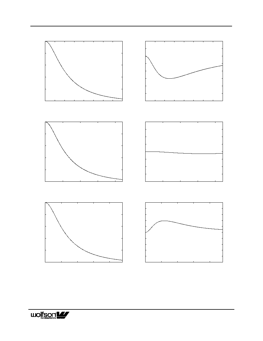
Figure 12 shows the application and release of MUTE whilst a full amplitude sinusoid is being played at
48kHz sampling rate. When MUTE (lower trace) is asserted, the output (upper trace) begins to decay
exponentially from the DC level of the last input sample. The output will decay towards V
CAP
with a time
constant of approximately 64 input samples. If MUTE is applied for 1024 or more input samples, the
outputs will be connected directly to V
CAP
- this feature can be disabled using the IZD (infinite zero detect)
bit. When MUTE is de-asserted, the output will restart almost immediately from the current input sample.
Note that all other means of muting the DAC channels (setting the PL[3:0] bits to 0, setting the PDWN bit
or setting attenuation to 0) will cause much more abrupt muting of the output.
Setting the IZD register bit will enable the internal analogue mute feature:
REGISTER ADDRESS
BIT
LABEL
DEFAULT
DESCRIPTION
0000010
DAC Channel Control
4
IZD
0
Internal Analogue Mute Disable
0 : Disable Analogue Mute
1: Enable Analogue Mute

WM8756
Advance Information
AI Rev 1.3 October 2001
20
With IZD enabled, applying MUTE for 1024 consecutive input samples will cause all outputs to be
connected directly to V
CAP
. Additionally, if 2048 consecutive zero input samples are applied to all 6
channels, and IZD=0, internal analogue mute will be applied. It will be removed as soon as any channel
receives a non-zero input.
The MUTE pin can be used as an input. In this case it performs the same function as the MUTE register
bit. Driving the MUTE pin high will apply a 'soft' mute. Driving it low again, will remove the MUTE
immediately. Note that this hardware mute feature doesn't require the MODE pin to be set high.
MUTE PIN
DESCRIPTION
0
Normal Operation
1
Mute all DAC channels
floating
Enable IZD, Mute becomes an output to indicate when IZD occurs.
A diagram showing how the various Mute modes interact is shown below in Figure 13.
IZD (Register Bit)
AUTOMUTED
(Internal Signal)
10k
MU (Register Bit)
SOFTMUTE
(Internal
Signal)
MUTE
PIN
Figure 13 Selection Logic for MUTE Modes
The MUTE pin behaves as a bi-directional function, that is, as an input to select MUTE or NOT-MUTE, or
as an output indication of automute operation. MUTE is active high; taking the pin high causes the filters
to soft mute, ramping down the audio signal over a few milliseconds. Taking MUTE low again allows data
into the filter.
The automute function detects a series of zero value audio samples of 1024 samples long being applied
to all 6 channels. After such an event, a latch is set whose output (AUTOMUTED) is wire OR'ed through a
10kohm resistor to the MUTE pin. Thus if the MUTE pin is not being driven, the automute function will
assert MUTE.
If MUTE is tied low, AUTOMUTED is overridden and will not mute. If MUTE is driven from a source
follower, or diode, then both MUTE and automute functions are available. If MUTE is not driven,
AUTOMUTED appears as a weak output (10k source impedance) so can be used to drive external mute
circuits. The automute signal is AND'ed with IZD, this qualified mute signal then being OR'ed into the
SOFTMUTE control. Therefore, in software mode, automute operation may be controlled with IZD control
bit.

WM8756
Advance Information
AI Rev 1.3 October 2001
21
DE-EMPHASIS MODE
Setting the DEEMPH register bit puts the all the digital filters into de-emphasis mode:
REGISTER ADDRESS
BIT
LABEL
DEFAULT
DESCRIPTION
0000010
DAC Channel Control
1
DEEMPH
0
De-emphasis mode select:
0 : Normal Mode
1: De-emphasis Mode
Refer to Figure 20 - Figure 25 for details of the De-Emphasis filtering effects at different sample rates.
In hardware mode (MODE=1) driving the MD/DM pin high has the same effect as setting the DEEMPH bit:
MODE PIN
MD/DM PIN
DESCRIPTION
0
ignored
De-Emphasis controlled from DEEMPH register bit
1
0
Normal Mode
1
1
De-Emphasis Mode
POWERDOWN MODE
Setting the PDWN register bit immediately connects all outputs to V
CAP
and selects a low power mode.
All trace of the previous input samples is removed, but all control register settings are preserved. When
PDWN is cleared again the first 16 input samples will be ignored as the FIR will repeat it's power-on
initialisation sequence.
REGISTER ADDRESS
BIT
LABEL
DEFAULT
DESCRIPTION
0000010
DAC Channel Control
2
PDWN
0
Power Down Mode Select:
0 : Normal Mode
1: Power Down Mode
ATTENUATOR CONTROL MODE
Setting the ATC register bit causes the left channel attenuation settings to be applied to both left and right
channels for all three pairs of DACs from the next audio input sample. No update to the attenuation
registers is required for ATC to take effect.
REGISTER ADDRESS
BIT
LABEL
DEFAULT
DESCRIPTION
0000010
DAC Channel Control
3
ATC
0
Attenuator Control Mode:
0 : Right channels use Right
attenuations
1: Right Channels use Left
Attenuations

WM8756
Advance Information
AI Rev 1.3 October 2001
22
DAC OUTPUT CONTROL
The DAC output control word determines how the left and right inputs to the audio Interface are applied to
the left and right DACs:
REGISTER ADDRESS
BIT
LABEL
DEFAULT
DESCRIPTION
PL[3:0]
Left
Output
Right
Output
0000
Mute
Mute
0001
Left
Mute
0010
Right
Mute
0011
(L+R)/2
Mute
0100
Mute
Left
0101
Left
Left
0110
Right
Left
0111
(L+R)/2
Left
1000
Mute
Right
1001
Left
Right
1010
Right
Right
1011
(L+R)/2
Right
1100
Mute
(L+R)/2
1101
Left
(L+R)/2
1110
Right
(L+R)/2
0000010
DAC Control
8:5
PL[3:0]
1001
1111
(L+R)/2
(L+R)/2
Table 13 Input to output control

WM8756
Advance Information
AI Rev 1.3 October 2001
23
ATTENUATION CONTROL (ONLY APPLICABLE TO PCM MODE)
Each DAC channel can be attenuated digitally before being applied to the digital filter. Attenuation is 0dB
by default but can be set between 0 and 127.5dB in 0.5dB steps using the 7 Attenuation control words. All
attenuation registers are double latched allowing new values to be pre-latched to several channels before
being updated synchronously. Setting the UPDATE bit on any attenuation write will cause all pre-latched
values to be immediately applied to the DAC channels. A master attenuation register is also included,
allowing all attenuations to be set to the same value in a single write.
REGISTER
ADDRESS
BIT
LABEL
DEFAULT
DESCRIPTION
7:0
L0A[7:0]
11111111
(0dB)
Attenuation level of left channel DACL0 in 0.5dB steps, see Table 15
Attenuation Control Levels.
0000
Attenuation
DACL0
8
UPDATE
Not latched
Controls simultaneous update of all Attenuation Latches
0: Store DACL0 in intermediate latch (no change to output)
1: Store DACL0 and update attenuation on all channels.
7:0
R0A[7:0]
11111111
(0dB)
Attenuation level of right channel DACR0 in 0.5dB steps, see Table 15
Attenuation Control Levels.
0001
Attenuation
DACR0
8
UPDATE
Not latched
Controls simultaneous update of all Attenuation Latches
0: Store DACR0 in intermediate latch (no change to output)
1: Store DACR0 and update attenuation on all channels.
7:0
L1A[7:0]
11111111
(0dB)
Attenuation level of left channel DACL1 in 0.5dB steps, see Table 15
Attenuation Control Levels.
0100
Attenuation
DACL1
8
UPDATE
Not latched
Controls simultaneous update of all Attenuation Latches
0: Store DACL1 in intermediate latch (no change to output)
1: Store DACL1 and update attenuation on all channels.
7:0
R1A[7:0]
11111111
(0dB)
Attenuation level of right channel DACR1 in 0.5dB steps, see Table 15
Attenuation Control Levels.
0101
Attenuation
DACR1
8
UPDATE
Not latched
Controls simultaneous update of all Attenuation Latches
0: Store DACR1 in intermediate latch (no change to output)
1: Store DACR1 and update attenuation on all channels.
7:0
L2A[7:0]
11111111
(0dB)
Attenuation level of left channel DACL2 in 0.5dB steps, see Table 15
Attenuation Control Levels.
0110
Attenuation
DACL2
8
UPDATE
Not latched
Controls simultaneous update of all Attenuation Latches
0: Store DACL2 in intermediate latch (no change to output)
1: Store DACL2 and update attenuation on all channels.
7:0
R2A[7:0]
11111111
(0dB)
Attenuation level of right channel DACR2 in 0.5dB steps, see Table 15
Attenuation Control Levels.
0111
Attenuation
DACR2
8
UPDATE
Not latched
Controls simultaneous update of all Attenuation Latches
0: Store DACR2 in intermediate latch (no change to output)
1: Store DACR2 and update attenuation on all channels.
7:0
MASTA[7:0]
11111111
(0dB)
Attenuation of all channels in 0.5dB steps, see Table 15 Attenuation
Control Levels.
1000
Master
Attenuation
(all channels)
8
UPDATE
Not latched
Controls simultaneous update of all Attenuation Latches
0: Store MASTA[7:0] in all intermediate latches (no change)
1: Store MASTA[7:0] and update attenuation on all channels.
Table 14 Attenuation Register Map
Notes:
1.
The UPDATE bit is not latched. If UPDATE=0, the Attenuation value will be written to the pre-latch but not applied to the
relevant DAC. If UPDATE=1, all pre-latched values will be applied from the next input sample. Writing to MASTA[7:0] overwrites
any values previously sent to L0A[7:0], L1A[7:0], L2A[7:0], R0A[7:0], R1A[7:0], R2A[7:0].
2.
The attenuation level is only applied when the input data passes through midrail unless the ZCD function (register 9, bit 1) is
disabled where it will change immediately.
WM8756
Advance Information
AI Rev 1.3 October 2001
24
DAC OUTPUT ATTENUATION
Register bits [7:0] of L0A and R0A control the left and right channel attenuation of DAC 0. Register bits
[7:0] of L1A and R1A control the left and right channel attenuation of DAC 1. Register bits [7:0] of L2A and
R2A control the left and right channel attenuation of DAC 2. Register bits [7:0] of MASTA are a register
that can be used to control attenuation of all channels.
Table 15 shows how the attenuation levels are selected from the 8-bit words.
AX[7:0]
ATTENUATION LEVEL
00(hex)
-
dB (mute)
01(hex)
-127.5dB
:
:
:
:
:
:
FE(hex)
-0.5dB
FF(hex)
0dB
Table 15 Attenuation Control Levels
EXTENDED INTERFACE CONTROL
It is possible to run the WM8756 channels at different rates with the front two channels running at twice
the rate of the rear four channels. In this mode which is enabled by bit 0 of register 9, the interface runs
at the faster data rate but pin 13 acts as the framing LRCIN for the rear channels see Figure 11.
REGISTER ADDRESS
BIT
LABEL
DEFAULT
DESCRIPTION
0001001
Split rate mode
0
2SPD
0
Activates the split rate mode
0: Normal operation.
1: Split rate operation.
When the WM8756 receives updates to the volume levels it will, by default, wait for the signal to pass
through midrail before applying the change to the output. This ensures that minimal distortion is seen on
the output when the volume is changed. This function applies individually to each channel.
REGISTER ADDRESS
BIT
LABEL
DEFAULT
DESCRIPTION
0001001
Zero crossing detect
1
ZCD
0
Controls the ZCD
0: Enabled.
1: Disabled.

WM8756
Advance Information
AI Rev 1.3 October 2001
25
HARDWARE CONTROL MODES
When the MODE pin is held high, and DSDB pin is high, the following hardware modes of operation are
available.
MUTE AND AUTOMUTE OPERATION
In both hardware and software modes pin 12 (MUTE) controls selection of MUTE directly, and can be
used to enable and disable the automute function, or as an output of the automuted signal.
AUTOMUTED (Internal
Signal)
10k
SOFTMUTE
(Internal
Signal)
MUTE
PIN
Figure 14 Mute Circuit Operation
The MUTE pin behaves as a bi-directional function, that is, as an input to select MUTE or NOT-MUTE, or
as an output indication of automute operation. MUTE is active high; taking the pin high causes the filters
to soft mute, ramping down the audio signal over a few milliseconds. Taking MUTE low again allows data
into the filter.
The automute function detects a series of zero value audio samples of 1024 samples long being applied
to all 6 channels. After such an event, a latch is set whose output (AUTOMUTED) is wire OR'ed through a
10kohm resistor to the MUTE pin. Thus if the MUTE pin is not being driven, the automute function will
assert MUTE.
If MUTE is tied low, AUTOMUTED is overridden and will not mute. If MUTE is driven from a source
follower, or diode, then both MUTE and automute functions are available. If MUTE is not driven,
AUTOMUTED appears as a weak output (10k source impedance) so can be used to drive external mute
circuits.
INPUT FORMAT SELECTION
In hardware mode, pins 16 and 17 become input controls for selection of input data format type and input
data word length (see Table 16). I
2
S mode is designed to support any word length provided enough bit
clocks are sent.
ML/I2S
MC/IWL
INPUT DATA MODE
0
0
16-bit right justified
0
1
20-bit right justified
1
0
24-bit right justified
1
1
I
2
S mode
Table 16 Control of Input Data Format Type and Input Data Word Length
MD/DM DE-EMPHASIS
In hardware mode, pin 18 becomes an input control for selection of de-emphasis filtering to be applied
(see Table 17).
MD/DM
DE-EMPHASIS MODE
0
De-emphasis off
1
De-emphasis on
Table 17 De-emphasis Control

WM8756
Advance Information
AI Rev 1.3 October 2001
26
DSDB MODE SELECT
This pin puts the device into DSD mode when taken low. Due to the nature of DSD operation only a single
software controlled function is available in this mode. This is the PDWN bit.
DSDB
DSD MODE
0
Device in DSD mode
1
Device in normal PCM operation
Table 18 DSD mode Control
DSD DIGITAL AUDIO INTERFACE
DSD mode is selected by taking the DSDB pin low. In this mode the internal digital filters are by-passed,
and the already modulated bitstream data is applied directly to the Switched Capacitor DAC filter where it
is converted and low-pass filtered.
Two formats are supported for data transfer, NORMAL or PHASE MODULATED.
In Normal mode, DSD data is simply clocked into the device using the rising edge of the 64fs DSDCLK64
signal (see Figure 3).
In Phase Modulation mode, the data is supplied in Manchester encoded form (a bit transition occurs
during every data bit, which shapes the spectral energy minimising corruption of the analogue outputs). A
secondary clock DSDCLK128, at 128fs is used to simplify data recovery, the data simply being clocked
with the falling edge of DSDCLK128 when DSDCLK64 is low (see Figure 4). Operation of PHASE
MODULATED mode is auto-detected by the presence of a clock signal on the DSDCLK128 pin.
DSD clocks are either inputs (when DMSLV = `0') or outputs (when DMSLV = `1'). When DMSLV is `1' the
clocks are derived by using the SCKI as detailed below:
DMCKSEL
DSDCLK64
DSDCLK128
0
SCKI/4
SCKI/2
1
SCKI/6
SCKI/3
Table 19 Master/Slave clock selection
DMSLV
CLOCKS
0
inputs
1
outputs
Table 20 Master/Slave function
See Figure 3 and Figure 4 for details of DSD interface timing

WM8756
Advance Information
AI Rev 1.3 October 2001
27
SOFTWARE CONTROL INTERFACE
The software control interface uses a 3-wire serial control interface. Selection of interface format is
achieved by setting the state of the MODE pin.
MODE
INTERFACE FORMAT
0
Software Control Mode
1
Hardware Control Mode
Table 21 Control Interface Mode Selection
3-WIRE (SPI COMPATIBLE) SERIAL CONTROL MODE
The WM8756 can be controlled using a 3-wire serial interface. MD/DM is used for the program data,
MC/IWL is used to clock in the program data and ML/I2S is use to latch in the program data. The 3-wire
interface protocol is shown in Figure 15.
ML/I2S
MC/IWL
MD/DM
D6
D7
D8
A0
A1
A2
A3
A4
D1
D2
D3
D4
D5
D0
A5
A6
Figure 15 3-wire Serial Interface
Notes:
1. A[6:0] are Control Address Bits
2. D[8:0] are Control Data Bits

WM8756
Advance Information
AI Rev 1.3 October 2001
28
REGISTER MAP
There are 9 registers with 9 bits per register. These can be controlled using the Control Interface.Table 22 below gives an overview of
all the WM8756 control registers. Details of each register's function are summarised on the following pages (Table 23).
A6
A5
A4
A3
A2
A1
A0
D8
D7
D6
D5
D4
D3
D2
D1
D0
M0
0
0
0
0
0
0
0
UPDATE
L0A7
L0A 6
L0A 5
L0A 4
L0A 3
L0A 2
L0A 1
L0A 0
M1
0
0
0
0
0
0
1
UPDATE
R0A7
R0A 6
R0A 5
R0A 4
R0A 3
R0A 2
R0A 1
R0A 0
M2
0
0
0
0
0
1
0
PL3
PL2
PL1
PL0
IZD
ATC
PDWN
DEEMPH
MUTE
M3
0
0
0
0
0
1
1
REV2
REV1
REV0
IWL1
IWL0
BCP
LRP
FMT1
FMT0
M4
0
0
0
0
1
0
0
UPDATE
L1A7
L1A 6
L1A 5
L1A 4
L1A 3
L1A 2
L1A 1
L1A 0
M5
0
0
0
0
1
0
1
UPDATE
R1A7
R1A 6
R1A 5
R1A 4
R1A 3
R1A 2
R1A 1
R1A 0
M6
0
0
0
0
1
1
0
UPDATE
L2A7
L2A 6
L2A 5
L2A 4
L2A 3
L2A 2
L2A 1
L2A 0
M7
0
0
0
0
1
1
1
UPDATE
R2A7
R2A 6
R2A 5
R2A 4
R2A 3
R2A 2
R2A 1
R2A 0
M8
0
0
0
1
0
0
0
UPDATE
MASTA7
MASTA 6
MASTA 5
MASTA 4
MASTA 3
MASTA 2
MASTA 1
MASTA 0
M9
0
0
0
1
0
0
1
0
0
0
0
0
0
0
ZCD
2SPD
Table 22 Register Map

WM8756
Advance Information
AI Rev 1.3 October 2001
29
REGISTER
ADDRESS
BIT
LABEL
DEFAULT
DESCRIPTION
7:0
L0A[7:0]
11111111
(0dB)
Attenuation level of left channel DACL0 in 0.5dB steps, see Table 15
Attenuation Control Levels.
0000000
Attenuation
DACL0
8
UPDATE
Not latched
Controls simultaneous update of all Attenuation Latches
0: Store DACL0 in intermediate latch (no change to output)
1: Store DACL0 and update attenuation on all channels.
7:0
R0A[7:0]
11111111
(0dB)
Attenuation level of right channel DACR0 in 0.5dB steps, see Table 15
Attenuation Control Levels.
0000001
Attenuation
DACR0
8
UPDATE
Not latched
Controls simultaneous update of all Attenuation Latches
0: Store DACR0 in intermediate latch (no change to output)
1: Store DACR0 and update attenuation on all channels.
0
MUTE
0
Left and Right DACs soft mute control
0: No Mute
1: Mute
1
DEEMPH
0
De-emphasis Control
0: Normal Response (see Figure 16 - Figure 19)
1: De-emphasis Response (see Figure 20 - Figure 25)
2
PDWN
0
Left and Right DACs Power-down Control
0: All DACs running, output is active
1: All DACs in power saving mode, output muted
3
ATC
0
Attenuator Control
0: All DACs use attenuations as programmed.
1: Right chan. DACs use corresponding left DAC attenuations
4
IZD
0
Infinite zero detection circuit control and automute control
0: Infinite zero detect disabled
1: Infinite zero detect enabled
DAC Output Control
PL[3:0]
Left
Output
Right
Output
PL[3:0]
Left
Output
Right
Output
0000
Mute
Mute
1000
Mute
Right
0001
Left
Mute
1001
Left
Right
0010
Right
Mute
1010
Right
Right
0011
(L+R)/2
Mute
1011
(L+R)/2
Right
0100
Mute
Left
1100
Mute
(L+R)/2
0101
Left
Left
1101
Left
(L+R)/2
0110
Right
Left
1110
Right
(L+R)/2
0000010
DAC Control
8:5
PL[3:0]
1001
0111
(L+R)/2
Left
1111
(L+R)/2
(L+R)/2

WM8756
Advance Information
AI Rev 1.3 October 2001
30
1:0
FMT[1:0]
00
Interface format select
00: right justified mode
01: left justified mode
10: I2S mode
11: DSP mode
LRCIN Polarity or LRCIN Phase
2
LRP
0
Left Justified / Right Justified / I2S
0: Standard LRCIN Polarity
1: Inverted LRCIN Polarity
DSP Mode
0: DSP early mode
1: DSP late mode
3
BCP
0
BCKIN Polarity
0: Normal (DIN[2:0] and LRCIN sampled on rising edge)
1: Inverted (DIN[2:0] and LRCIN sampled on falling edge)
5:4
IWL[1:0]
0
Input Word Length
00: 16-bit Mode
01: 20-bit Mode
10: 24-bit Mode
11: 32-bit Mode (not supported in right justified mode)
0000011
Interface
Control
8:6
REV[2:0]
000
Controls the output phase of the three stereo channels
1 in bit 6 reverses the phase of data output on OUT0L/R.
1 in bit 7 reverses the phase of data output on OUT1L/R.
1 in bit 8 reverses the phase of data output on OUT2L/R.
7:0
L1A[7:0]
11111111
(0dB)
Attenuation level of left channel DACL1 in 0.5dB steps, see Table 15
Attenuation Control Levels.
0000100
Attenuation
DACL1
8
UPDATE
Not latched
Controls simultaneous update of all Attenuation Latches
0: Store DACL1 in intermediate latch (no change to output)
1: Store DACL1 and update attenuation on all channels.
7:0
R1A[7:0]
11111111
(0dB)
Attenuation level of right channel DACR1 in 0.5dB steps, see Table 15
Attenuation Control Levels.
0000101
Attenuation
DACR1
8
UPDATE
Not latched
Controls simultaneous update of all Attenuation Latches
0: Store DACR1 in intermediate latch (no change to output)
1: Store DACR1 and update attenuation on all channels.
7:0
L2A[7:0]
11111111
(0dB)
Attenuation level of left channel DACL2 in 0.5dB steps, see Table 15
Attenuation Control Levels.
0000110
Attenuation
DACL2
8
UPDATE
Not latched
Controls simultaneous update of all Attenuation Latches
0: Store DACL2 in intermediate latch (no change to output)
1: Store DACL2 and update attenuation on all channels.
7:0
R2A[7:0]
11111111
(0dB)
Attenuation level of right channel DACR2 in 0.5dB steps, see Table 15
Attenuation Control Levels.
0000111
Attenuation
DACR2
8
UPDATE
Not latched
Controls simultaneous update of all Attenuation Latches
0: Store DACR2 in intermediate latch (no change to output)
1: Store DACR2 and update attenuation on all channels.
7:0
MASTA[7:0]
11111111
(0dB)
Attenuation level of all channels in 0.5dB steps. See Table 15
Attenuation Control Levels
0001000
Master
Attenuation
(all channels)
8
UPDATE
Not latched
Controls simultaneous update of all Attenuation Latches
0: Store MASTA[7:0] in all intermediate latches (no change to
output)
1: Store MASTA[7:0] and update attenuation on all channels.

WM8756
Advance Information
AI Rev 1.3 October 2001
31
REGISTER
ADDRESS
BIT
LABEL
DEFAULT
DESCRIPTION
0
2SPD
0
Activates the split rate mode where the front channels run at 192kHz
and the rear four channels run at 96kHz.
0: Normal operation.
1: Split rate operation.
0001001
Extended
interface
control
1
ZCD
0
Controls the operation of the zero crossing detect mechanism which
ensures that the volume is only updated on each channel when the
signal passes through midrail.
0: Enable zero detect.
1: Disable zero detect.
Table 23 Register Map Description

WM8756
Advance Information
AI Rev 1.3 October 2001
32
DAC FILTER RESPONSES
-120
-100
-80
-60
-40
-20
0
0
0.5
1
1.5
2
2.5
3
Response (dB)
Frequency (Fs)
Figure 16 DAC Digital Filter Frequency Response ≠ 44.1,
48 and 96KHz
-0.2
-0.15
-0.1
-0.05
0
0.05
0.1
0.15
0.2
0
0.05
0.1
0.15
0.2
0.25
0.3
0.35
0.4
0.45
0.5
Response (dB)
Frequency (Fs)
Figure 17 DAC Digital Filter Ripple ≠44.1, 48 and 96kHz
-80
-60
-40
-20
0
0
0.2
0.4
0.6
0.8
1
Response (dB)
Frequency (Fs)
Figure 18 DAC Digital Filter Frequency Response 192kHz
-1
-0.8
-0.6
-0.4
-0.2
0
0.2
0
0.05
0.1
0.15
0.2
0.25
0.3
0.35
0.4
0.45
0.5
Response (dB)
Frequency (Fs)
Figure 19 DAC Digital filter Ripple 192kHz
WM8756
Advance Information
AI Rev 1.3 October 2001
33
DIGITAL DE-EMPHASIS CHARACTERISTICS
-10
-8
-6
-4
-2
0
0
2
4
6
8
10
12
14
16
Response (dB)
Frequency (kHz)
Figure 20 De-Emphasis Frequency Response (32kHz)
-3
-2.5
-2
-1.5
-1
-0.5
0
0.5
1
0
2
4
6
8
10
12
14
16
Response (dB)
Frequency (kHz)
Figure 21 De-Emphasis Error (32KHz)
-10
-8
-6
-4
-2
0
0
5
10
15
20
Response (dB)
Frequency (kHz)
Figure 22 De-Emphasis Frequency Response (44.1KHz)
-0.4
-0.3
-0.2
-0.1
0
0.1
0.2
0.3
0.4
0
5
10
15
20
Response (dB)
Frequency (kHz)
Figure 23 De-Emphasis Error (44.1KHz)
-10
-8
-6
-4
-2
0
0
5
10
15
20
Response (dB)
Frequency (kHz)
Figure 24 De-Emphasis Frequency Response (48kHz)
-1
-0.8
-0.6
-0.4
-0.2
0
0.2
0.4
0.6
0.8
1
0
5
10
15
20
Response (dB)
Frequency (kHz)
Figure 25 De-Emphasis Error (48kHz)

WM8756
Advance Information
AI Rev 1.3 October 2001
34
DSD MODE CHARACTERISTICS
The following filter responses show the DAC output frequency response in SACD or DSD mode, with and without an external 3
rd
order Lowpass filter. Table 15 gives details of the attenuation versus frequency of the two cases.
-0.25
-0.2
-0.15
-0.1
-0.05
0
0.05
0
5000
10000
15000
20000
25000
Gain (dB)
Frequency (Hz)
Chip output
Output and 3rd order Butterworth filter
Figure 26 DSD Mode Frequency Response ≠ to 25kHz
-10
-8
-6
-4
-2
0
0
10000
20000
30000
40000
50000
60000
Gain (dB)
Frequency (Hz)
Chip output
Output and 3rd order Butterworth filter
Figure 27 DSD Mode Frequency Response ≠ to 60kHz
-50
-40
-30
-20
-10
0
10
0
20000
40000
60000
80000
100000
120000
Gain (dB)
Frequency (Hz)
Chip output
Output and 3rd order Butterworth filter
Figure 28 DSD Mode Frequency Response - to 120kHz
-140
-120
-100
-80
-60
-40
-20
0
20
0
200000
400000
600000
800000
1e+06
Gain (dB)
Frequency (Hz)
Chip output
Output and 3rd order Butterworth filter
Figure 29 DSD Mode Frequency Response ≠ to 1MHz

WM8756
Advance Information
AI Rev 1.3 October 2001
35
RECOMMENDED EXTERNAL COMPONENTS
DVDD
DGND
AGND1
AVDD1
CAP
C
13
C
12
AGND
44
15
WM8756
NOTES:
1.
AGND and DGND should be connected as close to the WM8756 as possible.
2.
C
2
, C
3
, C
4
and C
12
should be positioned as close to the WM8756 as possible.
3.
Capacitor types should be carefully chosen. Capacitors with very low ESR are recommended for optimum performance.
AVDD2
AGND2
GR0
C
3
C
4
C
5
C
2
DVDD
C
1
OUT0R
34
C
6
OUT0L
C
7
AC-Coupled
OUT0R/L
to External LPF
36
AVDD
AGND
GR1
GR2
OUT1R
30
C
8
OUT1L
C
9
AC-Coupled
OUT1R/L
to External LPF
32
OUT2R
25
C
10
OUT2L
C
11
AC-Coupled
OUT2R/L
to External LPF
27
40
21
28
29
+
35
31
26
+
+
+
+
+
+
23
+
+
45
SCKI
46
BCKIN
47
LRCIN
1
DIN1
2
DIN2
Audio PCM Data I/F
48
DIN0
3
DSD0
4
DSD1
5
DSD2
7
DSD4
8
DSD5
Audio DSD Data I/F
6
DSD3
9
DSDCLK64
ML/I2S
Software I/F or
Hardware Control
Pins 20, 22, 24,
37-39 and 41are
no connects
DSDCLK128
10
AGND3
11
MODE
12
MUTE
DGND
16
17
MC/IWL
18
MD/DM
14
DSDB
13
LRCIN2
19
CSB
33
DMSLV
42
DMCKSEL
43
Figure 30 External Components Diagram
RECOMMENDED EXTERNAL COMPONENTS VALUES
COMPONENT
REFERENCE
SUGGESTED
VALUE
DESCRIPTION
C1 and C5
10
µ
F
De-coupling for DVDD and AVDD.
C2 to C4
0.1
µ
F
De-coupling for DVDD and AVDD.
C6 to C11
10
µ
F
Output AC coupling caps to remove midrail DC level from outputs.
C12
0.1
µ
F
C13
10
µ
F
Reference de-coupling capacitors for CAP pin.
Table 24 External Components Description

WM8756
Advance Information
AI Rev 1.3 October 2001
36
SUGGESTED ANALOGUE LOW PASS POST DAC FILTERS
For PCM operation, the low out of band noise from the WM8756 means that a low order post DAC filter can be used such
as 2
nd
order Salen and Key type.
External 2nd OrderLPF
x2 for Stereo Operation
680pF
-
+
7.5k
1000pF
1.8k
Filtered
Analogue
Output
OUTnR
OUTnL
10k
10k
Figure 31 Second order active RC low pass filter
For SACD operation a 3
rd
order filter may be used to meet Scarlet book standards (-3dB point at maximum 50kHz,
minimum 30dB attenuation at 100kHz) when combined with the filter response of the internal FIR filter. Such a filter may be
built using a single opamp in similar fashion to the second order filter above, so costing little extra to implement. The same
filter may also be used very satisfactorily for PCM operation.
External 3rd OrderLPF
x2 for Stereo Operation
100pF
-
+
10k
1500pF
10k
680pF
10k
Filtered
Analogue
Output
OUTnR
OUTnL
10k
10k
Figure 32 Third order active RC low pass filter
RECOMMENDED APPLICATIONS
Audio data carrier
e.g. DVD, SACD
TM
DSD decoder
PCM Decoder
e.g. AC-3, DTS
DI
N0
DI
N2
DI
N1
BCK
I
N
L
RCI
N
DSD0
DSD2
DSD1
DSD
C
L
K
64
DSD3
DSD5
DSD4
D
S
DCL
K1
28
SCK
I
WM8756
6-channel
DAC
Front left
Surround left
LFE
Centre
Surround right
Front right
Figure 33 Combined PCM and DSD Circuit Configuration

WM8756
Advance Information
AI Rev 1.3 October 2001
37
CXD2753R
WM8756
BCKAO
PHREFO
DSAL
DSAR
DSDCLK128
DSDCLK64
DSD1
DSD0
DSD3
DSD2
DSD5
DSD4
DSAC
DSASW
DSALS
DSARS
Figure 34 Connection of WM8756 as Slave to Sony 6-CH DSD Decoder Chip in Normal mode
To use the WM8756 with the Sony CXD2753R there are several configuration options:
1.
In DSD mode if the WM8756 is being run in NORMAL mode as a SLAVE device the only clock input which the WM8756
requires is DSDCLK64, this should be connected to the BCKAO pin of the CXD2753R. In this BCKAO should be a falling
edge set as illustrated on page 20 of the CXD2753R datasheet (Rev PE01704-PS).
2.
In DSD mode if the WM8756 is being run in PHASE MODULATION mode as a SLAVE device the clock inputs which the
WM8756 requires are DSDCLK64 and DSDCLK128. DSDCLK64 and DSDCLK128 should be connected to PHREFO and
BCKAO respectively on the CXD2753R. In Phase Modulation mode phase 2 should be selected for the PHREFO clock
and BCKAO should be a rising edge set, as illustrated on page 20 of the CXD2753R datasheet (Rev PE01704-PS).
-
To run the WM8756 in DSD mode but as a MASTER SCLK must be present on the device.
-
If the device is intended to be used for both PCM and DSD data in either MASTER or SLAVE mode SCLK can be present
on the WM8756 at all times as this pin is ignored by the WM8756 when it is not required.

WM8756
Advance Information
AI Rev 1.3 October 2001
38
PACKAGE DIMENSIONS
NOTES:
A. ALL LINEAR DIMENSIONS ARE IN MILLIMETERS.
B. THIS DRAWING IS SUBJECT TO CHANGE WITHOUT NOTICE.
C. BODY DIMENSIONS DO NOT INCLUDE MOLD FLASH OR PROTRUSION, NOT TO EXCEED 0.25MM.
D. MEETS JEDEC.95 MS-026, VARIATION = ABC. REFER TO THIS SPECIFICATION FOR FURTHER DETAILS.
DM004.C
FT: 48 PIN TQFP (7 x 7 x 1.0 mm)
Symbols
Dimensions
(mm)
MIN
NOM
MAX
A
-----
-----
1.20
A
1
0.05
-----
0.15
A
2
0.95
1.00
1.05
b
0.17
0.22
0.27
c
0.09
-----
0.20
D
9.00 BSC
D
1
7.00 BSC
E
9.00 BSC
E
1
7.00 BSC
e
0.50 BSC
L
0.45
0.60
0.75
0
o
3.5
o
7
o
Tolerances of Form and Position
ccc
0.08
REF:
JEDEC.95, MS-026
25
36
e
b
12
1
D1
D
E1
E
13
24
37
48
A A2
A1
SEATING PLANE
ccc C
-C-
c
L

WM8756
Advance Information
AI Rev 1.3 October 2001
39
IMPORTANT NOTICE
Wolfson Microelectronics Ltd (WM) reserve the right to make changes to their products or to discontinue any product or service
without notice, and advise customers to obtain the latest version of relevant information to verify, before placing orders, that
information being relied on is current. All products are sold subject to the WM terms and conditions of sale supplied at the time
of order acknowledgement, including those pertaining to warranty, patent infringement, and limitation of liability.
WM warrants performance of its products to the specifications applicable at the time of sale in accordance with WM's standard
warranty. Testing and other quality control techniques are utilised to the extent WM deems necessary to support this warranty.
Specific testing of all parameters of each device is not necessarily performed, except those mandated by government
requirements.
In order to minimise risks associated with customer applications, adequate design and operating safeguards must be used by
the customer to minimise inherent or procedural hazards.
WM assumes no liability for applications assistance or customer product design. WM does not warrant or represent that any
license, either express or implied, is granted under any patent right, copyright, mask work right, or other intellectual property
right of WM covering or relating to any combination, machine, or process in which such products or services might be or are
used. WM's publication of information regarding any third party's products or services does not constitute WM's approval,
license, warranty or endorsement thereof.
Reproduction of information from the WM web site or datasheets is permissable only if reproduction is without alteration and is
accompanied by all associated warranties, conditions, limitations and notices. Representation or reproduction of this information
with alteration voids all warranties provided for an associated WM product or service, is an unfair and deceptive business
practice, and WM is not responsible nor liable for any such use.
Resale of WM's products or services with statements different from or beyond the parameters stated by WM for that product or
service voids all express and any implied warranties for the associated WM product or service, is an unfair and deceptive
business practice, and WM is not responsible nor liable for any such use.
ADDRESS:
Wolfson Microelectronics Ltd
20 Bernard Terrace
Edinburgh
EH8 9NX
United Kingdom
Tel :: +44 (0)131 667 9386
Fax :: +44 (0)131 667 5176
Email :: sales@wolfsonmicro.com