Document Outline
- WM8770
- 24-bit, 192kHz 8-Channel Codec with Volume Control
- DESCRIPTION
- FEATURES
- APPLICATIONS
- BLOCK DIAGRAM
- TABLE OF CONTENTS
- PIN CONFIGURATION
- ORDERING INFORMATION
- PIN DESCRIPTION
- ABSOLUTE MAXIMUM RATINGS
- ELECTRICAL CHARACTERISTICS
- MASTER CLOCK TIMING
- DIGITAL AUDIO INTERFACE Ö MASTER MODE
- DIGITAL AUDIO INTERFACE Ö SLAVE MODE
- MPU INTERFACE TIMING
- INTERNAL POWER ON RESET CIRCUIT
- DEVICE DESCRIPTION
- INTRODUCTION
- AUDIO DATA SAMPLING RATES
- ZERO DETECT
- POWERDOWN MODES
- DIGITAL AUDIO INTERFACE
- CONTROL INTERFACE OPERATION
- CONTROL INTERFACE REGISTERS
- REGISTER MAP
- DIGITAL FILTER CHARACTERISTICS
- DAC FILTER RESPONSES
- ADC FILTER RESPONSES
- ADC HIGH PASS FILTER
- DIGITAL DE-EMPHASIS CHARACTERISTICS
- APPLICATIONS INFORMATION
- RECOMMENDED EXTERNAL COMPONENTS
- EXTERNAL CIRCUIT CONFIGURATION
- PACKAGE DIMENSIONS
- IMPORTANT NOTICE
- ADDRESS:

w
WM8770
24-bit, 192kHz 8-Channel Codec with Volume Control
WOLFSON MICROELECTRONICS plc
To receive regular email updates, sign up
at
http://www.wolfsonmicro.com/enews/
Production Data, June 2005, Rev 4.1
Copyright
2005 Wolfson Microelectronics plc
DESCRIPTION
The WM8770 is a high performance, multi-channel audio
codec. The WM8770 is ideal for surround sound processing
applications for home hi-fi, automotive and other audio
visual equipment.
A stereo 24-bit multi-bit sigma delta ADC is used with an
eight stereo channel input selector. Each channel has
analogue domain mute and programmable gain control.
Digital audio output word lengths from 16-32 bits and
sampling rates from 8kHz to 96kHz are supported.
Four stereo 24-bit multi-bit sigma delta DACs are used with
oversampling digital interpolation filters. Digital audio input
word lengths from 16-32 bits and sampling rates from 8kHz
to 192kHz are supported. Each DAC channel has
independent analogue volume and mute control, with a set
of input multiplexors allowing selection of an external 3
channel stereo analogue input into these volume controls.
The audio data interface supports I
2
S, left justified, right
justified and DSP digital audio formats.
The device is controlled via a 3 wire serial interface. The
interface provides access to all features including channel
selection, volume controls, mutes, de-emphasis and power
management facilities. The device is available in a 64-lead
TQFP package.
FEATURES
∑
Audio
Performance
-
106dB SNR (`A' weighted @ 48kHz) DAC
-
102dB SNR (`A' weighted @ 48kHz) ADC
∑
DAC Sampling Frequency: 8KHz ≠ 192kHz
∑
ADC Sampling Frequency: 8KHz ≠ 96kHz
∑
3-Wire SPI or CCB MPU Serial Control Interface
∑
Master or Slave Clocking Mode
∑
Programmable Audio Data Interface Modes
-
I
2
S, Left, Right Justified or DSP
-
16/20/24/32 bit Word Lengths
∑
Four Independent stereo DAC outputs with independent
analogue and digital volume controls
∑
Analogue Bypass Path Feature
∑
Six channel selectable AUX input to the volume controls
∑
Eight stereo ADC inputs with analogue gain adjust from
+19dB to ≠12dB in 1dB steps
∑
2.7V to 5.5V Analogue, 2.7V to 3.6V Digital supply
Operation
∑
5V tolerant digital inputs
APPLICATIONS
BLOCK DIAGRAM
∑
Surround Sound AV Processors and Hi-Fi systems
∑
Automotive
Audio
VOUT1L
VOUT1R
GR
1
VOUT2L
VOUT2R
GR
2
VOUT3L
VOUT3R
VOUT4L
VOUT4R
STEREO
ADC
AG
N
D
1
AVD
D
1
VMID
AD
C
AUDIO INTERFACE
AND
DIGITAL FILTERS
AD
C
L
R
C
BC
L
K
DA
C
L
RC
DI
N
1
DI
N
2
DI
N
3
DI
N
4
DO
UT
STEREO
DAC
STEREO
DAC
STEREO
DAC
STEREO
DAC
I
N
P
U
T
S
O
URCE
S
E
LE
CT
O
R
AIN2R
AIN3L
AIN3R
AIN4L
AIN4R
AIN5L
AIN5R
AIN6L
AIN6R
RECL
RECR
AINOPR
AINOPL
AI
N
VG
R
AI
N
VG
L
RE
F
A
DC
D
A
CRE
F
P
1
D
A
CRE
F
P
2
AG
N
D
2
AVD
D
2
VMID
D
A
C
DV
D
D
DG
ND
CONTROL INTERFACE
AU
X1
L
AU
X1
R
AU
X2
L
AU
X2
R
AU
X3
L
AU
X3
R
DI
CE
CL
R
ESET
B
MC
L
K
AIN2L
AIN1R
AIN1L
AIN7L
AIN7R
AIN8L
AIN8R
W
WM8770
ZF
L
A
G1
ZF
L
A
G2
MUTE
LOW
PASS
FILTERS
LOW
PASS
FILTERS
LOW
PASS
FILTERS
LOW
PASS
FILTERS
CCB is a trademark of SANYO ELECTRIC CO., LTD
CCB is SANYO's original bus format and all the bus addresses are controlled by SANYO.

WM8770
Production Data
w
PD Rev 4.1 June 2005
2
TABLE OF CONTENTS
DESCRIPTION .......................................................................................................1
FEATURES.............................................................................................................1
APPLICATIONS .....................................................................................................1
BLOCK DIAGRAM .................................................................................................1
TABLE OF CONTENTS .........................................................................................2
PIN CONFIGURATION...........................................................................................3
ORDERING INFORMATION ..................................................................................3
PIN DESCRIPTION ................................................................................................4
ABSOLUTE MAXIMUM RATINGS .........................................................................6
ELECTRICAL CHARACTERISTICS ......................................................................7
TERMINOLOGY .....................................................................................................8
MASTER CLOCK TIMING ............................................................................................. 9
DIGITAL AUDIO INTERFACE ≠ MASTER MODE ......................................................... 9
DIGITAL AUDIO INTERFACE ≠ SLAVE MODE .......................................................... 11
MPU INTERFACE TIMING .......................................................................................... 12
INTERNAL POWER ON RESET CIRCUIT ..........................................................14
DEVICE DESCRIPTION .......................................................................................17
INTRODUCTION ......................................................................................................... 17
AUDIO DATA SAMPLING RATES............................................................................... 18
ZERO DETECT ........................................................................................................... 19
POWERDOWN MODES ............................................................................................. 20
DIGITAL AUDIO INTERFACE ..................................................................................... 20
CONTROL INTERFACE OPERATION ........................................................................ 24
CONTROL INTERFACE REGISTERS ........................................................................ 26
REGISTER MAP...................................................................................................38
DIGITAL FILTER CHARACTERISTICS ...............................................................45
DAC FILTER RESPONSES......................................................................................... 45
ADC FILTER RESPONSES......................................................................................... 46
ADC HIGH PASS FILTER ........................................................................................... 46
DIGITAL DE-EMPHASIS CHARACTERISTICS........................................................... 47
APPLICATIONS INFORMATION .........................................................................48
RECOMMENDED EXTERNAL COMPONENTS .......................................................... 48
EXTERNAL CIRCUIT CONFIGURATION ................................................................... 49
PACKAGE DIMENSIONS ....................................................................................51
IMPORTANT NOTICE ..........................................................................................52
ADDRESS: .................................................................................................................. 52
Production Data
WM8770
w
PD Rev 4.1 June 2005
3
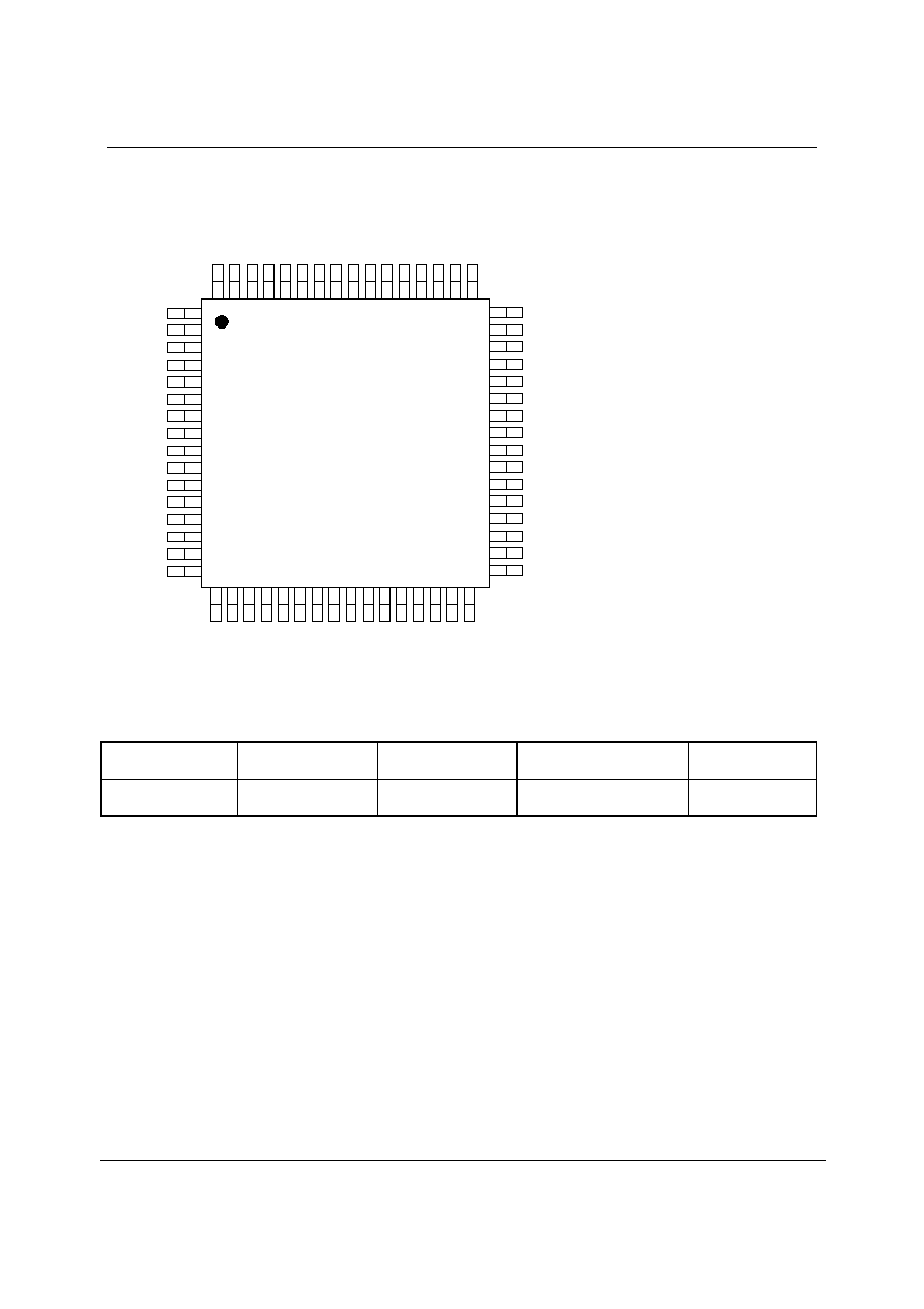
PIN CONFIGURATION
AV
DD
1
V
M
I
DAD
C
AG
ND
1
AU
X
1
L
AI
NO
P
R
AI
NV
G
L
AI
NV
G
R
RE
CL
RE
CR
AIN1L
AIN4L
AIN3R
AIN3L
AIN2R
AIN2L
AIN1R
AIN4R
AIN5L
AIN6L
R
ESET
B
BCL
K
MC
L
K
CL
DI
CE
DI
N2
DI
N3
DI
N4
D
ACL
RC
A
DCL
RC
VOUT4R
VOUT3L
VOUT3R
DACREFP2
VOUT4L
VOUT2L
GR2
VOUT2R
VMIDDAC
1
9
8
7
6
5
4
3
2
11
10
21 22 23 24 25 26 27
18 19 20
41
40
39
38
37
36
43
42
64 63 62 61 60 59 58
17
57 56 55 54
35
34
33
AI
NO
P
L
AIN5R
RE
F
ADC
Z
FLA
G1
Z
FLA
G2
DV
DD
DO
U
T
DI
N1
53 52 51 50 49
AU
X
3
L
AU
X
2
L
AUX
2
R
AUX
3
R
AU
X
1
R
DACREFP1
AVDD2
VOUT1L
VOUT1R
AIN6R
AIN7L
AIN7R
AIN8R
14
13
12
16
15
AIN8L
GR1
28 29 30 31 32
46
45
44
48
47
AGND2
DGND
ORDERING INFORMATION
DEVICE
TEMPERATURE
RANGE
PACKAGE
MOISTURE SENSITIVITY
LEVEL
PEAK SOLDERING
TEMPERATURE
WM8770SIFT/V -25
o
C to +85
o
C
64-lead TQFP
(Pb-free)
MSL3 260
o
C

WM8770
Production Data
w
PD Rev 4.1 June 2005
4
PIN DESCRIPTION
PIN NAME TYPE
DESCRIPTION
1 AIN1L
Analogue
Input
Channel 1 left input multiplexor virtual ground
2
AIN1R
Analogue Input
Channel 1 right input multiplexor virtual ground
3 AIN2L
Analogue
Input
Channel 2 left input multiplexor virtual ground
4 AIN2R
Analogue
Input
Channel 2 right input multiplexor virtual ground
5 AIN3L
Analogue
Input
Channel 3 left input multiplexor virtual ground
6 AIN3R
Analogue
Input
Channel 3 right input multiplexor virtual ground
7 AIN4L
Analogue
Input
Channel 4 left input multiplexor virtual ground
8 AIN4R
Analogue
Input
Channel 4 right input multiplexor virtual ground
9 AIN5L
Analogue
Input
Channel 5 left input multiplexor virtual ground
10 AIN5R
Analogue
Input
Channel 5 right input multiplexor virtual ground
11 AIN6L
Analogue
Input
Channel 6 left input multiplexor virtual ground
12 AIN6R
Analogue
Input
Channel 6 right input multiplexor virtual ground
13 AIN7L
Analogue
Input
Channel 7 left input multiplexor virtual ground
14 AIN7R
Analogue
Input
Channel 7 right input multiplexor virtual ground
15 AIN8L
Analogue
Input
Channel 8 left input multiplexor virtual ground
16 AIN8R
Analogue
Input
Channel 8 right input multiplexor virtual ground
17 AINOPL
Analogue
Output
Left channel multiplexor output
18 AINVGL
Analogue
Input
Left channel multiplexor virtual ground
19 AINVGR
Analogue
Input
Right channel multiplexor virtual ground
20 AINOPR
Analogue
Output
Right channel multiplexor output
21 RECL
Analogue
Output
Left channel input mux select output
22 RECR
Analogue
Output
Right channel input mux select output
23 REFADC
Analogue
Output
ADC reference buffer decoupling pin; 10uF external decoupling
24 VMIDADC
Analogue
Output
ADC midrail divider decoupling pin; 10uF external decoupling
25 AGND1 Supply
Analogue negative supply and substrate connection
26 AVDD1 Supply
Analogue positive supply
27 AUX1L
Analogue
input
3.1 Multiplexor channel 1 left virtual ground input
28 AUX1R
Analogue
input
3.1 Multiplexor channel 1 right virtual ground input
29 AUX2L
Analogue
input
3.1 Multiplexor channel 2 left virtual ground input
30 AUX2R
Analogue
input
3.1 Multiplexor channel 2 right virtual ground input
31 AUX3L
Analogue
input
3.1 Multiplexor channel 3 left virtual ground input
32 AUX3R
Analogue
input
3.1 Multiplexor channel 3 right virtual ground input
33 AVDD2 Supply
Analogue positive supply
34 VOUT1L
Analogue
output
DAC channel 1 left output
35 VOUT1R
Analogue
output
DAC channel 1 right output
36 DACREFP1 Supply
DAC positive reference supply
37 VOUT2L
Analogue
output
DAC channel 2 left output
38 GR1 Supply
DAC ground reference
39 VOUT2R
Analogue
output
DAC channel 2 right output
40 VMIDDAC
Analogue
output
DAC midrail decoupling pin ; 10uF external decoupling
41 VOUT3L
Analogue
output
DAC channel 3 left output
42 GR2 Supply
DAC ground reference
43 VOUT3R
Analogue
output
DAC channel 3 right output
44 DACREFP2 Supply
DAC positive reference supply
45 VOUT4L
Analogue
output
DAC channel 4 left output
46 VOUT4R
Analogue
output
DAC channel 4 right output
47 AGND2 Supply
Analogue negative supply and substrate connection
48 DGND Supply
Digital negative supply
49 DVDD Supply
Digital positive supply
50 ZFLAG1
Digital
output
DAC Zero Flag output
51 ZFLAG2
Digital
output
DAC Zero Flag output

Production Data
WM8770
w
PD Rev 4.1 June 2005
5
PIN NAME TYPE
DESCRIPTION
52 DOUT
Digital
output
ADC data output
53 DIN1
Digital
Input
DAC channel 1 data input
54 DIN2
Digital
Input
DAC channel 2 data input
55 DIN3
Digital
Input
DAC channel 3 data input
56 DIN4
Digital
Input
DAC channel 4 data input
57 DACLRC
Digital
input/output
DAC left/right word clock
58 ADCLRC
Digital
input/output
ADC left/right word clock
59 BCLK
Digital
input/output
ADC and DAC audio interface bit clock
60 MCLK
Digital
input
Master DAC and ADC clock; 256, 384, 512 or 768fs (fs = word clock
frequency)
61 CL
Digital
input
Serial interface clock (5V tolerant)
62 DI
Digital
input
Serial interface data (5V tolerant)
63 CE
Digital
input
Serial interface Latch signal (5V tolerant)
64 RESETB
Digital
input
Device reset input (mutes DAC outputs, resets gain stages to 0dB)
(5V tolerant)
Note: Digital input pins have Schmitt trigger input buffers and are 5V tolerant.

WM8770
Production Data
w
PD Rev 4.1 June 2005
6
ABSOLUTE MAXIMUM RATINGS
Absolute Maximum Ratings are stress ratings only. Permanent damage to the device may be caused by continuously operating at
or beyond these limits. Device functional operating limits and guaranteed performance specifications are given under Electrical
Characteristics at the test conditions specified.
ESD Sensitive Device. This device is manufactured on a CMOS process. It is therefore generically susceptible
to damage from excessive static voltages. Proper ESD precautions must be taken during handling and storage
of this device.
Wolfson tests its package types according to IPC/JEDEC J-STD-020B for Moisture Sensitivity to determine acceptable storage
conditions prior to surface mount assembly. These levels are:
MSL1 = unlimited floor life at <30
∞
C / 85% Relative Humidity. Not normally stored in moisture barrier bag.
MSL2 = out of bag storage for 1 year at <30
∞
C / 60% Relative Humidity. Supplied in moisture barrier bag.
MSL3 = out of bag storage for 168 hours at <30
∞
C / 60% Relative Humidity. Supplied in moisture barrier bag.
The Moisture Sensitivity Level for each package type is specified in Ordering Information.
CONDITION
MIN MAX
Digital supply voltage
-0.3V +3.63V
Analogue supply voltage
-0.3V +7V
Voltage range digital inputs (DI, CL, CE & RESETB)
DGND -0.3V
+7V
Voltage range digital inputs (MCLK, DIN[3:0], ADCLRC, DACLRC &
BCLK)
DGND -0.3V
DVDD + 0.3V
Voltage range analogue inputs
AGND -0.3V
AVDD +0.3V
Master Clock Frequency
37MHz
Operating temperature range, T
A
-25
∞
C +85
∞
C
Storage temperature
-65
∞
C +150
∞
C
Note:
1.
Analogue and digital grounds must always be within 0.3V of each other.
RECOMMENDED OPERATING CONDITIONS
PARAMETER SYMBOL
TEST
CONDITIONS
MIN
TYP
MAX
UNIT
Digital supply range
DVDD
2.7
3.6
V
Analogue supply range
AVDD
2.7
5.5
V
Ground
AGND,
DGND
0 V
Difference DGND to AGND
-0.3
0
+0.3
V
Note: digital supply DVDD must never be more than 0.3V greater than AVDD.
Production Data
WM8770
w
PD Rev 4.1 June 2005
7
ELECTRICAL CHARACTERISTICS
Test Conditions
AVDD = 5V, DVDD = 3.3V, AGND = 0V, DGND = 0V, T
A
= +25
o
C, fs = 48kHz, MCLK = 256fs, ADC/DAC in Slave Mode unless
otherwise stated.
PARAMETER SYMBOL
TEST
CONDITIONS
MIN
TYP
MAX
UNIT
Digital Logic Levels (TTL Levels)
Input LOW level
V
IL
0.8
V
Input HIGH level
V
IH
2.0
V
Output LOW
V
OL
I
OL
=1mA
0.1
x
DVDD
V
Output HIGH
V
OH
I
OH
-1mA
0.9 x DVDD
V
Analogue Reference Levels
Reference voltage
V
VMID
AVDD/2
V
Potential divider resistance
R
VMID
AVDD to VMID and
VMID to AGND
50k
DAC Performance (Load
= 10k, 50pF)
0dBFs Full scale output voltage
1.0
x
AVDD/5
Vrms
SNR (Note 1,2)
A-weighted,
@ fs = 48kHz
100 106
dB
SNR (Note 1,2)
A-weighted
@ fs = 96kHz
106
dB
Dynamic Range (Note 2)
DNR
A-weighted, -60dB
full scale input
100 106
dB
Total Harmonic Distortion (THD)
1kHz, 0dBFs
-94
-88
dB
DAC channel separation
110
dB
DAC analogue Volume Gain
Step Size
1
dB
DAC analogue Volume Gain
Range
1kHz Input
0 to -100
dB
Output Noise
A-weighted output
muted
-116 dB
DAC analogue Volume Mute
Attenuation
1kHz Input, 0dB gain
100
dB
1kHz 100mVpp
50
dB
Power Supply Rejection Ratio
PSRR
20Hz to 20kHz
100mVpp
45 dB
ADC Performance
Input Signal Level (0dB)
1.0
x
AVDD/5
Vrms
SNR (Note 1,2)
A-weighted, 0dB gain
@ fs = 48kHz
102
dB
SNR (Note 1,2)
A-weighted, 0dB gain
@ fs = 96kHz
96
dB
Dynamic Range (note 2)
A-weighted, -60dB
full scale input
102 dB
kHz, 0dBFs
-89
dB
Total Harmonic Distortion (THD)
1kHz, -1dBFs
-94
-90
dB
ADC Channel Separation
1kHz Input
85
dB
Programmable Gain Step Size
1.0 dB
Programmable Gain Range
1kHz Input
-12 to +19
dB
Mute Attenuation
1kHz Input, 0dB gain
82
dB
1kHz 100mVpp
50
dB
Power Supply Rejection Ratio
PSRR
20Hz to 20kHz
100mVpp
45 dB
WM8770
Production Data
w
PD Rev 4.1 June 2005
8
Test Conditions
AVDD = 5V, DVDD = 3.3V, AGND = 0V, DGND = 0V, T
A
= +25
o
C, fs = 48kHz, MCLK = 256fs, ADC/DAC in Slave Mode unless
otherwise stated.
PARAMETER SYMBOL
TEST
CONDITIONS
MIN
TYP
MAX
UNIT
Analogue input (AIN) to Analogue output (VOUT) (Load=10k, 50pF, gain = 0dB) Bypass Mode
0dB Full scale output voltage
1.0 x
AVDD/5
Vrms
SNR (Note 1)
104
dB
1kHz, 0dB
-90
dB
THD
1kHz, -3dB
-95
dB
1kHz
100mVpp
50 dB
Power Supply Rejection Ratio
PSRR
20Hz to 20kHz
100mVpp
45 dB
Mute Attenuation
1kHz,
0dB
100
dB
Supply Current
Analogue supply current
AVDD = 5V
120
mA
Digital supply current
DVDD
=
3.3V
16
mA
Notes:
1.
Ratio of output level with 1kHz full scale input, to the output level with all zeros into the digital input, measured `A'
weighted.
2.
All performance measurements done with 20kHz low pass filter, and where noted an A-weight filter. Failure to use
such a filter will result in higher THD+N and lower SNR and Dynamic Range readings than are found in the Electrical
Characteristics. The low pass filter removes out of band noise; although it is not audible it may affect dynamic
specification values.
3.
VMID decoupled with 10uF and 0.1uF capacitors (smaller values may result in reduced performance).
TERMINOLOGY
1.
Signal-to-noise ratio (dB) - SNR is a measure of the difference in level between the full scale output and the output
with no signal applied. (No Auto-zero or Automute function is employed in achieving these results).
2.
Dynamic range (dB) - DNR is a measure of the difference between the highest and lowest portions of a signal.
Normally a THD+N measurement at 60dB below full scale. The measured signal is then corrected by adding the 60dB
to it. (e.g. THD+N @ -60dB= -32dB, DR= 92dB).
3.
THD+N (dB) - THD+N is a ratio, of the rms values, of (Noise + Distortion)/Signal.
4.
Stop band attenuation (dB) - Is the degree to which the frequency spectrum is attenuated (outside audio band).
5.
Channel Separation (dB) - Also known as Cross-Talk. This is a measure of the amount one channel is isolated from
the other. Normally measured by sending a full scale signal down one channel and measuring the other.
6.
Pass-Band Ripple - Any variation of the frequency response in the pass-band region.

Production Data
WM8770
w
PD Rev 4.1 June 2005
9
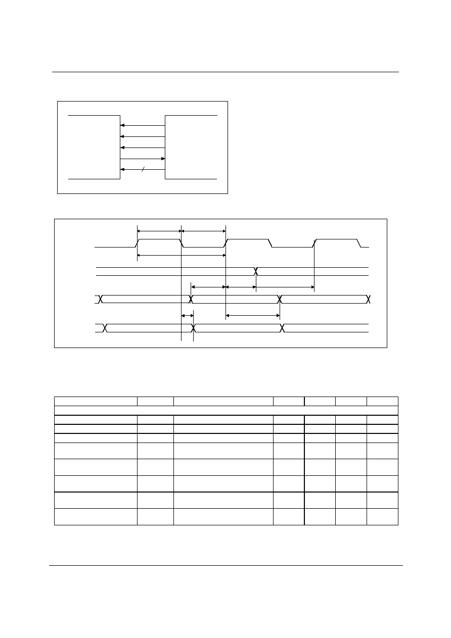
MASTER CLOCK TIMING
MCLK
t
MCLKL
t
MCLKH
t
MCLKY
Figure 1 Master Clock Timing Requirements
Test Conditions
AVDD = 5V, DVDD = 3.3V, AGND = 0V, DGND = 0V, T
A
= +25
o
C, fs = 48kHz, MCLK = 256fs, ADC/DAC in Slave Mode unless
otherwise stated.
PARAMETER SYMBOL
TEST
CONDITIONS
MIN
TYP
MAX
UNIT
System Clock Timing Information
MCLK System clock pulse width high
t
MCLKH
11
ns
MCLK System clock pulse width low
t
MCLKL
11
ns
MCLK System clock cycle time
t
MCLKY
28
1000
ns
MCLK Duty cycle
40:60
60:40
Power-saving mode activated
After
MCLK
stopped
2 10
µs
Normal mode resumed
After
MCLK
re-started
0.5 1
MCLK
cycle
Table 1 Master Clock Timing Requirements
Note: If MCLK period is longer than maximum specified above, DACs are powered down with internal digital audio filters
being reset. In this mode, all registers will retain their values and can be accessed in the normal manner through the
control interface. Once MCLK is restored, the DACs are automatically powered up.
DIGITAL AUDIO INTERFACE ≠ MASTER MODE
Figure 2 Audio Interface - Master Mode
BCLK
DOUT
ADCLRC
DIN1/2/3/4
DACLRC
WM8770
CODEC
DSP/
ENCODER/
DECODER
4

WM8770
Production Data
w
PD Rev 4.1 June 2005
10
BCLK
(Output)
DOUT
ADCLRC/
DACLRC
(Outputs)
t
DL
DIN1/2/3/4
t
DDA
t
DHT
t
DST
Figure 3 Digital Audio Data Timing ≠ Master Mode
Test Conditions
AVDD = 5V, DVDD = 3.3V, AGND = 0V, DGND = 0V, T
A
= +25
o
C, fs = 48kHz, MCLK = 256fs, ADC/DAC in Slave Mode unless
otherwise stated.
PARAMETER SYMBOL
TEST
CONDITIONS
MIN
TYP
MAX
UNIT
Audio Data Input Timing Information
ADCLRC/DACLRC
propagation delay from
BCLK falling edge
t
DL
0
10
ns
DOUT propagation delay
from BCLK falling edge
t
DDA
0
10
ns
DIN1/2/3/4 setup time to
BCLCK rising edge
t
DST
10
ns
DIN1/2/3/4 hold time from
BCLK rising edge
t
DHT
10
ns
Table 2 Digital Audio Data Timing ≠ Master Mode
Production Data
WM8770
w
PD Rev 4.1 June 2005
11
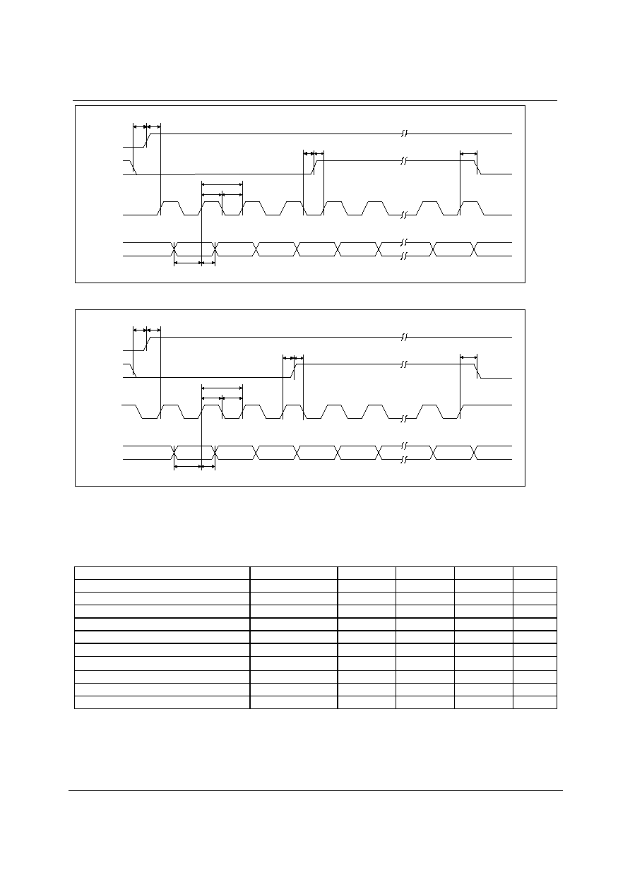
DIGITAL AUDIO INTERFACE ≠ SLAVE MODE
Figure 4 Audio Interface ≠ Slave Mode
BCLK
DACLRC/
ADCLRC
t
BCH
t
BCL
t
BCY
DIN1/2/3/4
DOUT
t
LRSU
t
DS
t
LRH
t
DH
t
DD
Figure 5 Digital Audio Data Timing ≠ Slave Mode
Test Conditions
AVDD = 5V, DVDD = 3.3V, AGND = 0V, DGND = 0V, T
A
= +25
o
C, fs = 48kHz, MCLK = 256fs, ADC/DAC in Slave Mode unless
otherwise stated.
PARAMETER SYMBOL
TEST
CONDITIONS
MIN
TYP
MAX
UNIT
Audio Data Input Timing Information
BCLK cycle time
t
BCY
50
ns
BCLK pulse width high
t
BCH
20
ns
BCLK pulse width low
t
BCL
20
ns
DACLRC/ADCLRC set-up
time to BCLK rising edge
t
LRSU
10
ns
DACLRC/ADCLRC hold
time from BCLK rising edge
t
LRH
10
ns
DIN1/2/3/4 set-up time to
BCLK rising edge
t
DS
10
ns
DIN1/2/3/4 hold time from
BCLK rising edge
t
DH
10
ns
DOUT propagation delay
from BCLK falling edge
t
DD
0
10
ns
Table 3 Digital Audio Data Timing ≠ Slave Mode
Note: ADCLRC and DACLRC should be synchronous with MCLK, although the WM8770 interface is tolerant of phase
variations or jitter on these signals.
BCLK
DOUT
ADCLRC
DIN1/2/3/4
DACLRC
WM8770
CODEC
DSP
ENCODER/
DECODER
4

WM8770
Production Data
w
PD Rev 4.1 June 2005
12
MPU INTERFACE TIMING
t
RCHO
t
RCSU
CE
CL
DI
t
CSL
t
DHO
t
DSU
t
CSH
t
SCY
t
SCH
t
SCL
t
SCS
LSB
t
CSS
RESETB
Figure 6 SPI Compatible Control Interface Input Timing
Test Conditions
AVDD = 5V, DVDD = 3.3V, AGND = 0V, DGND = 0V, T
A
= +25
o
C, fs = 48kHz, MCLK = 256fs, ADC/DAC in Slave Mode unless
otherwise stated.
PARAMETER SYMBOL
MIN
TYP
MAX
UNIT
CE to RESETB hold time
t
RCSU
20
ns
RESETB to CL setup time
t
RCHO
20
ns
CL rising edge to CE rising edge
t
SCS
60
ns
CL pulse cycle time
t
SCY
80
ns
CL pulse width low
t
SCL
30
ns
CL pulse width high
t
SCH
30
ns
DI to CL set-up time
t
DSU
20
ns
CL to DI hold time
t
DHO
20
ns
CE pulse width low
t
CSL
20
ns
CE pulse width high
t
CSH
20
ns
CE rising to CL rising
t
CSS
20
ns
Table 4 3 Wire SPI Compatible Control Interface Input Timing Information
Production Data
WM8770
w
PD Rev 4.1 June 2005
13
CE
CL
DI
t
SCY
t
SCH
t
SCL
t
DSU
t
DHO
t
CS
t
CP
A7
t
CH
D15
t
RCES
t
RCLH
RESETB
Figure 7 3 Wire CCB Compatible Interface Input Timing Information ≠ CL Stopped Low
CE
CL
DI
t
SCY
t
SCH
t
SCL
t
DSU
t
DHO
t
CS
t
CP
A7
t
CH
D15
t
RCES
t
RCLH
RESETB
Figure 8 3 Wire CCB Compatible Interface Input Timing Information ≠ CL Stopped High
Test Conditions
AVDD = 5V, DVDD = 3.3V, AGND = 0V, DGND = 0V, T
A
= +25
o
C, fs = 48kHz, MCLK = 256fs, ADC/DAC in Slave Mode unless
otherwise stated.
PARAMETER SYMBOL
MIN
TYP
MAX
UNIT
CE to RESETB setup time
t
RCES
20
ns
RESETB to CL hold time
t
RCLH
20
ns
DI to CL setup time
t
DSU
20
ns
CL to DI hold time
t
DHO
20
ns
CL to CE setup time
t
CS
20
ns
CE to CL wait time
t
CP
20
ns
CL to CE hold time
t
CH
20
ns
CL pulse width high
t
SCH
30
ns
CL pulse width low
t
SCL
30
ns
CL pulse cycle time
t
SCY
80
ns
Table 5 3 wire CCB Compatible Interface Input Timing Information
WM8770
Production Data
w
PD Rev 4.1 June 2005
14
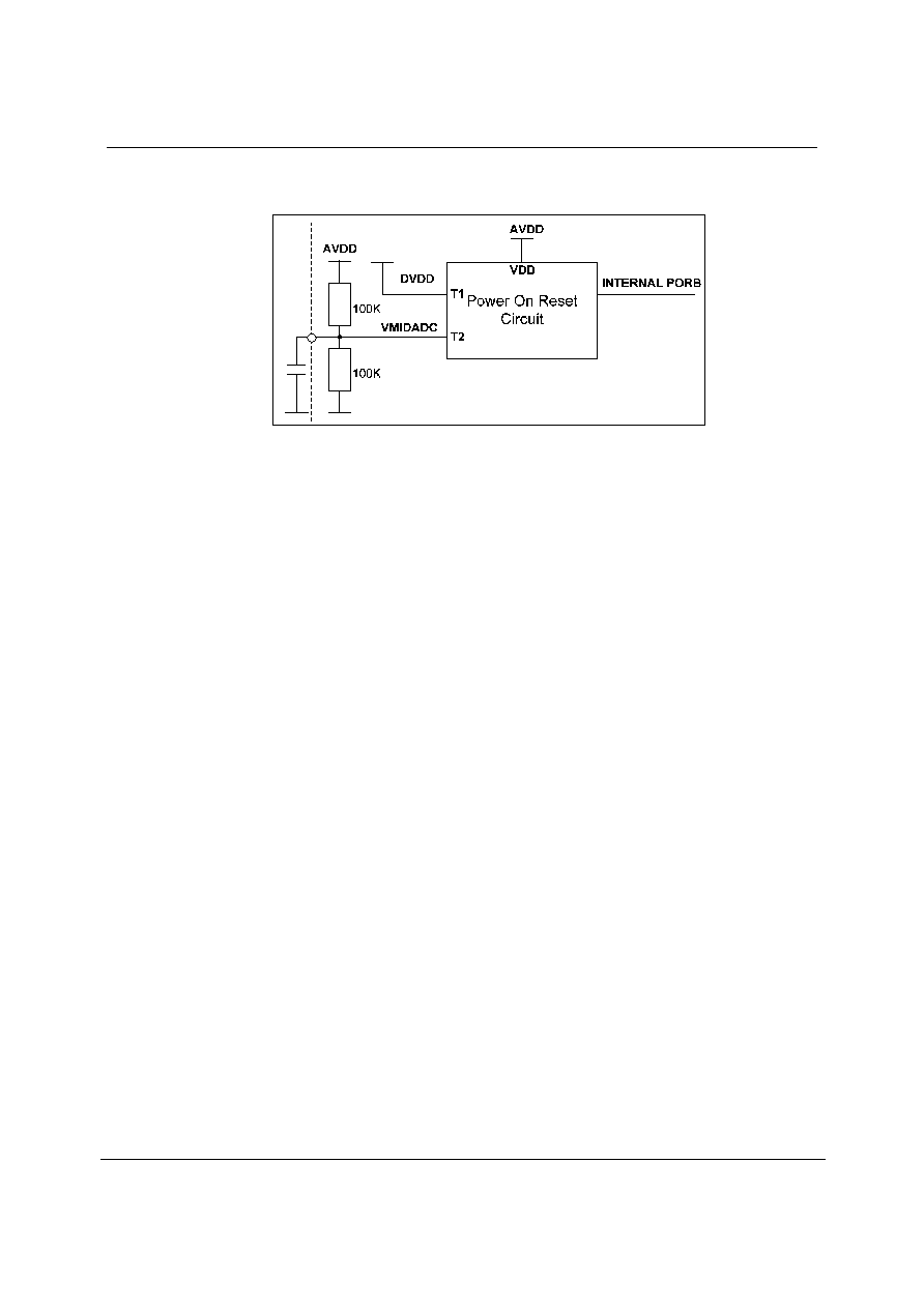
INTERNAL POWER ON RESET CIRCUIT
Figure 9 Internal Power On Reset Circuit Schematic
The WM8770 includes an internal Power On Reset Circuit which is used to reset the digital logic into
a default state after power up.
Figure 9 shows a schematic of the internal POR circuit. The POR circuit is powered from AVDD. The
circuit monitors DVDD and VMIDADC and asserts PORB low if DVDD or VMIDADC are below the
minimum threshold Vpor_off.
On power up, the POR circuit requires AVDD to be present to operate. PORB is asserted low until
AVDD, DVDD and VMIDADC are established. When AVDD, DVDD, and VMIDADC have been
established, PORB is released high, all registers are in their default state and writes to the digital
interface may take place.
On power down, PORB is asserted low whenever DVDD or VMIDADC drop below the minimum
threshold Vpor_off.
If AVDD is removed at any time, the internal Power On Reset circuit is powered down and PORB will
follow AVDD.
In most applications the time required for the device to release PORB high will be determined by the
charge time of the VMIDADC node.
Production Data
WM8770
w
PD Rev 4.1 June 2005
15
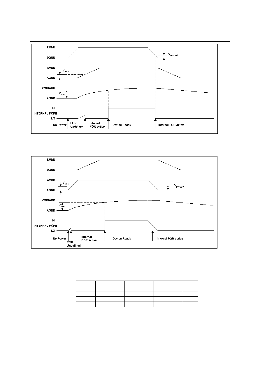
Figure 10 Typical Power up sequence where DVDD is powered before AVDD.
Figure 11 Typical Power up sequence where AVDD is powered before DVDD
Typical POR Operation (typical values, not tested)
SYMBOL MIN
TYP
MAX UNIT
V
pora
0.5 0.7 1.0
V
V
porr
0.5 0.7 1.1
V
V
pora_off
1.0
1.4
2.0 V
V
pord_off
0.6
0.8
1.0 V

WM8770
Production Data
w
PD Rev 4.1 June 2005
16
In a real application the designer is unlikely to have control of the relative power up sequence of
AVDD and DVDD. Using the POR circuit to monitor VMIDADC ensures a reasonable delay between
applying power to the device and Device Ready.
Figure 10 and Figure 11 show typical power up scenarios in a real system. Both AVDD and DVDD
must be established and VMIDADC must have reached the threshold Vporr before the device is
ready and can be written to. Any writes to the device before Device Ready will be ignored.
Figure 10 shows DVDD powering up before AVDD. Figure 11 shows AVDD powering up before
DVDD. In both cases, the time from applying power to Device Ready is dominated by the charge
time of VMIDADC.
A 10uF cap is recommended for decoupling on VMIDADC. The charge time for VMIDADC will
dominate the time required for the device to become ready after power is applied. The time required
for VMIDADC to reach the threshold is a function of the VMIDADC resistor string and the decoupling
capacitor. The Resistor string has a typical equivalent resistance of 50kohm (+/-20%). Assuming a
10uF capacitor, the time required for VMIDADC to reach threshold of 1V is approx 110ms.

Production Data
WM8770
w
PD Rev 4.1 June 2005
17
DEVICE DESCRIPTION
INTRODUCTION
WM8770 is a complete 8-channel DAC, 2-channel ADC audio codec, including digital interpolation
and decimation filters, multi-bit sigma delta stereo ADC, and switched capacitor multi-bit sigma delta
DACs with analogue volume controls on each channel and output smoothing filters.
The device is implemented as four separate stereo DACs and a stereo ADC with flexible input
multiplexor, in a single package and controlled by a single interface.
The four stereo channels may either be used to implement a 5.1 channel surround system, with
additional stereo channel for a stereo mix down channel, or for a complete 7.1 channel surround
system.
An analogue bypass path option is available, to allow stereo analogue signals from any of the 8
stereo inputs to be sent to the stereo outputs via the main volume controls. This allows a purely
analogue input to analogue output high quality signal path to be implemented if required. This would
allow, for example, the user to play back a 5.1 channel surround movie through 6 of the DACs, whilst
playing back a separate analogue or digital signal into a remote room installation.
Each stereo DAC has its own data input DIN1/2/3/4. DAC word clock DACLRC is shared between
them. The stereo ADC has it's own data output DOUT, and word clock ADCLRC. BITCLK and MCLK
are shared between the ADCs and DACs. The Audio Interface may be configured to operate in either
master or slave mode. In Slave mode ADCLRC, DACLRC and BCLK are all inputs. In Master mode
ADCLRC, DACLRC and BCLK are all outputs.
The input multiplexor to the ADC is configured to allow large signal levels to be input to the ADC,
using external resistors to reduce the amplitude of larger signals to within the normal operating range
of the ADC. The ADC input PGA also allows input signals to be gained up to +19dB and attenuated
down to -12dB. This allows the user maximum flexibility in the use of the ADC.
A selectable stereo record output is also provided on RECL/R. It is intended that the RECL/R outputs
are only used to drive a high impedance buffer.
Each DAC has its own analogue and separate digital volume control. The analogue volume control is
adjustable in 1dB steps and the digital volume control in 0.5dB steps. The analogue and digital
volume controls may be operated independently. In addition a zero cross detect circuit is provided for
each DAC for both analogue and digital volume controls. When analogue volume zero-cross
detection is enabled the attenuation values are only updated when the input signal to the gain stage
is close to the analogue ground level. The digital volume control detects a transition through the zero
point before updating the volume. This minimises audible clicks and `zipper' noise as the gain values
change.
Additionally, 6 of the DAC outputs incorporate an input selector and mixer allowing an external 6
channel, or 5.1 channel signal, to be either switched into the signal path in place of the DAC signal or
mixed with the DAC signal before the volume controls. This allows the device to be used as a 6
channel volume control for an externally provided 5.1 type analogue input. Use of external resistors
allows larger input levels to be accepted by the device, giving maximum user flexibility.
Control of internal functionality of the device is by 3-wire serial control interface. An SPI or CCB type
interface may used, selectable by the state of the CE pin on the rising edge of RESETB. The control
interface may be asynchronous to the audio data interface as control data will be re-synchronised to
the audio processing internally.
CE, CL, DI and RESETB are 5V tolerant with TTL input thresholds, allowing the WM8770 to used
with DVDD = 3.3V and be controlled by a controller with 5V output.
Operation using system clock of 128fs, 192fs, 256fs, 384fs, 512fs or 768fs is provided. In Slave
mode selection between clock rates is automatically controlled. In master mode the master clock to
sample rate ratio is set by control bits ADCRATE and DACRATE. ADC and DAC may run at different
rates within the constraint of a common master clock for the ADC and DACs. For example with
master clock at 24.576MHz, a DAC sample rate of 96kHz (256fs mode) and an ADC sample rate of
48kHz (512fs mode) can be accomadated. Master clock.Sample rates (fs) from less than 8ks/s up to
192ks/s are allowed, provided the appropriate system clock is input.
The audio data interface supports right, left and I
2
S interface formats along with a highly flexible DSP
serial port interface.

WM8770
Production Data
w
PD Rev 4.1 June 2005
18
AUDIO DATA SAMPLING RATES
In a typical digital audio system there is only one central clock source producing a reference clock to
which all audio data processing is synchronised. This clock is often referred to as the audio system's
Master Clock. The external master system clock can be applied directly through the MCLK input pin
with no software configuration necessary. In a system where there are a number of possible sources
for the reference clock it is recommended that the clock source with the lowest jitter be used to
optimise the performance of the ADC and DAC.
The master clock for WM8770 supports DAC and ADC audio sampling rates from 256fs to 768fs,
where fs is the audio sampling frequency (DACLRC or ADCLRC) typically 32kHz, 44.1kHz, 48kHz or
96kHz (the DAC also supports operation at 128fs and 192fs and 192kHz sample rate). The master
clock is used to operate the digital filters and the noise shaping circuits.
In Slave mode the WM8770 has a master detection circuit that automatically determines the
relationship between the master clock frequency and the sampling rate (to within +/- 32 system
clocks). If there is a greater than 32 clocks error the interface is disabled and maintains the output
level at the last sample. The master clock must be synchronised with ADCLRC/DACLRC, although
the WM8770 is tolerant of phase variations or jitter on this clock. Table 6 shows the typical master
clock frequency inputs for the WM8770.
The signal processing for the WM8770 typically operates at an oversampling rate of 128fs for both
ADC and DAC. The exception to this for the DAC is for operation with a 128/192fs system clock, e.g.
for 192KHz operation where the oversampling rate is 64fs. For ADC operation at 96kHz it is
recommended that the user set the ADCOSR bit. This changes the ADC signal processing
oversample rate to 64fs.
System Clock Frequency (MHz)
128fs 192fs
SAMPLING
RATE
(DACLRC/
ADCLRC)
DAC ONLY
256fs 384fs 512fs 768fs
32kHz 4.096 6.144 8.192 12.288
16.384
24.576
44.1kHz 5.6448 8.467 11.2896
16.9340
22.5792 33.8688
48kHz 6.144 9.216 12.288
18.432
24.576
36.864
96kHz 12.288
18.432 24.576 36.864
Unavailable
Unavailable
192kHz 24.576 36.864
Unavailable
Unavailable
Unavailable
Unavailable
Table 6 System Clock Frequencies Versus Sampling Rate
In Master mode BCLK, DACLRC and ADCLRC are generated by the WM8770. The frequencies of
ADCLRC and DACLRC are set by setting the required ratio of MCLK to DACLRC and ADCLRC using
the DACRATE and ADCRATE control bits (Table 7).
ADCRATE[2:0]/
DACRATE[2:0]
MCLK:ADCLRC/DACLRC
RATIO
000
128fs (DAC Only)
001
192fs (DAC Only)
010 256fs
011 384fs
100 512fs
101 768fs
Table 7 Master Mode MCLK: ADCLRC/DACLRC Ratio Select
Production Data
WM8770
w
PD Rev 4.1 June 2005
19
Table 8 shows the settings for ADCRATE and DACRATE for common sample rates and MCLK
frequencies.
System Clock Frequency (MHz)
128fs 192fs 256fs 384fs 512fs 768fs
SAMPLING
RATE
(DACLRC/
ADCLRC)
DACRATE
=000
DACRATE
=001
ADCRATE/
DACRATE
=010
ADCRATE/
DACRATE
=011
ADCRATE/
DACRATE
=100
ADCRATE/
DACRATE
=101
32kHz 4.096 6.144 8.192 12.288
16.384
24.576
44.1kHz 5.6448 8.467 11.2896 16.9340 22.5792 33.8688
48kHz 6.144 9.216 12.288 18.432 24.576 36.864
96kHz 12.288 18.432 24.576 36.864
Unavailable
Unavailable
192kHz
24.576
36.864
Unavailable Unavailable Unavailable Unavailable
Table 8 Master Mode ADC/DACLRC Frequency Selection
BCLK is also generated by the WM8770. The frequency of BCLK depends on the mode of operation.
In 128/192fs modes (DACRATE=000 or 001) BCLK = MCLK/2. In 256/384/512fs modes
(ADCRATE/DACRATE=010 or 011 or 100) BCLK = MCLK/4. However if DSP mode is selected as
the audio interface mode then BCLK=MCLK. This is to ensure that there are sufficient BCLKs to
clock in all eight channels. Note that DSP mode cannot be used in 128fs mode for word lengths
greater than 16 bits or in 192fs mode for word lengths greater than 24 bits.
ZERO DETECT
The WM8770 has a zero detect circuit for each DAC channel which detects when 1024 consecutive
zero samples have been input. Two zero flag outputs (ZFLAG1 and ZFLAG2) may be programmed to
output the zero detect signals (see Table 9) which may then be used to control external muting
circuits. A `1' on ZFLAG1 or ZFLAG2 indicates a zero detect. When a DAC is powered down
ZFLAG1 and ZFLAG2 will go high by default if the Zero Detect is selected for that DAC. When this
DAC is powered off, the Bypass path is selected and there is an external mute circuit controlled by
ZFLAG1 or ZFLAG2, the Zero Detect feature should be de-selected or the output will be muted.
The zero detect may also be used to automatically enable the PGA mute by setting IZD. The zero
flag output may be disabled by setting DZFM to 0000. The zero flag signal for a DAC channel will
only be enabled if that channel is enabled as an input to the output summing stage.
DZFM[3:0] ZFLAG1
ZFLAG2
0000
Zero flag disabled
Zero flag disabled
0001
All channels zero
All channels zero
0010
Left channels zero
Right channels zero
0011
Channel 1 zero
Channels 2-4 zero
0100
Channel 1 zero
Channel 2 zero
0101
Channel 1 zero
Channel 3 zero
0110
Channel 1 zero
Channel 4 zero
0111
Channel 2 zero
Channel 3 zero
1000
Channel 2 zero
Channel 4 zero
1001
Channel 3 zero
Channel 4 zero
1010
Channels 1-3 zero
Channel 4 zero
1011
Channel 1 zero
Channels 2 & 3 zero
1100
Channel 1 left zero
Channel 1 right zero
1101
Channel 2 left zero
Channel 2 right zero
1110
Channel 3 left zero
Channel 3 right zero
1111
Channel 4 left zero
Channel 4 right zero
Table 9 Zero Flag Output Select
WM8770
Production Data
w
PD Rev 4.1 June 2005
20
POWERDOWN MODES
The WM8770 has powerdown control bits allowing specific parts of the WM8770 to be powered off
when not being used. The 8-channel input source selector and input buffer may be powered down
using control bit AINPD. When AINPD is set all inputs to the source selector (AIN1l/R to AIN8L/R)
are switched to a buffered VMIDADC. Control bit ADCPD powers off the ADC and also the ADC input
PGAs.The four stereo DACs each have a separate powerdown control bit, DACPD[3:0] allowing
individual steteo DACs to be powered off when not in use. The analogue output mixers and EVRs
may also be powered down by setting OUTPD[3:0]. OUTPD[3:0] also switches the analogue outputs
VOUTL/R to VMIDDAC to maintain a dc level on the output. Setting AINPD, ADCPD, DACPD[3:0]
and OUTPD[3:0] will powerdown everything except the references VMIDADC, ADCREF and
VMIDDAC. These may be powered down by setting PDWN. Setting PDWN will override all other
powerdown control bits. It is recommended that the 8-channel input mux and buffer, ADC, DAC and
output mixers and EVRs are powered down before setting PDWN. The default is for all powerdown
bits to be set except PDWN.
The Powerdown control bits allow parts of the device to be powered down when not in use. For
example, if only an analogue bypass path from AINL/R to VOUTL/R is required the ADCPD and
DACPD[3:0] control bits may be set leaving the analogue input and analogue output powered up.
DIGITAL AUDIO INTERFACE
MASTER AND SLAVE MODES
The audio interface operates in either Slave or Master mode, selectable using the MS control bit. In
both Master and Slave modes DACDAT is always an input to the WM8770 and ADCDAT is always
an output. The default is Slave mode.
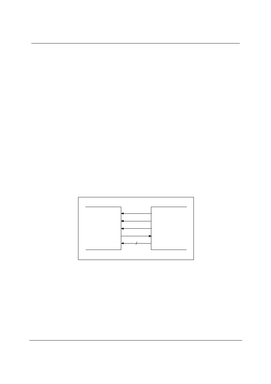
In Slave mode (MS=0) ADCLRC, DACLRC and BCLK are inputs to the WM8770 (Figure 12).
DIN1/2/3/4, ADCLRC and DACLRC are sampled by the WM8770 on the rising edge of BCLK. ADC
data is output on DOUT and changes on the falling edge of BCLK. By setting control bit BCLKINV the
polarity of BCLK may be reversed so that DIN1/2/3/4, ADCLRC and DACLRC are sampled on the
falling edge of BCLK and DOUT changes on the rising edge of BCLK.
Figure 12 Slave Mode
BCLK
DOUT
ADCLRC
DIN1/2/3/4
DACLRC
WM8770
CODEC
DSP
ENCODER/
DECODER
4
Production Data
WM8770
w
PD Rev 4.1 June 2005
21
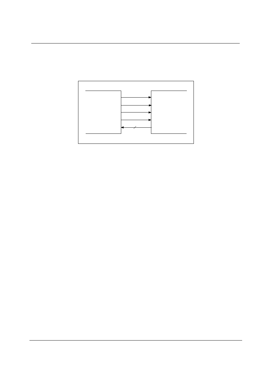
In Master mode (MS=1) ADCLRC, DACLRC and BCLK are outputs from the WM8770 (Figure 13).
ADCLRC, DACLRC and BITCLK are generated by the WM8770. DIN1/2/3/4 are sampled by the
WM8770 on the rising edge of BCLK so the controller must output DAC data that changes on the
falling edge of BCLK. ADCDAT is output on DOUT and changes on the falling edge of BCLK. By
setting control bit BCLKINV the polarity of BCLK may be reversed so that DIN1/2/3/4 are sampled on
the falling edge of BCLK and DOUT changes on the rising edge of BCLK.
Figure 13 Master Mode
AUDIO INTERFACE FORMATS
Audio data is applied to the internal DAC filters, or output from the ADC filters, via the Digital Audio
Interface. 5 popular interface formats are supported:
∑
Left Justified mode
∑
Right Justified mode
∑
I
2
S mode
∑
DSP
Early
mode
∑
DSP Late mode
All 5 formats send the MSB first and support word lengths of 16, 20, 24 and 32 bits, with the
exception of 32 bit right justified mode, which is not supported.
In left justified, right justified and I
2
S modes, the digital audio interface receives DAC data on the
DIN1/2/3/4 inputs and outputs ADC data on DOUT. Audio Data for each stereo channel is time
multiplexed with ADCLRC/DACLRC indicating whether the left or right channel is present.
ADCLRC/DACLRC is also used as a timing reference to indicate the beginning or end of the data
words.
In left justified, right justified and I
2
S modes, the minimum number of BCLKs per DACLRC/ADCLRC
period is 2 times the selected word length. ADCLRC/DACLRC must be high for a minimum of word
length BCLKs and low for a minimum of word length BCLKs. Any mark to space ratio on
ADCLRC/DACLRC is acceptable provided the above requirements are met.
In DSP early or DSP late mode, all 8 DAC channels are time multiplexed onto DIN1. DACLRC is
used as a frame sync signal to identify the MSB of the first word. The minimum number of BCLKs
per DACLRC period is 8 times the selected word length. Any mark to space ratio is acceptable on
DACLRC provided the rising edge is correctly positioned. The ADC data may also be output in DSP
early or late modes, with ADCLRC used as a frame sync to identify the MSB of the first word. The
minimum number of BCLKs per ADCLRC period is 2 times the selected word length
BCLK
DOUT
ADCLRC
DIN1/2/3/4
DACLRC
WM8770
CODEC
DSP/
ENCODER/
DECODER
4
WM8770
Production Data
w
PD Rev 4.1 June 2005
22
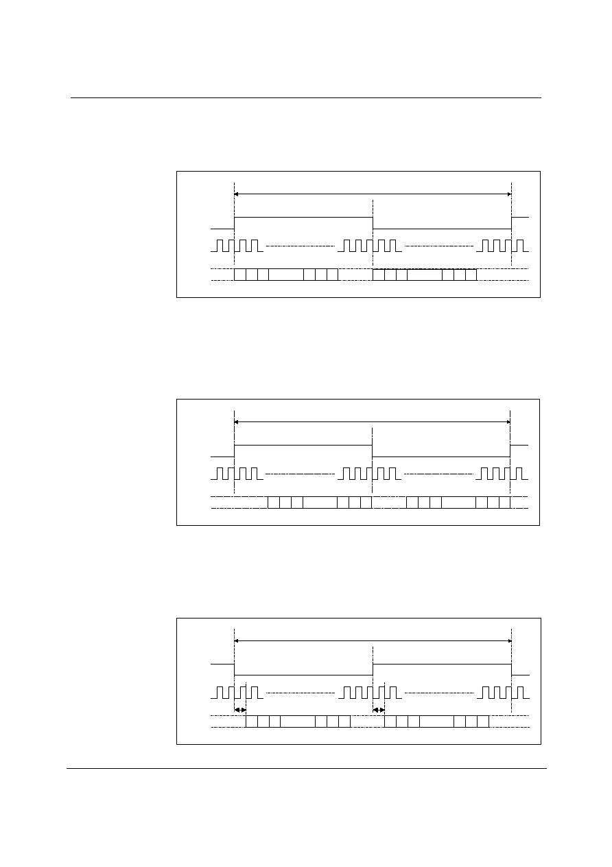
LEFT JUSTIFIED MODE
In left justified mode, the MSB of DIN1/2/3/4 is sampled by the WM8770 on the first rising edge of
BCLK following a DACLRC transition. The MSB of the ADC data is output on DOUT and changes on
the same falling edge of BCLK as ADCLRC and may be sampled on the rising edge of BCLK.
ADCLRC and DACLRC are high during the left samples and low during the right samples (Figure 14).
Figure 14 Left Justified Mode Timing Diagram
RIGHT JUSTIFIED MODE
In right justified mode, the LSB of DIN1/2/3/4 is sampled by the WM8770 on the rising edge of BCLK
preceding a DACLRC transition. The LSB of the ADC data is output on DOUT and changes on the
falling edge of BCLK preceding a ADCLRC transition and may be sampled on the rising edge of
BCLK. ADCLRC and DACLRC are high during the left samples and low during the right samples
(Figure 15).
Figure 15 Right Justified Mode Timing Diagram
I
2
S MODE
In I
2
S mode, the MSB of DIN1/2/3/4 is sampled by the WM8770 on the second rising edge of BCLK
following a DACLRC transition. The MSB of the ADC data is output on DOUT and changes on the
first falling edge of BCLK following an ADCLRC transition and may be sampled on the rising edge of
BCLK. ADCLRC and DACLRC are low during the left samples and high during the right samples.
Figure 16 I
2
S Mode Timing Diagram
LEFT CHANNEL
RIGHT CHANNEL
DACLRC/
ADCLRC
BCLK
DIN1/2/3/4/
DOUT
1/fs
n
3
2
1
n-2 n-1
LSB
MSB
n
3
2
1
n-2 n-1
LSB
MSB
LEFT CHANNEL
RIGHT CHANNEL
DACLRC/
ADCLRC
BCLK
DIN1/2/3/4/
DOUT
1/fs
n
3
2
1
n-2 n-1
LSB
MSB
n
3
2
1
n-2 n-1
LSB
MSB
LEFT CHANNEL
RIGHT CHANNEL
DACLRC/
ADCLRC
BCLK
DIN1/2/3/4/
DOUT
1/fs
n
3
2
1
n-2 n-1
LSB
MSB
n
3
2
1
n-2 n-1
LSB
MSB
1 BCLK
1 BCLK

Production Data
WM8770
w
PD Rev 4.1 June 2005
23
ADCLRC
BCK
DOUT
Input Word Length (IWL)
1/fs
LEFT CHANNEL
n
2
1
n-1
LSB
MSB
n
2
1
n-1
RIGHT CHANNEL
NO VALID DATA
1 BCLK
1 BCLK
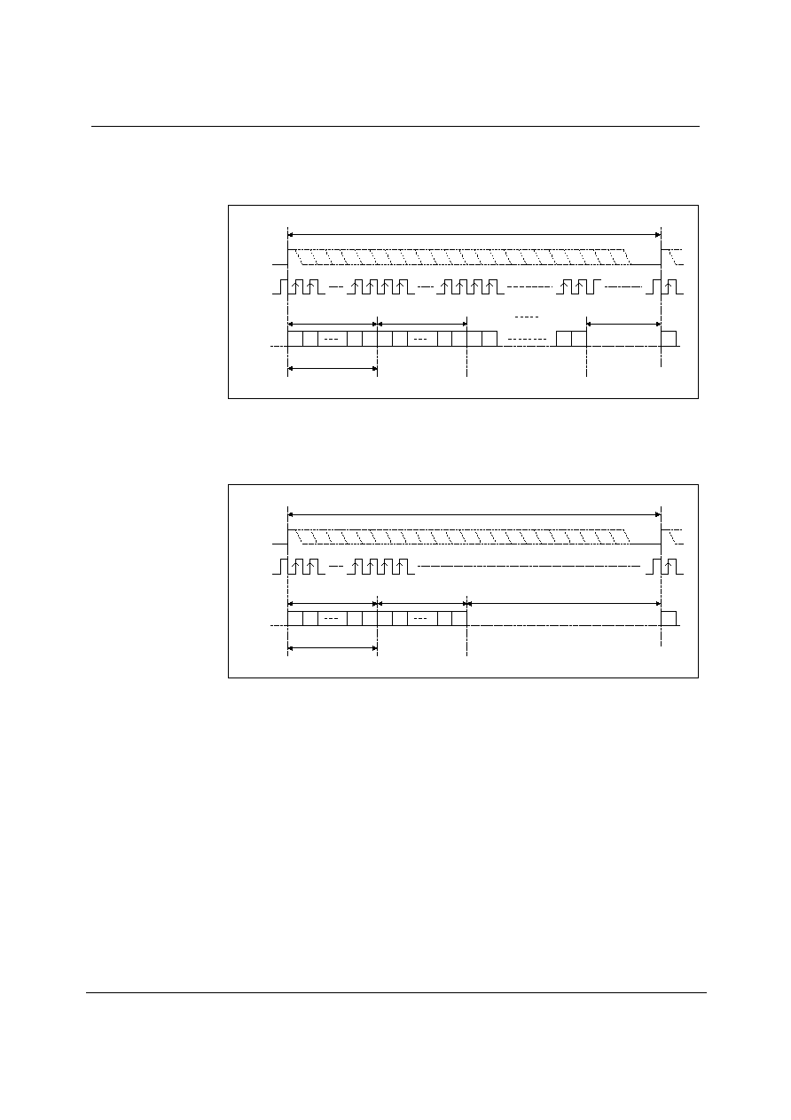
DSP EARLY MODE
In DSP early mode, the MSB of DAC channel 1 left data is sampled by the WM8770 on the second
rising edge on BCLK following a DACLRC rising edge. DAC channel 1 right and DAC channels 2, 3
and 4 data follow DAC channel 1 left data (Figure 17).
Figure 17 DSP Early Mode Timing Diagram ≠ DAC Data Input
The MSB of the left channel ADC data is output on DOUT and changes on the first falling edge of
BCLK following a low to high ADCLRC transition and may be sampled on the rising edge of BCLK.
The right channel ADC data is contiguous with the left channel data (Figure 18)
Figure 18 DSP Early Mode Timing Diagram ≠ ADC Data Output
DACLRC
BCK
DIN1
Input Word Length (IWL)
1/fs
CHANNEL 1
LEFT
n
2
1
n-1
LSB
MSB
n
2
1
n-1
CHANNEL 1
RIGHT
2
1
CHANNEL 2
LEFT
n
n-1
CHANNEL 4
RIGHT
NO VALID DATA
1 BCLK
1 BCLK
WM8770
Production Data
w
PD Rev 4.1 June 2005
24
DSP LATE MODE
In DSP late mode, the MSB of DAC channel 1 left data is sampled by the WM8770 on the first BCLK
rising edge following a DACLRC rising edge. DAC channel 1 right and DAC channels 2, 3 and 4 data
follow DAC channel 1 left data (Figure 19).
Figure 19 DSP Late Mode Timing Diagram ≠ DAC Data Input
The MSB of the left channel ADC data is output on DOUT and changes on the same falling edge of
BCLK as the low to high ADCLRC transition and may be sampled on the rising edge of BCLK. The
right channel ADC data is contiguous with the left channel data (Figure 20).
Figure 20 DSP Late Mode Timing Diagram ≠ ADC Data Output
In both early and late DSP modes, DACL1 is always sent first, followed immediately by DACR1 and
the data words for the other 6 channels. No BCLK edges are allowed between the data words. The
word order is DAC1 left, DAC1 right, DAC2 left, DAC2 right, DAC3 left, DAC3 right, DAC4 left, DAC4
right.
CONTROL INTERFACE OPERATION
The WM8770 is controlled using a 3-wire serial interface in either an SPI compatible
configuration or a CCB (Computer Control Bus) configuration.
The interface configuration is determined by the state of the CE pin on the rising edge of the
RESETB pin. If the CE pin is low on the rising edge of RESETB, CCB configuration is selected. If CE
is high on the rising edge of RESETB, SPI compatible configuration is selected.
The control interface is 5V tolerant, meaning that the control interface input signals CE, CL and DI
may have an input high level of 5V while DVDD is 3V. Input thresholds are determined by DVDD.
RESETB is also 5V tolerant.
DACLRC
BCK
DIN1
Input Word Length (IWL)
1/fs
CHANNEL 1
LEFT
n
2
1
n-1
LSB
MSB
n
2
1
n-1
CHANNEL 1
RIGHT
2
1
CHANNEL 2
LEFT
n
n-1
CHANNEL 4
RIGHT
NO VALID DATA
1
ADCLRC
BCK
DOUT
Input Word Length (IWL)
1/fs
LEFT CHANNEL
n
2
1
n-1
LSB
MSB
n
2
1
n-1
RIGHT CHANNEL
NO VALID DATA
1

Production Data
WM8770
w
PD Rev 4.1 June 2005
25
3-WIRE (SPI COMPATIBLE) SERIAL CONTROL MODE
DI is used for the program data, CL is used to clock in the program data and CE is used to latch the
program data. DI is sampled on the rising edge of CL. The 3-wire interface protocol is shown in
Figure 21.
Figure 21 3-wire SPI compatible Interface
1.
B[15:9] are Control Address Bits
2.
B[8:0] are Control Data Bits
3.
CE is edge sensitive ≠ the data is latched on the rising edge of CE.
CCB INTERFACE MODE
CCB Interface mode allows multiple devices to be controlled off a common 3-wire bus. Each device
on the 3-wire bus has its own identifying address. The WM8770 supports write only CCB interface
mode.
DI is used for the device address and program data and CL is used to clock in the address and data
on DI. DI is sampled on the rising edge of CL. CE indicates whether the data on DI is the device
address or program data. The eight clocks before a rising edge on CE will clock in the device
address. The device address is latched on the rising edge of CE. The sixteen clocks before a falling
edge on CE will clock in the program data. The program data is latched on the falling edge of CE.
A0 A1 A2 A3 A4 A5 A6 A7
D0 D1 D2 D3 D14 D15
CE
CL
DI
Figure 22 CCB Interface ≠ CL stopped low
Figure 23 CCB Interface ≠ CL stopped high
1.
A[7:0] are Device Address bits
2.
D[15:9] are Control Address bits
3.
D[8:0] are Control Data bits
The address A[7:0] for WM8770 is 8Ch (10001100).
B15 B14 B13 B12 B11 B10 B9 B8 B7 B6 B5 B4 B3 B2 B1 B0
CE
CL
DI
A0 A1 A2 A3 A4 A5 A6 A7
D0 D1 D2 D3 D14 D15
CE
CL
DI

WM8770
Production Data
w
PD Rev 4.1 June 2005
26
CONTROL INTERFACE REGISTERS
DIGITAL AUDIO INTERFACE CONTROL REGISTER
Interface format is selected via the FMT[1:0] register bits:
REGISTER ADDRESS
BIT
LABEL
DEFAULT
DESCRIPTION
10110
Interface Control
1:0
FMT[1:0]
10
Interface format Select
00 : right justified mode
01: left justified mode
10: I
2
S mode
11: DSP (early or late) mode
In left justified, right justified or I
2
S modes, the LRP register bit controls the polarity of
ADCLRC/DACLRC. If this bit is set high, the expected polarity of ADCLRC/DACLRC will be the
opposite of that shown Figure 14, Figure 15 and Figure 16. Note that if this feature is used as a
means of swapping the left and right channels, a 1 sample phase difference will be introduced. In
DSP modes, the LRP register bit is used to select between early and late modes.
REGISTER ADDRESS
BIT
LABEL
DEFAULT
DESCRIPTION
In left/right/I
2
S modes:
ADCLRC/DACLRC Polarity (normal)
0 : normal ADCLRC/DACLRC
polarity
1: inverted ADCLRC/DACLRC
polarity
10110
Interface Control
2 LRP
0
In DSP mode:
0 : Early DSP mode
1: Late DSP mode
By default, ADCLRC/DACLRC and DIN1/2/3/4 are sampled on the rising edge of BCLK and should
ideally change on the falling edge. Data sources that change ADCLRC/DACLRC and DIN1/2/3/4 on
the rising edge of BCLK can be supported by setting the BCP register bit. Setting BCP to 1 inverts
the polarity of BCLK to the inverse of that shown in Figure 14, Figure 15, Figure 16, Figure 17,
Figure 18, Figure 19 and Figure 20.
REGISTER ADDRESS
BIT
LABEL
DEFAULT
DESCRIPTION
10110
Interface Control
3
BCP
0
BCLK Polarity (DSP modes)
0 : normal BCLK polarity
1: inverted BCLK polarity
The IWL[1:0] bits are used to control the input word length.
REGISTER ADDRESS
BIT
LABEL
DEFAULT
DESCRIPTION
10110
Interface Control
5:4 WL[1:0]
10
Input
Word
Length
00 : 16 bit data
01: 20 bit data
10: 24 bit data
11: 32 bit data
Note: If 32-bit mode is selected in right justified mode, the WM8770 defaults to 24 bits.
In all modes, the data is signed 2's complement. The digital filters always input 24-bit data. If the
DAC is programmed to receive 16 or 20 bit data, the WM8770 pads the unused LSBs with zeros. If
the DAC is programmed into 32 bit mode, the 8 LSBs are ignored.
Note: In 24 bit I
2
S mode, any width of 24 bits or less is supported provided that ADCLRC/DACLRC is
high for a minimum of 24 BCLKs and low for a minimum of 24 BCLKs.
A number of options are available to control how data from the Digital Audio Interface is applied to
the DAC channels.
Control bit MS selects between audio interface Master and Slave Modes. In Master mode ADCLRC,
DACLRC and BCLK are outputs and are generated by the WM8770. In Slave mode ADCLRC,
DACLRC and BCLK are inputs to WM8770.

Production Data
WM8770
w
PD Rev 4.1 June 2005
27
REGISTER ADDRESS
BIT
LABEL
DEFAULT
DESCRIPTION
10111
Interface Control
8 MS
0
Audio
Interface
Master/Slave
Mode select:
0 : Slave Mode
1: Master Mode
MASTER MODE ADCLRC/DACLRC FREQUENCY SELECT
In Master mode the WM8770 generates ADCLRC, DACLRC and BCLK. These clocks are derived
from master clock and the ratio of MCLK to ADCLRC and DACLRC are set by ADCRATE and
DACRATE.
REGISTER ADDRESS
BIT
LABEL
DEFAULT
DESCRIPTION
2:0 ADCRATE[2:0]
010
Master
Mode
MCLK:ADCLRC
ratio select:
010: 256fs
011: 384fs
100: 512fs
101: 768fs
10111
ADCLRC and DACLRC
Frequency Select
6:4 DACRATE[2:0]
010
Master
Mode
MCLK:DACLRC
ratio select:
000: 128fs
001: 192fs
010: 256fs
011: 384fs
100: 512fs
101: 768fs
ADC OVERSAMPLING RATE SELECT
For ADC operation at 96kHz it is recommended that the user set the ADCOSR bit. This changes the
ADC signal processing oversample rate to 64fs.
REGISTER ADDRESS
BIT
LABEL
DEFAULT
DESCRIPTION
10111
ADC Oversampling
Rate
3
ADCOSR
0
ADC oversampling rate select
0: 128x oversampling
1: 64x oversampling
MUTE MODES
The WM8770 has individual mutes for each of the four DAC channels. Setting MUTE for a channel
will apply a `soft' mute to the input of the digital filters of the channel muted. DMUTE[0] mutes DAC
channel 1, DMUTE[1] mutes DAC channel 2, DMUTE[2] mutes DAC channel 3 & DMUTE[3] mutes
DAC channel 4.
REGISTER ADDRESS
BIT
LABEL
DEFAULT
DESCRIPTION
10100
Mute Control
3:0
DMUTE[3:0]
0
DAC Soft Mute select
0 : Normal Operation
1: Soft mute enabled
Setting the MUTEALL register bit will apply a 'soft' mute to the input of all the DAC digital filters:
REGISTER ADDRESS
BIT
LABEL
DEFAULT
DESCRIPTION
10100
Mute Control
4 MUTEALL
0 Soft
Mute
select
0 : Normal Operation
1: Soft mute all channels

WM8770
Production Data
w
PD Rev 4.1 June 2005
28
Figure 24 Application and Release of Soft Mute
Figure 24 shows the application and release of MUTE whilst a full amplitude sinusoid is being played
at 48kHz sampling rate. When MUTE (lower trace) is asserted, the output (upper trace) begins to
decay exponentially from the DC level of the last input sample. The output will decay towards V
MID
with a time constant of approximately 64 input samples. If MUTE is applied to all channels for 1024
or more input samples the DAC will be muted if IZD is set. When MUTE is de-asserted, the output
will restart immediately from the current input sample.
Note that all other means of muting the DAC channels: setting the PL[3:0] bits to 0, setting the
PDWN bit or setting attenuation to 0 will cause much more abrupt muting of the output.
Each ADC channel also has an individual mute control bit, which mutes the input to the ADC. In
addition both channels may be muted by setting ADCMUTE.
REGISTER ADDRESS
BIT
LABEL
DEFAULT
DESCRIPTION
11001
ADC Mute
7
ADCMUTE
0
ADC MUTE Left and Right
0 : Normal Operation
1: mute ADC left and ADC
right
11001
ADC Mute Left
5 MUTE
0
ADC
Mute
select
0 : Normal Operation
1: mute ADC left
11010
ADC Mute Right
5 MUTE
0
ADC
Mute
select
0 : Normal Operation
1: mute ADC right
The Record outputs may be enabled by setting RECEN, where RECEN enables the REC1L and
REC1R outputs.
REGISTER ADDRESS
BIT
LABEL
DEFAULT
DESCRIPTION
10100
Mute Control
5
RECEN
0
REC Output Enable
0 : REC output muted
1: REC output enabled
-2.5
-2
-1.5
-1
-0.5
0
0.5
1
1.5
0
0.001
0.002
0.003
0.004
0.005
0.006
Time(s)

Production Data
WM8770
w
PD Rev 4.1 June 2005
29
DE-EMPHASIS MODE
A digital De-emphasis filter may be applied to each DAC channel. The De-emphasis filter for each
stereo channel is enabled under the control of DEEMP[3:0]. DEEMP[0] enables the de-emphasis
filter for channel 1, DEEMP[1] enables the de-emphasis filter for channel 2, DEEMP[2] enables the
de-emphasis filter for channel 3 and DEEMP[3] enables the de-emphasis filter for channel 4.
REGISTER ADDRESS
BIT
LABEL
DEFAULT
DESCRIPTION
10101
DAC De-emphasis
Control
[3:0] DEEMPH[3:0]
0000
De-emphasis mode select:
0 : Normal Mode
1: De-emphasis Mode
Refer to Figure 34, Figure 35, Figure 36, Figure 37, Figure 38 and Figure 39 for details of the De-
Emphasis modes at different sample rates.
POWERDOWN MODE AND ADC/DAC DISABLE
Setting the PDWN register bit immediately powers down the WM8770, including the references,
overriding all other powerdown control bits. All trace of the previous input samples are removed, but
all control register settings are preserved. When PDWN is cleared the digital filters will be
reinitialised. It is recommended that the 8-channel input mux and buffer, ADC, DAC and output
mixers and EVRs are powered down before setting PDWN.
REGISTER ADDRESS
BIT
LABEL
DEFAULT
DESCRIPTION
11000
Powerdown Control
0
PDWN
0
Power Down Mode Select:
0 : Normal Mode
1: Power Down Mode
The ADC and DACs may also be powered down by setting the ADCD and DACD disable bits. Setting
ADCD will disable the ADC and select a low power mode. The ADC digital filters will be reset and will
reinitialise when ADCD is reset. Each Stereo DAC channel has a separate disable DACD[3:0].
Setting DACD for a channel will disable the DACs and select a low power mode. Resetting DACD will
reinitialise the digital filters. DACD[0] disbles DAC1, DACD[1] disables DAC2, DACD[2] disables
DAC3 and DACD[3] disables DAC4,
REGISTER ADDRESS
BIT
LABEL
DEFAULT
DESCRIPTION
1 ADCD
1 ADC
Disable:
0 : Normal Mode
1: Power Down Mode
11000
Powerdown Control
5:2 DACD[3:0]
1111 DAC
Disable:
0 : Normal Mode
1: Power Down Mode
ATTENUATOR CONTROL MODE
Setting the ATC register bit causes the left channel attenuation settings to be applied to both left and
right channel DACs from the next audio input sample. No update to the attenuation registers is
required for ATC to take effect.
REGISTER ADDRESS
BIT
LABEL
DEFAULT
DESCRIPTION
10011
DAC Channel Control
1 ATC
0
Attenuator
Control
Mode:
0 : Right channels use Right
attenuations
1: Right Channels use Left
Attenuations
WM8770
Production Data
w
PD Rev 4.1 June 2005
30
INFINITE ZERO DETECT ENABLE
Setting the IZD register bit will enable the internal infinite zero detect function:
REGISTER ADDRESS
BIT
LABEL
DEFAULT
DESCRIPTION
10011
DAC Channel Control
2
IZD
0
Infinite zero Mute Enable
0 : disable inifinite zero mute
1: enable infinite zero Mute
With IZD enabled, applying 1024 consecutive zero input samples to all 8 DAC channels will cause all
DAC outputs to be muted. Mute will be removed as soon as any channel receives a non-zero input.
ZERO FLAG OUTPUT
The DZFM control bits allow the selection of the eight DAC channel zero flag bits for output on the
ZFLAG1 and ZFLAG2 pins. A `1' on ZFLAG1 or ZFLAG2 indicates 1024 consecutive zero input
samples to the channels selected.
REGISTER ADDRESS
BIT
LABEL
DEFAULT
DESCRIPTION
10101
Zero Flag Select
7:4
DZFM[3:0]
0000
Selects the ouput for ZFLAG1
and ZFLAG2 pins (see Table 9).
A `1' indicates 1024 consecutive
zero input samples on the
channels selected.
DAC OUTPUT CONTROL
The DAC output control word determines how the left and right inputs to the audio Interface are
applied to the left and right DACs:
REGISTER ADDRESS
BIT
LABEL
DEFAULT
DESCRIPTION
PL[3:0] Left
Output
Right
Output
0000 Mute Mute
0001 Left Mute
0010 Right Mute
0011 (L+R)/2
Mute
0100 Mute Left
0101 Left Left
0110 Right Left
0111 (L+R)/2
Left
1000 Mute Right
1001 Left Right
1010 Right Right
1011 (L+R)/2
Right
1100 Mute (L+R)/2
1101 Left (L+R)/2
1110 Right (L+R)/2
10011
DAC Control
7:4 PL[3:0]
1001
1111 (L+R)/2
(L+R)/2

Production Data
WM8770
w
PD Rev 4.1 June 2005
31
DAC ANALOGUE VOLUME CONTROL
The DAC volume may be adjusted independently in both the analogue and digital domain using
separate volume control registers.
REGISTER
ADDRESS
BIT LABEL DEFAULT
DESCRIPTION
6:0
L1A[6:0] 1111111
(0dB)
Attenuation data for Left channel DACL1 in 1dB steps. See Table 11
7
L1ZCEN 0 DACL1 zero cross detect enable
0: zero cross disabled
1: zero cross enabled
00000
Analogue
Attenuation
DACL1
8
UPDATE Not
latched Controls simultaneous update of all Attenuation Latches
0: Store L1A in intermediate latch (no change to output)
1: Store L1A and update attenuation on all channels.
6:0
R1A[6:0] 1111111
(0dB)
Attenuation data for Right channel DACR1 in 1dB steps. See Table
11
7
R1ZCEN 0 DACR1 zero cross detect enable
0: zero cross disabled
1: zero cross enabled
00001
Analogue
Attenuation
DACR1
8
UPDATE Not
latched Controls simultaneous update of all Attenuation Latches
0: Store R1A in intermediate latch (no change to output)
1: Store R1A and update attenuation on all channels.
6:0
L2A[6:0] 1111111
(0dB)
Attenuation data for Left channel DACL2 in 1dB steps. See Table 11
7
L2ZCEN 0 DACL2 zero cross detect enable
0: zero cross disabled
1: zero cross enabled
00010
Analogue
Attenuation
DACL2
8
UPDATE Not
latched Controls simultaneous update of all Attenuation Latches
0: Store L2A in intermediate latch (no change to output)
1: Store L2A and update attenuation on all channels.
6:0
R2A[6:0] 1111111
(0dB)
Attenuation data for Right channel DACR2 in 1dB steps. See Table
11
7
R2ZCEN 0 DACR2 zero cross detect enable
0: zero cross disabled
1: zero cross enabled
00011
Analogue
Attenuation
DACR2
8
UPDATE Not
latched Controls simultaneous update of all Attenuation Latches
0: Store R2A in intermediate latch (no change to output)
1: Store R2A and update attenuation on all channels.
6:0
L3A[6:0] 1111111
(0dB)
Attenuation data for Left channel DACL3 in 1dB steps. See Table 11
7
L3ZCEN 0 DACL3 zero cross detect enable
0: zero cross disabled
1: zero cross enabled
00100
Analogue
Attenuation
DACL3
8
UPDATE Not
latched Controls simultaneous update of all Attenuation Latches
0: Store L3A in intermediate latch (no change to output)
1: Store L3A and update attenuation on all channels.
6:0
R3A[6:0] 1111111
(0dB)
Attenuation data for Right channel DACL3 in 1dB steps. See Table
11
7
R3ZCEN 0 DACR3 zero cross detect enable
0: zero cross disabled
1: zero cross enabled
00101
Analogue
Attenuation
DACR3
8
UPDATE Not
latched Controls simultaneous update of all Attenuation Latches
0: Store R3A in intermediate latch (no change to output)
1: Store R3A and update attenuation on all channels.

WM8770
Production Data
w
PD Rev 4.1 June 2005
32
REGISTER
ADDRESS
BIT LABEL DEFAULT
DESCRIPTION
6:0
L4A[6:0] 1111111
(0dB)
Attenuation data for Left channel DACL4 in 1dB steps. See Table 11
7
L4ZCEN 0 DACL4 zero cross detect enable
0: zero cross disabled
1: zero cross enabled
00110
Analogue
Attenuation
DACL4
8
UPDATE
Not latched
Controls simultaneous update of all Attenuation Latches
0: Store L4A in intermediate latch (no change to output)
1: Store L4A and update attenuation on all channels.
6:0
R4A[6:0] 1111111
(0dB)
Attenuation data for Right channel DACL4 in 1dB steps. See Table
11
7
R4ZCEN 0 DACR4 zero cross detect enable
0: zero cross disabled
1: zero cross enabled
00111
Analogue
Attenuation
DACR4
8
UPDATE Not
latched Controls simultaneous update of all Attenuation Latches
0: Store R4A in intermediate latch (no change to output)
1: Store R4A and update attenuation on all channels.
6:0
MASTA[6:0] 1111111
(0dB)
Attenuation data for all channel DAC in 1dB steps. See Table 11
7
MZCEN 0 Master zero cross detect enable
0: zero cross disabled
1: zero cross enabled
01000
Master
Analogue
Attenuation
(all channels)
8
UPDATE Not
latched Controls simultaneous update of all Attenuation Latches
0: Store gain in intermediate latch (no change to output)
1: Store gain and update attenuation on all channels.
Table 10 Attenuation Register Map
Each DAC channel volume can be controlled digitally in an analogue volume stage after the DAC.
Attenuation is 0dB by default but can be set between 0 and ≠100dB in 1dB steps using the 7
Attenuation control words. All attenuation registers are double latched allowing new values to be pre-
latched to several channels before being updated synchronously. Setting the UPDATE bit on any
attenuation write will cause all pre-latched values to be immediately applied to the DAC channels. A
master attenuation register is also included, allowing all volume levels to be set to the same value in
a single write.
Note: The UPDATE bit is not latched. If UPDATE=0, the Attenuation value will be written to the pre-
latch but not applied to the relevant DAC. If UPDATE=1, all pre-latched values will be applied from
the next input sample. Writing to MASTA[6:0] overwrites any values previously sent to L1A[6:0],
L2A[6:0], L3A[6:0], L4A[6:0], R1A[6:0], R2A[6:0], R3A[6:0], R4A[6:0].
In addition a zero cross detect circuit is provided for each DAC volume under the control of bit 7
(xZCEN) in each DAC attenuation register. When ZCEN is set the attenuation values are only
updated when the input signal to the gain stage is close to the analogue ground level. This minimises
audible clicks and `zipper' noise as the gain values change. A timeout clock is also provided which
will generate an update after a minimum of 131072 master clocks (= ~10.5ms with a master clock of
12.288MHz). The timeout clock may be disabled by setting TOD.
REGISTER ADDRESS
BIT
LABEL
DEFAULT
DESCRIPTION
10011
Timeout Clock Disable
3
TOD 0
DAC Analogue Zero cross detect
timeout disable
0 : Timeout enabled
1: Timeout disabled
Production Data
WM8770
w
PD Rev 4.1 June 2005
33
DAC ANALOGUE OUTPUT ATTENUATION
Register bits L1A and R1A control the left and right channel attenuation of DAC 1. Register bits L2A
and R2A control the left and right channel attenuation of DAC 2. Register bits L3A and R3A control
the left and right channel attenuation of DAC 3. Register bits L4A and R4A control the left and right
channel attenuation of DAC 4. Register bits MASTA can be used to control attenuation of all
channels.
Table 8 shows how the attenuation levels are selected from the 7-bit words.
L/RA
x
[6:0] ATTENUATION
LEVEL
00(hex) -
dB (mute)
: :
1A(hex) -
dB (mute)
1B(hex) -100dB
: :
7D(hex) -2dB
7E(hex) -1dB
7F(hex) 0dB
Table 11 Analogue Volume Control Attenuation Levels
DAC DIGITAL VOLUME CONTROL
The DAC volume may also be adjusted in the digital domain using independent digtal attenuation
control registers
REGISTER
ADDRESS
BIT LABEL DEFAULT
DESCRIPTION
7:0
LDA1[7:0] 11111111
(0dB)
Digital Attenuation data for Left channel DACL1 in 0.5dB steps. See
Table 12
01001
Digital
Attenuation
DACL1
8
UPDATE Not
latched Controls simultaneous update of all Attenuation Latches
0: Store LDA1 in intermediate latch (no change to output)
1: Store LDA1 and update attenuation on all channels
7:0
RDA1[6:0] 11111111
(0dB)
Digital Attenuation data for Right channel DACR1 in 0.5dB steps.
See Table 12
01010
Digital
Attenuation
DACR1
8
UPDATE Not
latched Controls simultaneous update of all Attenuation Latches
0: Store RDA1 in intermediate latch (no change to output)
1: Store RDA1 and update attenuation on all channels.
7:0
LDA2[7:0] 11111111
(0dB)
Digital Attenuation data for Left channel DACL2 in 0.5dB steps. See
Table 12
01011
Digital
Attenuation
DACL2
8
UPDATE Not
latched Controls simultaneous update of all Attenuation Latches
0: Store LDA2 in intermediate latch (no change to output)
1: Store LDA2 and update attenuation on all channels.
7:0
RDA2[7:0] 11111111
(0dB)
Digital Attenuation data for Right channel DACR2 in 0.5dB steps.
See Table 12
01100
Digital
Attenuation
DACR2
8
UPDATE Not
latched Controls simultaneous update of all Attenuation Latches
0: Store RDA2 in intermediate latch (no change to output)
1: Store RDA2 and update attenuation on all channels.
7:0
LDA3[7:0] 11111111
(0dB)
Digital Attenuation data for Left channel DACL3 in 0.5dB steps. See
Table 12
01101
Digital
Attenuation
DACL3
8
UPDATE Not
latched Controls simultaneous update of all Attenuation Latches
0: Store LDA3 in intermediate latch (no change to output)
1: Store LDA3 and update attenuation on all channels.
7:0
RDA3[7:0] 11111111
(0dB)
Digital Attenuation data for Right channel DACR3 in 0.5dB steps.
See Table 12
01110
Digital
Attenuation
DACR3
8
UPDATE Not
latched Controls simultaneous update of all Attenuation Latches
0: Store RDA3 in intermediate latch (no change to output)
1: Store RDA3 and update attenuation on all channels.

WM8770
Production Data
w
PD Rev 4.1 June 2005
34
REGISTER
ADDRESS
BIT LABEL DEFAULT
DESCRIPTION
7:0
LDA4[7:0] 11111111
(0dB)
Digital Attenuation data for Left channel DACL4 in 0.5dB steps. See
Table 12
01111
Digital
Attenuation
DACL4
8
UPDATE Not
latched Controls simultaneous update of all Attenuation Latches
0: Store LDA4 in intermediate latch (no change to output)
1: Store LDA4 and update attenuation on all channels.
7:0
RDA4[7:0] 11111111
(0dB)
Digital Attenuation data for Right channel DACR4 in 0.5dB steps.
See Table 12
10000
Digital
Attenuation
DACR4
8
UPDATE Not
latched Controls simultaneous update of all Attenuation Latches
0: Store RDA4 in intermediate latch (no change to output)
1: Store RDA4 and update attenuation on all channels.
7:0
MASTDA[7:0] 11111111
(0dB)
Digital Attenuation data for all DAC channels in 0.5dB steps. See
Table 12
10001
Master
Digital
Attenuation
(all channels)
8
UPDATE Not
latched Controls simultaneous update of all Attenuation Latches
0: Store gain in intermediate latch (no change to output)
1: Store gain and update attenuation on all channels.
L/RDAX[7:0] ATTENUATION
LEVEL
00(hex) -
dB (mute)
01(hex) -127.5dB
: :
: :
: :
FE(hex) -0.5dB
FF(hex) 0dB
Table 12 Digital Volume Control Attenuation Levels
The Digital volume control also incorporates a zero cross detect circuit which detects a transition
through the zero point before updating the digital volume control with the new volume. This is
enabled by control bit DZCEN.
REGISTER ADDRESS
BIT
LABEL
DEFAULT
DESCRIPTION
10011
DAC Control
0
DZCEN 0 DAC
Digital
Volume
Zero
Cross
Enable:
0: Zero cross detect disabled
1: Zero cross detect enabled

Production Data
WM8770
w
PD Rev 4.1 June 2005
35
DAC OUTPUT PHASE
The DAC Phase control word determines whether the output of each DAC is non-inverted or inverted
REGISTER
ADDRESS
BIT LABEL
DEFAULT
DESCRIPTION
Bit DAC
Phase
0 DAC1L
1
=
invert
1 DAC1R
1
=
invert
2 DAC2L
1
=
invert
3 DAC2R
1
=
invert
4 DAC3L
1
=
invert
5 DAC3R
1
=
invert
6 DAC4L
1
=
invert
10010
DAC Phase
7:0 PH[7:0]
00000000
7 DAC4R
1
=
invert
ADC GAIN CONTROL
Control bits LAG[4:0] and RAG[4:0] control the ADC input gain, allowing the user to attenuate the
ADC input signal to match the full-scale range of the ADC. The gain is independently adjustable on
left and right inputs. Left and right inputs may also be independently muted. The LRBOTH control bit
allows the user to write the same attenuation value to both left and right volume control registers. The
ADC volume and mute also applies to the bypass signal path.
REGISTER
ADDRESS
BIT LABEL DEFAULT
DESCRIPTION
4:0
LAG[4:0] 01100
(0dB)
Attenuation data for Left channel ADC gain in 1dB steps. See Table
13
5
MUTE 0
Mute for Left channel ADC:
0: Mute off
1: Mute on
11001
Attenuation
ADCL
6
LRBOTH 0 Setting LRBOTH will write the same gain value to LAG[4:0] and
RAG[4:0]
4:0
RAG[4:0] 01100
(0dB)
Attenuation data for right channel ADC gain in 1dB steps. See Table
13
5
MUTE 0
Mute for RIght channel ADC:
0: Mute off
1: Mute on
11010
Attenuation
ADCR
6
LRBOTH 0 Setting LRBOTH will write the same gain value to RAG[4:0] and
LAG[4:0]
ADC INPUT GAIN
Registers LAG and RAG control the left and right channel gain into the stereo ADC in 1dB steps from
+19dB to ≠12dB Table 8 shows how the attenuation levels are selected from the 5-bit words.
L/RAG[6:0] ATTENUATION
LEVEL
0 -12dB
: :
01100 0dB
: :
11111 +19dB
Table 13 ADC Gain Control
WM8770
Production Data
w
PD Rev 4.1 June 2005
36
ADC HIGHPASS FILTER DISABLE
The ADC digital filters contain a digital highpass filter. This defaults to enabled and can be disabled
using software control bit ADCHPD.
REGISTER ADDRESS
BIT
LABEL
DEFAULT
DESCRIPTION
10110
ADC control
8
ADCHPD
0
ADC Highpass filter disable:
0: Highpass filter enabled
1: Highpass filter disabled
ADC INPUT MUX AND POWERDOWN CONTROL
REGISTER
ADDRESS
BIT LABEL
DEFAULT
DESCRIPTION
2:0
LMX[2:0] 000
ADC left channel input mux control
bits (see Table 14)
6:4
RMX[2:0] 000
ADC right channel input mux
control bits (see Table 14)
11011
ADC Mux and
Powerdown
Control
8
AINPD 1 Input mux and buffer powerdown
0: Input mux and buffer
enabled
1: Input mux and buffer
powered down
Register bits LMX and RMX control the left and right channel inputs into the stereo ADC. The default
is AIN1. However if the analogue input buffer is powered down, by setting AINPD, then all 8-channel
mux inputs are switched to buffered VMIDADC.
LMX[2:0] LEFT
ADC
INPUT
RMX[2:0]
RIGHT ADC INPUT
000 AIN1L 000 AIN1R
001 AIN2L 001 AIN2R
010 AIN3L 010 AIN3R
011 AIN4L 011 AIN4R
100 AIN5L 100 AIN5R
101 AIN6L 101 AIN6R
110 AIN7L 110 AIN7R
111 AIN8L 111 AIN8R
Table 14 ADC Input Mux Control
OUTPUT SELECT AND ENABLE CONTROL
Register bits MX1 to MX4 control the output select. The output select block consists of a summing
stage and an input select switch for each input allowing each signal to be output individually or
summed with other signals and output on each analogue output. The default for all outputs is DAC
playback only. VOUT1/2/3 may be selected to output DAC playback, AUX, analogue bypass or a
sum of these using the output select controls MX1/2/3[2:0]. VOUT4 may be selected to output DAC
playback, analogue bypass or a sum of these signals using MX4[1:0]. It is recommended that bypass
is not selected for output on more than two stereo channels simultaneously to avoid overloading the
input buffer, resulting in a decrease in performance.
The output mixers and EVRs can be powered down under control of OUTPD[3:0]. Each stereo
channel may be powered down separately. Setting OUTPD[3:0] will power off the mixer and EVR and
switch the analogue outputs VOUTL/R to VMIDDAC to maintain a dc level on the output.
When setting OUTPD MX1/2/3/4 should be set to deselect all signals.
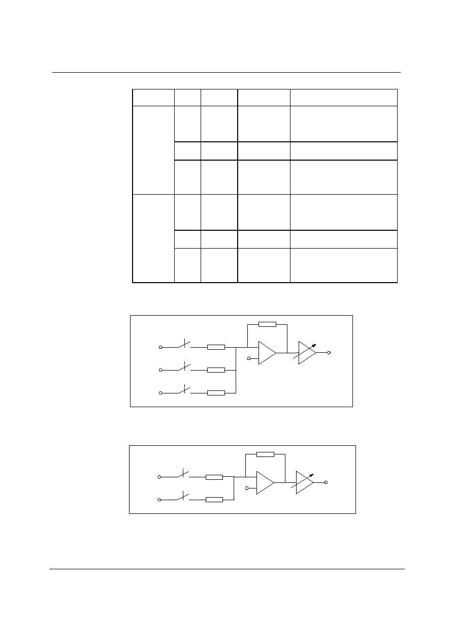
Production Data
WM8770
w
PD Rev 4.1 June 2005
37
REGISTER
ADDRESS
BIT LABEL DEFAULT
DESCRIPTION
2:0
MX1[2:0] 001
(DAC playback)
VOUT1 Output select (see
Figure 25)
5:3
MX2[2:0] 001
(DAC playback)
VOUT2 Output select (see Figure 25)
11100
Output Mux
and
Powerdown
Control
8:7
OUTPD[1:0] 11
Mixer and EVR Powerdown select
0: mixer and EVR enabled
1: mixer and EVR powered
down
2:0
MX3[2:0] 001
(DAC playback)
VOUT3 Output select (see
Figure 25)
4:3
MX4[1:0] 01
(DAC playback)
VOUT4 Output select (see Figure 26)
11101
Output Mux
and
Powerdown
Control
8:7
OUTPD[3:2] 11
Mixer and EVR Powerdown select
0: mixer and EVR enabled
1: mixer and EVR powered
down
MX1/2/3[2:0] selects the output for VOUT1/2/3.
Figure 25 MX1/2/3[2:0] Output Select
MX4[1:0] selects the output for VOUT4L/R.
Figure 26 MX4[1:0] Output Select
SOFTWARE REGISTER RESET
Wrting to register 11111 will cause a register reset, resetting all register bits to their default values.
MX4[0]
MX4[1]
DAC4
BYPASS
VOUT4
MX[0]
MX[1]
MX[2]
DAC
AUX
BYPASS
VOUT

WM8770
Production Data
w
PD Rev 4.1 June 2005
38
REGISTER MAP
The complete register map is shown below. The detailed description can be found in the relevant text of the device description. The
WM8770 can be configured using the Control Interface. All unused bits should be set to `0'.
REGISTER B15 B14 B13 B12 B11 B10 B9 B8
B7
B6
B5
B4
B3
B2
B1
B0
DEFAULT
R0(00h)
0
0
0
0
0
0
0
UPDATE L1ZCEN
L1A[6:0]
X01111111
R1(01h)
0
0
0
0
0
0
1
UPDATE R1ZCEN
R1A[6:0]
X01111111
R2(02h)
0
0
0
0
0
1
0
UPDATE L2ZCEN
L2A[6:0]
X01111111
R3(03h)
0
0
0
0
0
1
1
UPDATE R2ZCEN
R2A[6:0]
X01111111
R4(04h)
0
0
0
0
1
0
0
UPDATE L3ZCEN
L3A[6:0]
X01111111
R5(05h)
0
0
0
0
1
0
1
UPDATE R3ZCEN
R3A[6:0]
X01111111
R6(06h)
0
0
0
0
1
1
0
UPDATE L4ZCEN
L4A[6:0]
X01111111
R7(07h)
0
0
0
0
1
1
1
UPDATE R4ZCEN
R4A[6:0]
X01111111
R8(08h)
0
0
0
1
0
0
0
UPDATE MZCEN
MASTA[6:0]
X01111111
R9(09h)
0
0
0
1
0
0
1
UPDATE LDA1[7:0] X11111111
R10(0Ah)
0
0
0
1
0
1
0
UPDATE RDA1[7:0] X11111111
R11(0Bh)
0
0
0
1
0
1
1
UPDATE LDA2[7:0] X11111111
R12(0Ch)
0
0
0
1
1
0
0
UPDATE RDA2[7:0] X11111111
R13(0Dh)
0
0
0
1
1
0
1
UPDATE LDA3[7:0] X11111111
R14(0Eh)
0
0
0
1
1
1
0
UPDATE RDA3[7:0] X11111111
R15(0Fh)
0
0
0
1
1
1
1
UPDATE LDA4[7:0] X11111111
R16(10h)
0
0
1
0
0
0
0
UPDATE RDA4[7:0] X11111111
R17(11h)
0
0
1
0
0
0
1
UPDATE MASTDA[7:0] X11111111
R18(12h)
0
0
1
0
0
1
0
0 PHASE[7:0]
000000000
R19(13h)
0
0
1
0
0
1
1
0 PL
TOD
IZD
ATC
DZCEN
010010000
R20(14h)
0
0
1
0
1
0
0
0 0 0
RECEN
MUTEALL DMUTE[3:0] 000000000
R21(15h)
0
0
1
0
1
0
1
0 DZFM[3:0]
DEEMP[3:0]
000000000
R22(16h)
0
0
1
0
1
1
0
ADCHPD 0
0
WL[1:0]
BCP
LRP FMT[1:0] 000100010
R23(17h)
0
0
1
0
1
1
1
MS 0
DACRATE[2:0] ADCOSR ADCRATE[2:0] 000100010
R24(18h)
0
0
1
1
0
0
0
0 0 0
DACD[3:0]
ADCD
PWDN
000111110
R25(19h)
0
0
1
1
0
0
1
0 ADCMUTE
LRBOTH MUTE
LAG[4:0]
000001100
R26(1Ah)
0
0
1
1
0
1
0
0 0
LRBOTH MUTE
RAG[4:0]
000001100
R27(1Bh)
0
0
1
1
0
1
1
AINPD 0
RMX[2:0]
0
LMX[2:0]
100000000
R28(1Ch)
0
0
1
1
1
0
0
OUTPD[1:0] 0
MX2[2:0]
MX1[2:0] 110001001
R29(1Dh)
0
0
1
1
1
0
1
OUTPD[3:2] 0
0 MX4[1:0]
MX3[2:0] 110001001
R31(1Fh)
0
0
1
1
1
1
1
RESET not
reset
ADDRESS
DATA DEFAULT

Production Data
WM8770
w
PD Rev 4.1 June 2005
39
REGISTER
ADDRESS
BIT LABEL DEFAULT
DESCRIPTION
6:0
L1A[6:0] 1111111
(0dB)
Attenuation Data for Left Channel DACL1 in 1dB steps. See Table
11
7
L1ZCEN 0
DACL1 Zero Cross Detect Enable
0: zero cross disabled
1: zero cross enabled
00000
Analogue
Attenuation
DACL1
8
UPDATE Not
latched
Controls simultaneous update of all Attenuation Latches
0: Store DACL1 in intermediate latch (no change to output)
1: Store DACL1 and update attenuation on all channels.
6:0
R1A[6:0] 1111111
(0dB)
Attenuation Data for Left channel DACL1 in 1dB steps. See Table
11
7
R1ZCEN 0
DACR1 Zero Cross Detect Enable
0: zero cross disabled
1: zero cross enabled
00001
Analogue
Attenuation
DACR1
8
UPDATE Not
latched
Controls simultaneous update of all Attenuation Latches
0: Store DACR1 in intermediate latch (no change to output)
1: Store DACR1 and update attenuation on all channels.
6:0
L2A[6:0] 1111111
(0dB)
Attenuation Data for Left Channel DACL2 in 1dB Steps. See
Table 11
7
L2ZCEN 0
DACL2 Zero Cross Detect Enable
0: zero cross disabled
1: zero cross enabled
00010
Analogue
Attenuation
DACL2
8
UPDATE
Not latched
Controls simultaneous update of all Attenuation Latches
0: Store DACL2 in intermediate latch (no change to output)
1: Store DACL2 and update attenuation on all channels.
6:0
R2A[6:0]
1111111
(0dB)
Attenuation Data for Right Channel DACR2 in 1dB steps. See
Table 11
7
R2ZCEN 0
DACR2 Zero Cross Detect Enable
0: zero cross disabled
1: zero cross enabled
00011
Analogue
Attenuation
DACR2
8
UPDATE
Not latched
Controls simultaneous update of all Attenuation Latches
0: Store DACR2 in intermediate latch (no change to output)
1: Store DACR2 and update attenuation on all channels.
6:0 L3A[6:0] 1111111
(0dB)
Attenuation Data for Left channel DACL3 in 1dB steps. See Table
11
7
L3ZCEN 0
DACL2 Zero Cross Detect Enable
0: zero cross disabled
1: zero cross enabled
00100
Analogue
Attenuation
DACL3
8
UPDATE
Not latched
Controls simultaneous update of all Attenuation Latches
0: Store DACL3 in intermediate latch (no change to output)
1: Store DACL3 and update attenuation on all channels.
6:0 R3A[6:0] 1111111
(0dB)
Attenuation Data for Left channel DACL3 in 1dB steps. Table 11
7
R3ZCEN 0
DACR2 Zero Cross Detect Enable
0: zero cross disabled
1: zero cross enabled
00101
Analogue
Attenuation
DACR3
8
UPDATE
Not latched
Controls simultaneous update of all Attenuation Latches
0: Store DACR3 in intermediate latch (no change to output)
1: Store DACR3 and update attenuation on all channels.

WM8770
Production Data
w
PD Rev 4.1 June 2005
40
REGISTER
ADDRESS
BIT LABEL DEFAULT
DESCRIPTION
6:0
L4A[6:0] 1111111
(0dB)
Attenuation Data for Left Channel DACL4 in 1dB steps. See Table
11
7
L4ZCEN 0
DACL2 Zero Cross Detect Enable
0: zero cross disabled
1: zero cross enabled
00110
Analogue
Attenuation
DACL4
8
UPDATE Not
latched
Controls simultaneous update of all Attenuation Latches
0: Store DACL4 in intermediate latch (no change to output)
1: Store DACL4 and update attenuation on all channels.
6:0
R4A[6:0] 1111111
(0dB)
Attenuation Data for Left Channel DACL4 in 1dB steps. See Table
11
7
R4ZCEN 0
DACR2 Zero Cross Detect Enable
0: zero cross disabled
1: zero cross enabled
00111
Analogue
Attenuation
DACR4
8
UPDATE Not
latched
Controls simultaneous update of all Attenuation Latches
0: Store DACR4 in intermediate latch (no change to output)
1: Store DACR4 and update attenuation on all channels.
6:0
MASTA[6:0] 1111111
(0dB)
Attenuation Data for all DAC Gains in 1dB steps. See Table 11
7
MZCEN 0
Master Zero Cross Detect Enable
0: zero cross disabled
1: zero cross enabled
01000
Analogue
Master
Attenuation
(all channels)
8
UPDATE Not
latched
Controls simultaneous update of all Attenuation Latches
0: Store gains in intermediate latch (no change to output)
1: Store gains and update attenuation on all channels.
7:0
LDA1[7:0] 11111111
(0dB)
Digital Attenuation Data for Left Channel DACL1 in 0.5dB steps.
See Table 12
01001
Digital
Attenuation
DACL1
8
UPDATE Not
latched
Controls simultaneous Update of all Attenuation Latches
0: Store LDA1 in intermediate latch (no change to output)
1: Store LDA1 and update attenuation on all channels
7:0
RDA1[6:0] 11111111
(0dB)
Digital Attenuation Data for Right Channel DACR1 in 0.5dB steps.
See Table 12
01010
Digital
Attenuation
DACR1
8
UPDATE Not
latched
Controls simultaneous update of all Attenuation Latches
0: Store RDA1 in intermediate latch (no change to output)
1: Store RDA1 and update attenuation on all channels.
7:0
LDA2[7:0] 11111111
(0dB)
Digital Attenuation data for Left channel DACL2 in 0.5dB steps.
See Table 12
01011
Digital
Attenuation
DACL2
8
UPDATE Not
latched
Controls simultaneous update of all Attenuation Latches
0: Store LDA2 in intermediate latch (no change to output)
1: Store LDA2 and update attenuation on all channels.
7:0
RDA2[7:0] 11111111
(0dB)
Digital Attenuation Data for Right Channel DACR2 in 0.5dB steps.
See Table 12
01100
Digital
Attenuation
DACR2
8
UPDATE Not
latched
Controls simultaneous update of all Attenuation Latches
0: Store RDA2 in intermediate latch (no change to output)
1: Store RDA2 and update attenuation on all channels.
7:0
LDA3[7:0] 11111111
(0dB)
Digital Attenuation Data for Left Channel DACL3 in 0.5dB steps.
See Table 12
01101
Digital
Attenuation
DACL3
8
UPDATE Not
latched
Controls simultaneous update of all Attenuation Latches
0: Store LDA3 in intermediate latch (no change to output)
1: Store LDA3 and update attenuation on all channels.

Production Data
WM8770
w
PD Rev 4.1 June 2005
41
REGISTER
ADDRESS
BIT LABEL DEFAULT
DESCRIPTION
7:0
RDA3[7:0] 11111111
(0dB)
Digital Attenuation Data for Right channel DACR3 in 0.5dB steps.
See Table 12
01110
Digital
Attenuation
DACR3
8
UPDATE Not
latched
Controls simultaneous update of all Attenuation Latches
0: Store RDA3 in intermediate latch (no change to output)
1: Store RDA3 and update attenuation on all channels.
7:0
LDA4[7:0] 11111111
(0dB)
Digital Attenuation Data for Left Channel DACL4 in 0.5dB steps.
See Table 12
01111
Digital
Attenuation
DACL4
8
UPDATE Not
latched
Controls simultaneous update of all Attenuation Latches
0: Store LDA4 in intermediate latch (no change to output)
1: Store LDA4 and update attenuation on all channels.
7:0
RDA4[7:0] 11111111
(0dB)
Digital Attenuation Data for Right Channel DACR4 in 0.5dB steps.
See Table 12
10000
Digital
Attenuation
DACR4
8
UPDATE Not
latched
Controls simultaneous update of all Attenuation Latches
0: Store RDA4 in intermediate latch (no change to output)
1: Store RDA4 and update attenuation on all channels.
7:0
MASTDA[7:0] 11111111
(0dB)
Digital Attenuation Data for all DAC Channels in 0.5dB steps. See
Table 12
10001
Master
Digital
Attenuation
(all channels)
8
UPDATE Not
latched
Controls simultaneous update of all Attenuation Latches
0: Store gain in intermediate latch (no change to output)
1: Store gain and update attenuation on all channels.
10010
Phase swaps
7:0
PHASE
00000000
Controls Phase of DAC Outputs
0: Sets non inverted output phase
1: inverts phase of DAC output
0
DZCEN 0
DAC Digital Volume Zero Cross Enable:
0: Zero Cross detect disabled
1: Zero Cross detect enabled
1
ATC 0
Attenuator Control
0: All DACs use attenuations as programmed.
1: Right channel DACs use corresponding left DAC
attenuations
2
IZD 0
Infinite Zero Detection Circuit Control and Automute Control
0: Infinite zero detect automute disabled
1: Infinite zero detect automute enabled
3 TOD
0
DAC Analogue Zero Cross Detect Timeout Disable
0 : Timeout enabled
1: Timeout disabled
DAC Output Control
PL[3:0] Left
Output
Right
Output
PL[3:0] Left
Output
Right
Output
0000 Mute Mute 1000 Mute Right
0001 Left Mute 1001 Left Right
0010 Right Mute 1010 Right Right
0011 (L+R)/2
Mute 1011 (L+R)/2
Right
0100 Mute Left 1100 Mute (L+R)/2
0101 Left Left 1101 Left (L+R)/2
0110 Right Left 1110 Right (L+R)/2
10011
DAC Control
7:4 PL[3:0] 1001
0111 (L+R)/2
Left 1111 (L+R)/2
(L+R)/2

WM8770
Production Data
w
PD Rev 4.1 June 2005
42
REGISTER
ADDRESS
BIT LABEL DEFAULT
DESCRIPTION
3:0
DMUTE[3:0] 0000
DAC Channel Soft Mute Enables:
0: mute disabled
1: mute enabled
4
MUTEALL 0
DAC Channel Master Soft Mute. Mutes all DAC channels:
0: mute disabled
1: mute enabled
10100
Mute Control
5
RECEN
0
REC Output Enable
0 : REC output muted
1: REC output enabled
3:0
DEEMP[3:0]
0000
De-emphasis Mode Select:
0 : Normal Mode
1: De-emphasis Mode
10101
DAC Control
7:4
DZFM[3:0] 0000
Selects the ouput for ZFLG1 and ZFLG2 pins (see Table 9).
1: indicates 1024 consecutive zero input samples on the
channels selected
0: indicates at least one of selected channels has non
zero sample in last 1024 inputs
1:0
FMT[1:0]
10
Interface Format Select
00: right justified mode
01: left justified mode
10: I
2
S mode
11: DSP mode
ADCLRC/DACLRC Polarity or DSP Early/Late mode select
2 LRP
0
Left Justified / Right Justified /
I
2
S
0: Standard DACLRC Polarity
1: Inverted DACLRC Polarity
DSP Mode
0: Early DSP mode
1: Late DSP mode
3 BCP
0
BITCLK
Polarity
0: Normal - DIN[3:0], DACLRC & ADCLRC sampled on
rising edge of BCLK; DOUT changes on falling edge of
BCLK.
1: Inverted - DIN[3:0], DACLRC & ADCLRC sampled on
falling edge of BCLK; DOUT changes on rising edge of
BCLK.
5:4 WL[1:0]
10 Input
Word
Length
00: 16-bit Mode
01: 20-bit Mode
10: 24-bit Mode
11: 32-bit Mode (not supported in right justified mode)
10110
Interface
Control
8
ADCHPD
0
ADC Highpass Filter Disable:
0: Highpass Filter enabled
1: Highpass Filter disabled

Production Data
WM8770
w
PD Rev 4.1 June 2005
43
REGISTER
ADDRESS
BIT LABEL DEFAULT
DESCRIPTION
2:0 ADCRATE[2:0]
010
Master Mode MCLK:ADCLRC Ratio Select:
010: 256fs
011: 384fs
100: 512fs
3 ADCOSR
0 ADC oversample rate select
0: 128x oversampling
1: 64x oversapmling
6:4 DACRATE[2:0]
010
Master Mode MCLK:DACLRC Ratio Select:
000: 128fs
001: 192fs
010: 256fs
011: 384fs
100: 512fs
10111
Master Mode
Control
8
MS
0
Maser/Slave Interface Mode Select
0: Slave Mode ≠ ADCLRC, DACLRC and BCLK are inputs
1: Master Mode ≠ ADCLRC, DACLRC and BCLK are outputs
0
PWDN
0
Chip Powerdown Control (works in tandem with ADCD and
DACD):
0: All circuits running, outputs are active
1: All circuits in power save mode, outputs muted
1 ADCD
1
ADC
Powerdown:
0: ADC enabled
1: ADC disabled
11000
Powerdown
Control
5:2 DACD[3:0]
1111 DAC
Powerdown
0: DAC enabled
1: DAC disabled
4:0 LAG[4:0] 01100
(0dB)
Attenuation Data for Left Channel ADC Gain in 1dB steps
5
MUTE
0
Mute for Left Channel ADC:
0: Mute off
1: Mute on
6
LRBOTH
0
Setting LRBOTH will write the same gain value to LAG[4:0] and
RAG[4:0]
11001
Attenuation
ADCL
7
ADCMUTE
0
Mute for Left and Right Channel ADC:
0: Mute off
1: Mute on
4:0 RAG[4:0] 01100
(0dB)
Attenuation Data for Right Channel ADC gain in 1dB steps
5
MUTE
0
Mute for Right Channel ADC:
0: Mute off
1: Mute on
11010
Attenuation
ADCR
6
LRBOTH
0
Setting LRBOTH will write the same gain value to RAG[4:0] and
LAG[4:0]
2:0
LMX[2:0]
000
ADC left channel input mux control bits
6:4
RMX[2:0]
000
ADC right channel input mux control bits
11011
ADC Mux and
Powerdown
Control
8
AINPD
1
Input mux and buffer powerdown
0: Input mux and buffer enabled
1: Input mux and buffer powered down

WM8770
Production Data
w
PD Rev 4.1 June 2005
44
REGISTER
ADDRESS
BIT LABEL DEFAULT
DESCRIPTION
2:0 MX1[2:0]
001 VOUT1 Output Select (see Figure 25)
5:3
MX2[2:0]
001
VOUT2 Output Select (see Figure 25)
11100
Output Mux
and
Powerdown
Control
8:7
OUTPD[1:0]
11
Mixer and EVR Powerdown Select
0: mixer and EVR enabled
1: mixer and EVR powered down
2:0 MX3[2:0]
001 VOUT3 Output Select (see Figure 25)
4:3
MX4[1:0]
01
VOUT4 Output Select (see Figure 26)
11101
Output Mux
and
Powerdown
Control
8:7
OUTPD[3:2]
11
Mixer and EVR Powerdown Select
0: mixer and EVR enabled
1: mixer and EVR powered down
11111
Software
reset
[8:0]
RESET
Not reset
Writing to this register will apply a reset to the device registers.
Table 15 Register Map Description
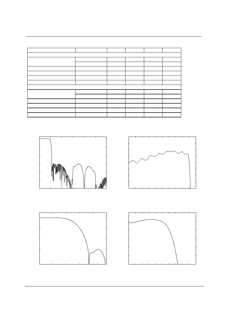
Production Data
WM8770
w
PD Rev 4.1 June 2005
45
DIGITAL FILTER CHARACTERISTICS
PARAMETER TEST
CONDITIONS
MIN
TYP
MAX
UNIT
ADC Filter
±
0.01 dB
0
0.4535fs
Passband
-6dB
0.5fs
Passband ripple
±
0.01 dB
Stopband
0.5465fs
Stopband Attenuation
f > 0.5465fs
-65
dB
Group Delay
22
fs
DAC Filter
±
0.05 dB
0.444fs
Passband
-3dB
0.487fs
Passband ripple
±
0.05 dB
Stopband
0.555fs
Stopband Attenuation
f > 0.555fs
-60
dB
Group Delay
16
fs
Table 16 Digital Filter Characteristics
DAC FILTER RESPONSES
-120
-100
-80
-60
-40
-20
0
0
0.5
1
1.5
2
2.5
3
Response (dB)
Frequency (Fs)
Figure 27 DAC Digital Filter Frequency Response
≠ 44.1, 48 and 96kHz
-0.2
-0.15
-0.1
-0.05
0
0.05
0.1
0.15
0.2
0
0.05
0.1
0.15
0.2
0.25
0.3
0.35
0.4
0.45
0.5
Response (dB)
Frequency (Fs)
Figure 28 DAC Digital Filter Ripple ≠ 44.1, 48 and 96kHz
-80
-60
-40
-20
0
0
0.2
0.4
0.6
0.8
1
Response (dB)
Frequency (Fs)
Figure 29 DAC Digital Filter Frequency Response ≠ 192kHz
-1
-0.8
-0.6
-0.4
-0.2
0
0.2
0
0.05
0.1
0.15
0.2
0.25
0.3
0.35
0.4
0.45
0.5
Response (dB)
Frequency (Fs)
Figure 30 DAC Digital filter Ripple - 192kHz

WM8770
Production Data
w
PD Rev 4.1 June 2005
46
ADC FILTER RESPONSES
-80
-60
-40
-20
0
0
0.5
1
1.5
2
2.5
3
Response (dB)
Frequency (Fs)
Figure 31 ADC Digital Filter Frequency Response
-0.02
-0.015
-0.01
-0.005
0
0.005
0.01
0.015
0.02
0
0.05
0.1
0.15
0.2
0.25
0.3
0.35
0.4
0.45
0.5
Response (dB)
Frequency (Fs)
Figure 32 ADC Digital Filter Ripple
ADC HIGH PASS FILTER
The WM8770 has a selectable digital highpass filter to remove DC offsets. The filter response is characterised by the
following polynomial.
Figure 33 ADC Highpass Filter Response
1 - z
-1
1 - 0.9995z
-1
H(z) =
-15
-10
-5
0
0
0.0005
0.001
0.0015
0.002
Response (dB)
Frequency (Fs)
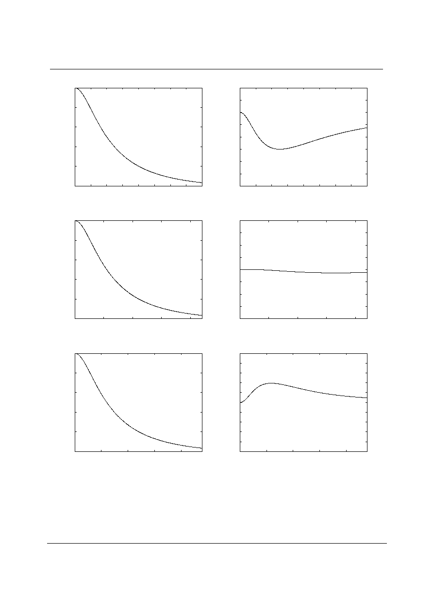
Production Data
WM8770
w
PD Rev 4.1 June 2005
47
DIGITAL DE-EMPHASIS CHARACTERISTICS
-10
-8
-6
-4
-2
0
0
2
4
6
8
10
12
14
16
Response (dB)
Frequency (kHz)
Figure 34 De-Emphasis Frequency Response (32kHz)
-3
-2.5
-2
-1.5
-1
-0.5
0
0.5
1
0
2
4
6
8
10
12
14
16
Response (dB)
Frequency (kHz)
Figure 35 De-Emphasis Error (32KHz)
-10
-8
-6
-4
-2
0
0
5
10
15
20
Response (dB)
Frequency (kHz)
Figure 36 De-Emphasis Frequency Response (44.1KHz)
-0.4
-0.3
-0.2
-0.1
0
0.1
0.2
0.3
0.4
0
5
10
15
20
Response (dB)
Frequency (kHz)
Figure 37 De-Emphasis Error (44.1KHz)
-10
-8
-6
-4
-2
0
0
5
10
15
20
Response (dB)
Frequency (kHz)
Figure 38 De-Emphasis Frequency Response (48kHz)
-1
-0.8
-0.6
-0.4
-0.2
0
0.2
0.4
0.6
0.8
1
0
5
10
15
20
Response (dB)
Frequency (kHz)
Figure 39 De-Emphasis Error (48kHz)
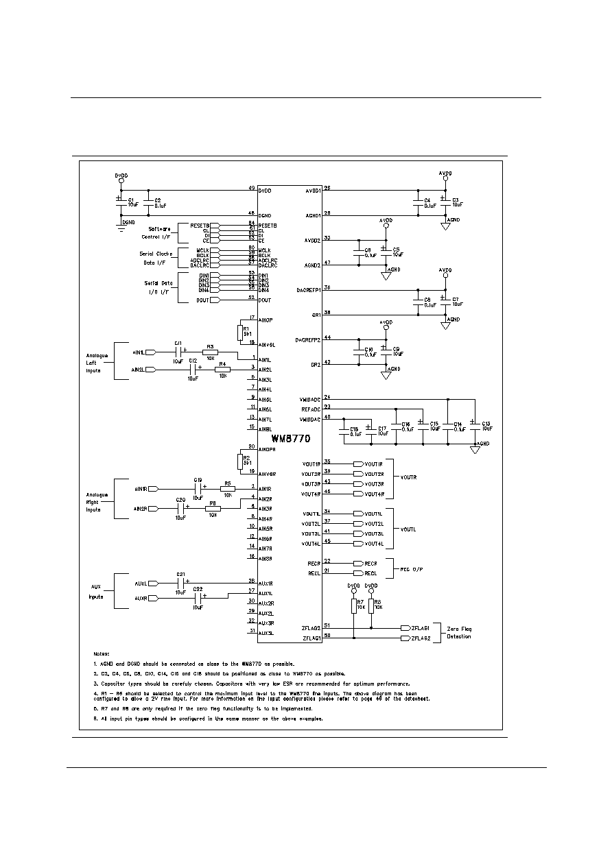
WM8770
Production Data
w
PD Rev 4.1 June 2005
48
APPLICATIONS INFORMATION
RECOMMENDED EXTERNAL COMPONENTS
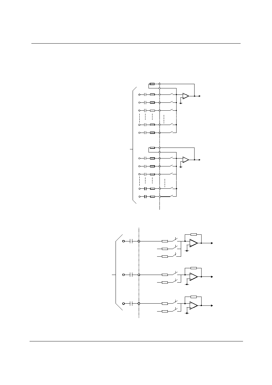
Production Data
WM8770
w
PD Rev 4.1 June 2005
49
AIN1L
10K
10uF
AIN2L
10K
10uF
AIN3L
10K
10uF
AIN7L
10K
10uF
AIN8L
10K
10uF
AIN1R
10K
10uF
AIN2R
10K
10uF
AIN3R
10K
10uF
AIN7R
10K
10uF
AIN8R
10K
10uF
SOURCE
SELECTOR
INPUTS
AINVGR
AINOPR
5K
AINVGL
AINOPL
5K
EXTERNAL CIRCUIT CONFIGURATION
In order to allow the use of 2V rms and larger inputs to the ADC and AUX inputs, a structure is used
that uses external resistors to drop these larger voltages. This also increases the robustness of the
circuit to external abuse such as ESD pulse.
Figure 40 shows the ADC input multiplexor circuit with external components allowing 2Vrms inputs to
be applied.
Figure 40 ADC Input Multiplexor Configuration
Figure 41 Shows the 5.1Channel Input Multiplexor Configuration
SYSTEM
AUX 5.1
LINE INPUTS
4K
MX1[1]
MX1[0]
MX1[2]
4K
4K
4K
DAC1L/R
BYPASSL/R
AUX1L/R
4K
MX2[1]
MX2[0]
4K
4K
DAC2L/R
DAC3L/R
10uF
10uF
AUX2L/R
10uF
AUX3L/R
4K
MX3[1]
MX3[0]
4K
4K

WM8770
Production Data
w
PD Rev 4.1 June 2005
50
It is recommended that a lowpass filter be applied to the output from each DAC channel for Hi Fi
applications. Typically a second order filter is suitable and provides sufficient attenuation of high
frequency components (the unique low order, high bit count multi-bit sigma delta DAC structure used
in WM8770 produces much less high frequency output noise than competitors devices). This filter is
typically also used to provide the 2x gain needed to provide the standard 2Vrms output level from
most consumer equipment. Figure 24 shows a suitable post DAC filter circuit, with 2x gain.
Alternative inverting filter architectures might also be used with as good results.
Figure 41 Recommended Post DAC Filter Circuit
7.5k
1.8k
10uF
1.0nF
47k
4.7k
680pF
4.7k
51
OP_FIL
VOUT1L
OP_FIL
VOUT1R
OP_FIL
VOUT2R
OP_FIL
VOUT2L
OP_FIL
VOUT3L
OP_FIL
VOUT3R
OP_FIL
VOUT4L
OP_FIL
VOUT4R
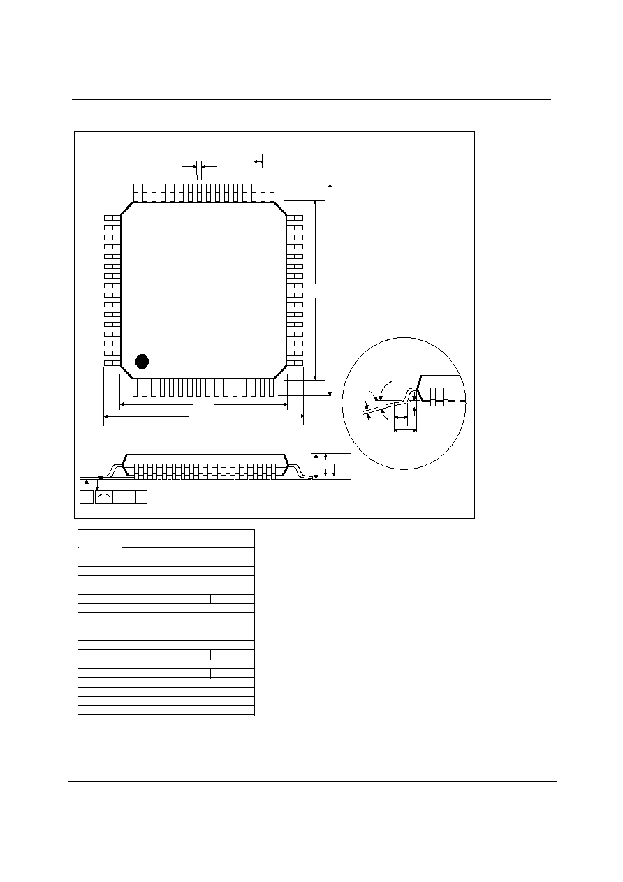
Production Data
WM8770
w
PD Rev 4.1 June 2005
51
PACKAGE DIMENSIONS
DM027.B
FT: 64 PIN TQFP (10 x 10 x 1.0 mm)
e
33
b
16
D1
17
64
49
48
D
1
32
E1
E
GAUGE
PLANE
L
0.25
L
1
c
SEATING
PLANE
A2
A1
NOTES:
A. ALL LINEAR DIMENSIONS ARE IN MILLIMETERS.
B. THIS DRAWING IS SUBJECT TO CHANGE WITHOUT NOTICE.
C. BODY DIMENSIONS DO NOT INCLUDE MOLD FLASH OR PROTRUSION, NOT TO EXCEED 0.25MM.
D. MEETS JEDEC.95 MS-026, VARIATION = ACD. REFER TO THIS SPECIFICATION FOR FURTHER DETAILS.
0
o
3.5
o
7
o
Tolerances of Form and Position
ccc
0.08
REF:
JEDEC.95, MS-026, VARIATION ACD
Symbols
Dimensions
(mm)
MIN
NOM
MAX
A
-----
-----
1.20
A
1
0.05
-----
0.15
A
2
1.00
b
0.22
c
-----
0.20
D
12.00 BSC
D
1
10.00 BSC
E
12.00 BSC
10.00 BSC
e
0.50 BSC
L
0.60
0.95
0.17
0.09
0.27
1.05
0.45
0.75
1.00 REF
A
-C-
E
1
L
1
ccc
C

WM8770
Production Data
w
PD Rev 4.1 June 2005
52
IMPORTANT NOTICE
Wolfson Microelectronics plc (WM) reserve the right to make changes to their products or to discontinue any product or
service without notice, and advise customers to obtain the latest version of relevant information to verify, before placing
orders, that information being relied on is current. All products are sold subject to the WM terms and conditions of sale
supplied at the time of order acknowledgement, including those pertaining to warranty, patent infringement, and limitation
of liability.
WM warrants performance of its products to the specifications applicable at the time of sale in accordance with WM's
standard warranty. Testing and other quality control techniques are utilised to the extent WM deems necessary to support
this warranty. Specific testing of all parameters of each device is not necessarily performed, except those mandated by
government requirements.
In order to minimise risks associated with customer applications, adequate design and operating safeguards must be used
by the customer to minimise inherent or procedural hazards. Wolfson products are not authorised for use as critical
components in life support devices or systems without the express written approval of an officer of the company. Life
support devices or systems are devices or systems that are intended for surgical implant into the body, or support or
sustain life, and whose failure to perform when properly used in accordance with instructions for use provided, can be
reasonably expected to result in a significant injury to the user. A critical component is any component of a life support
device or system whose failure to perform can be reasonably expected to cause the failure of the life support device or
system, or to affect its safety or effectiveness.
WM assumes no liability for applications assistance or customer product design. WM does not warrant or represent that
any license, either express or implied, is granted under any patent right, copyright, mask work right, or other intellectual
property right of WM covering or relating to any combination, machine, or process in which such products or services might
be or are used. WM's publication of information regarding any third party's products or services does not constitute WM's
approval, license, warranty or endorsement thereof.
Reproduction of information from the WM web site or datasheets is permissible only if reproduction is without alteration and
is accompanied by all associated warranties, conditions, limitations and notices. Representation or reproduction of this
information with alteration voids all warranties provided for an associated WM product or service, is an unfair and deceptive
business practice, and WM is not responsible nor liable for any such use.
Resale of WM's products or services with statements different from or beyond the parameters stated by WM for that
product or service voids all express and any implied warranties for the associated WM product or service, is an unfair and
deceptive business practice, and WM is not responsible nor liable for any such use.
ADDRESS:
Wolfson Microelectronics plc
26 Westfield Road
Edinburgh
EH11 2QB
United Kingdom
Tel :: +44 (0)131 272 7000
Fax :: +44 (0)131 272 7001
Email ::
sales@wolfsonmicro.com