Document Outline
- WM8971L
- Stereo CODEC for Portable Audio Applications
- DESCRIPTION
- FEATURES
- APPLICATIONS
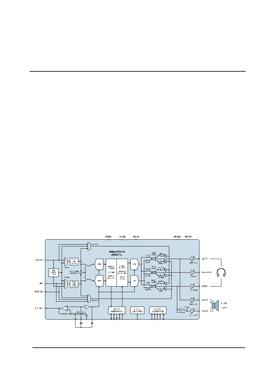
- BLOCK DIAGRAM
- TABLE OF CONTENTS
- PIN CONFIGURATION
- ORDERING INFORMATION
- PIN DESCRIPTION
- ABSOLUTE MAXIMUM RATINGS
- RECOMMENDED OPERATION CONDITIONS
- ELECTRICAL CHARACTERISTICS
- OUTPUT PGAêS LINEARITY
- HEADPHONE OUTPUT THD VERSUS POWER
- SPEAKER OUTPUT THD VERSUS POWER
- POWER CONSUMPTION
- SIGNAL TIMING REQUIREMENTS
- SYSTEM CLOCK TIMING
- AUDIO INTERFACE TIMING Ö MASTER MODE
- AUDIO INTERFACE TIMING Ö SLAVE MODE
- DEVICE DESCRIPTION
- INTRODUCTION
- INPUT SIGNAL PATH
- AUTOMATIC LEVEL CONTROL (ALC)
- OUTPUT SIGNAL PATH
- ANALOGUE OUTPUTS
- ENABLING THE OUTPUTS
- HEADPHONE SWITCH
- THERMAL SHUTDOWN
- HEADPHONE OUTPUT
- DIGITAL AUDIO INTERFACE
- AUDIO INTERFACE CONTROL
- CLOCKING AND SAMPLE RATES
- CONTROL INTERFACE
- POWER SUPPLIES
- POWER MANAGEMENT
- REGISTER MAP
- DIGITAL FILTER CHARACTERISTICS
- TERMINOLOGY
- DAC FILTER RESPONSES
- ADC FILTER RESPONSES
- DE-EMPHASIS FILTER RESPONSES
- HIGHPASS FILTER
- APPLICATIONS INFORMATION
- RECOMMENDED EXTERNAL COMPONENTS
- LINE INPUT CONFIGURATION
- MICROPHONE INPUT CONFIGURATION
- MINIMISING POP NOISE AT THE ANALOGUE OUTPUTS
- POWER MANAGEMENT EXAMPLES
- PACKAGE DIMENSIONS
- IMPORTANT NOTICE
w
WM8971L
Stereo CODEC for Portable Audio Applications
WOLFSON MICROELECTRONICS plc
www.wolfsonmicro.com
Advanced Information, March 2004, Rev 3.0
Copyright
2004 Wolfson Microelectronics plc
DESCRIPTION
The WM8971L is a low power, high quality stereo codec
designed for portable digital audio applications.
The device integrates complete interfaces to stereo or mono
microphones and a stereo headphone. External component
requirements are drastically reduced as no separate
microphone or headphone amplifiers are required.
Advanced on-chip digital signal processing performs
graphic equaliser, and automatic level control for the
microphone or line input.
The WM8971L can operate as a master or a slave, with
various master clock frequencies including 12 or 24MHz for
USB devices, or standard 256f
s
rates like 12.288MHz and
24.576MHz. Different audio sample rates such as 96kHz,
48kHz, 44.1kHz are generated directly from the master
clock without the need for an external PLL.
The WM8971L operates at supply voltages down to 1.8V,
although the digital core can operate at voltages down to
1.42V to save power, and the maximum for all supplies is
3.6 Volts. Different sections of the chip can also be powered
down under software control.
The WM8971L is supplied in a very small and thin 5x5mm
QFN package, ideal for use in hand-held and portable
systems.
FEATURES
∑
DAC SNR 98dB (`A' weighted), THD ≠84dB at 48kHz, 3.3V
∑
ADC SNR 95dB (`A' weighted), THD -82dB at 48kHz, 3.3V
∑
Complete Stereo / Mono Microphone Interface
- Programmable ALC / Noise Gate
∑
On-chip 400mW BTL Speaker Driver (mono)
∑
On-chip
Headphone
Driver
-
>40mW output power on 16
/ 3.3V
-
THD ≠80dB at 20mW, SNR 90dB with 16
load
-
No DC blocking capacitors required (capless mode)
∑
Separately mixed mono output
∑
Digital Graphic Equaliser
∑
Low
Power
-
7mW stereo playback (1.8V / 1.5V supplies)
-
14mW record and playback (1.8V / 1.5V supplies)
∑
Low Supply Voltages
-
Analogue 1.8V to 3.6V
-
Digital core: 1.42V to 3.6V
-
Digital I/O: 1.8V to 3.6V
∑
256fs / 384fs or USB master clock rates: 12MHz, 24MHz
∑
Audio sample rates: 8, 11.025, 16, 22.05, 24, 32, 44.1, 48,
88.2, 96kHz generated internally from master clock
∑
5x5x0.9mm QFN package
APPLICATIONS
∑
Digital
Still
Cameras
∑
MP3 Player / Recorders
∑
Minidisc Player / Recorders
∑
Portable Digital Music Systems
BLOCK DIAGRAM
CSB
SD
I
N
SCLK
MODE
VR
EF
AVD
D
AGND
VM
ID
AD
CDAT
AD
CLR
C
BCLK
MCL
K
DA
CDAT
DA
CL
R
C
HPDE
TECT

WM8971L
Advanced Information
w
AI Rev 3.0 March 2004
2
TABLE OF CONTENTS
DESCRIPTION .......................................................................................................1
FEATURES.............................................................................................................1
APPLICATIONS .....................................................................................................1
BLOCK DIAGRAM .................................................................................................1
TABLE OF CONTENTS .........................................................................................2
PIN CONFIGURATION...........................................................................................4
ORDERING INFORMATION ..................................................................................4
PIN DESCRIPTION ................................................................................................5
ABSOLUTE MAXIMUM RATINGS .........................................................................6
RECOMMENDED OPERATION CONDITIONS .....................................................6
ELECTRICAL CHARACTERISTICS ......................................................................7
OUTPUT PGA'S LINEARITY ......................................................................................... 9
HEADPHONE OUTPUT THD VERSUS POWER......................................................... 10
SPEAKER OUTPUT THD VERSUS POWER .............................................................. 11
POWER CONSUMPTION ....................................................................................12
SIGNAL TIMING REQUIREMENTS .....................................................................13
SYSTEM CLOCK TIMING............................................................................................ 13
AUDIO INTERFACE TIMING ≠ MASTER MODE ......................................................... 13
AUDIO INTERFACE TIMING ≠ SLAVE MODE ............................................................ 14
DEVICE DESCRIPTION .......................................................................................17
INTRODUCTION.......................................................................................................... 17
INPUT SIGNAL PATH.................................................................................................. 17
AUTOMATIC LEVEL CONTROL (ALC) ....................................................................... 23
OUTPUT SIGNAL PATH.............................................................................................. 26
ANALOGUE OUTPUTS ............................................................................................... 31
ENABLING THE OUTPUTS ......................................................................................... 33
HEADPHONE SWITCH ............................................................................................... 33
THERMAL SHUTDOWN .............................................................................................. 35
HEADPHONE OUTPUT ............................................................................................... 35
DIGITAL AUDIO INTERFACE...................................................................................... 36
AUDIO INTERFACE CONTROL .................................................................................. 39
CLOCKING AND SAMPLE RATES .............................................................................. 40
CONTROL INTERFACE .............................................................................................. 42
POWER SUPPLIES ..................................................................................................... 43
POWER MANAGEMENT ............................................................................................. 44
REGISTER MAP...................................................................................................46
DIGITAL FILTER CHARACTERISTICS ...............................................................47
TERMINOLOGY........................................................................................................... 47
DAC FILTER RESPONSES ......................................................................................... 48
ADC FILTER RESPONSES ......................................................................................... 49
DE-EMPHASIS FILTER RESPONSES ........................................................................ 50
HIGHPASS FILTER ..................................................................................................... 51

Advanced Information
WM8971L
w
AI Rev 3.0 March 2004
3
APPLICATIONS INFORMATION .........................................................................52
RECOMMENDED EXTERNAL COMPONENTS........................................................... 52
LINE INPUT CONFIGURATION................................................................................... 53
MICROPHONE INPUT CONFIGURATION .................................................................. 53
MINIMISING POP NOISE AT THE ANALOGUE OUTPUTS ........................................ 54
POWER MANAGEMENT EXAMPLES ......................................................................... 54
IMPORTANT NOTICE ..........................................................................................56
ADDRESS:................................................................................................................... 56

WM8971L
Advanced Information
w
AI Rev 3.0 March 2004
4
PIN CONFIGURATION
ORDERING INFORMATION
ORDER CODE
TEMPERATURE RANGE
PACKAGE
MOISTURE
SENSITIVITY LEVEL
PEAK SOLDERING
TEMPERATURE
WM8971LEFL -25
∞
C to +85
∞
C 32-pin
QFN
(5x5x0.9mm) MSL1 260∞C
WM8971LEFL/R -25
∞
C to +85
∞
C 32-pin
QFN
(5x5x0.9mm)
(tape and reel)
MSL1 260∞C
WM8971LGEFL -25
∞
C to +85
∞
C 32-pin
QFN
(5x5x0.9mm)
(lead free)
MSL1 260∞C
WM8971LGEFL/R -25
∞
C to +85
∞
C 32-pin
QFN
(5x5x0.9mm)
(lead free, tape and reel)
MSL1 260∞C
Note:
Reel quantity = 3500
Advanced Information
WM8971L
w
AI Rev 3.0 March 2004
5
PIN DESCRIPTION
PIN NO
NAME
TYPE
DESCRIPTION
1 MCLK
Digital Input
Master Clock
2 DCVDD
Supply Digital
Core
Supply
3 DBVDD
Supply
Digital Buffer (I/O) Supply
4 DGND
Supply
Digital Ground (return path for both DCVDD and DBVDD)
5 BCLK
Digital Input / Output
Audio Interface Bit Clock
6 DACDAT
Digital Input
DAC Digital Audio Data
7 DACLRC
Digital Input / Output
Audio Interface Left / Right Clock/Clock Out
8 ADCDAT
Digital Output
ADC Digital Audio Data
9 ADCLRC
Digital Input / Output
Audio Interface Left / Right Clock
10 MONOOUT
Analogue Output
Mono Output
11 NC
No Connect
No Connect
12 ROUT1
Analogue Output
Right Output 1 (Line or Headphone)
13 LOUT1
Analogue Output
Left Output 1 (Line or Headphone)
14 HPGND
Supply
Supply for Analogue Output Drivers (LOUT1/2, ROUT1/2)
15 ROUT2
Analogue Output
Right Output 1 (Line or Headphone or Speaker)
16 LOUT2
Analogue Output
Left Output 1 (Line or Headphone or Speaker)
17 HPVDD
Supply
Supply for Analogue Output Drivers (LOUT1/2, ROUT1/2,
MONOUT)
18 AVDD
Supply Analogue
Supply
19 AGND
Supply
Analogue Ground (return path for both AVDD and MVDD)
20 VREF
Analogue Output
Reference Voltage Decoupling Capacitor
21 VMID
Analogue Output
Midrail Voltage Decoupling Capacitor
22 MICBIAS
Analogue Output
Microphone Bias
23 HPDETECT
Analogue Input
Headphone Plug-in Detection
24 NC
No Connect
No Connect
25 MIC
Analogue Input
Single Ended Microphone Input
26 NC
No Connect
No Connect
27 RINPUT1
Analogue Input
Right Channel Input 1
28 LINPUT1
Analogue Input
Left Channel Input 1
29 MODE
Digital Input
Control Interface Selection
30 CSB
Digital Input
Chip Select / Device Address Selection
31 SDIN
Digital Input/Output
Control Interface Data Input / 2-wire Acknowledge output
32
SCLK
Digital Input
Control Interface Clock Input