Document Outline
- WM8972L
- Mono CODEC for Portable Audio Applications
- DESCRIPTION
- FEATURES
- APPLICATIONS
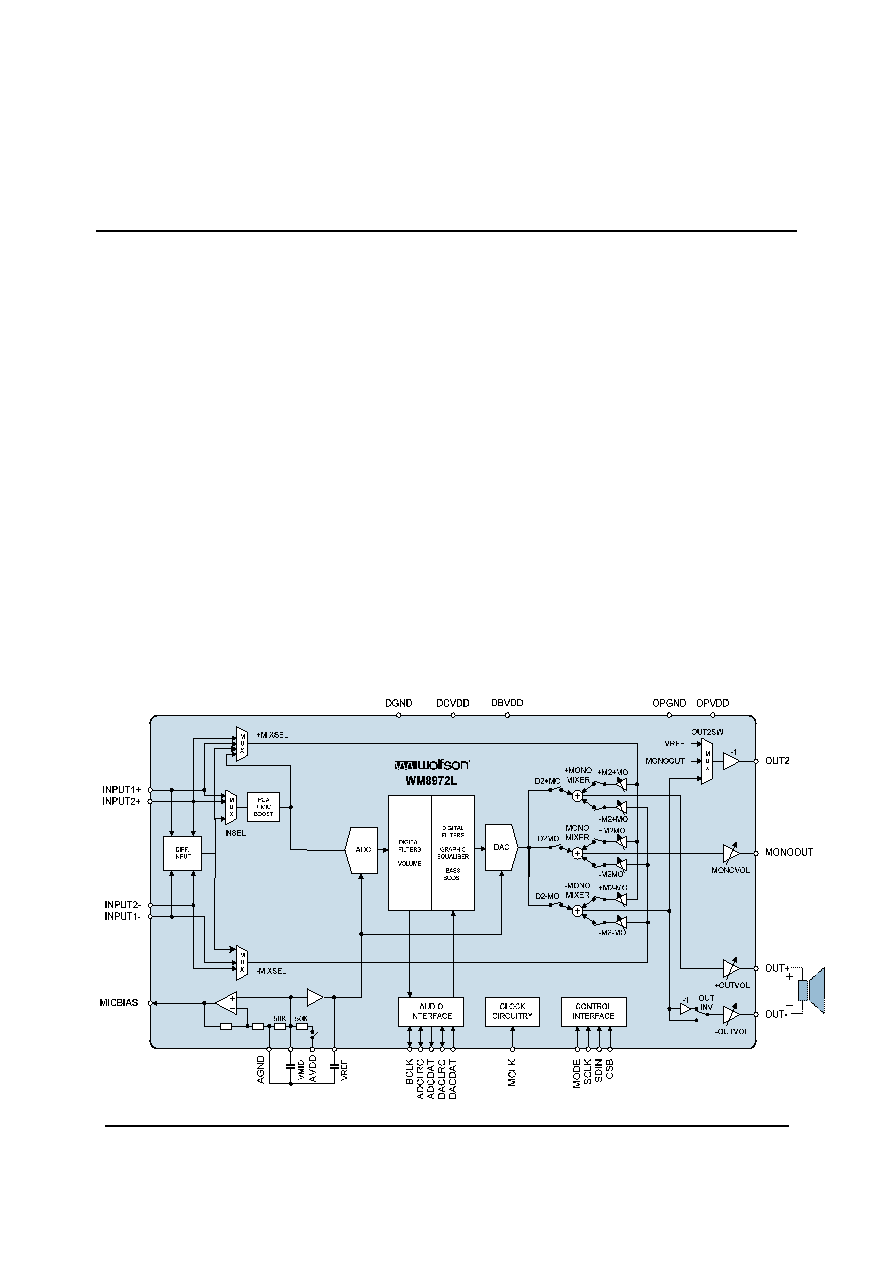
- BLOCK DIAGRAM
- TABLE OF CONTENTS
- PIN CONFIGURATION
- ORDERING INFORMATION
- PIN DESCRIPTION
- ABSOLUTE MAXIMUM RATINGS
- RECOMMENDED OPERATION CONDITIONS
- ELECTRICAL CHARACTERISTICS
- OUTPUT PGA ê S LINEARITY
- POWER CONSUMPTION
- SIGNAL TIMING REQUIREMENTS
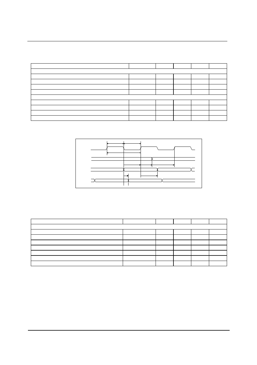
- SYSTEM CLOCK TIMING
- AUDIO INTERFACE TIMING Ö MASTER MODE
- AUDIO INTERFACE TIMING Ö SLAVE MODE
- DEVICE DESCRIPTION
- INTRODUCTION
- INPUT SIGNAL PATH
- AUTOMATIC LEVEL CONTROL (ALC)
- OUTPUT SIGNAL PATH
- ANALOGUE OUTPUTS
- ENABLING THE OUTPUTS
- THERMAL SHUTDOWN
- DIGITAL AUDIO INTERFACE
- AUDIO INTERFACE CONTROL
- CLOCKING AND SAMPLE RATES
- CONTROL INTERFACE
- POWER SUPPLIES
- POWER MANAGEMENT
- REGISTER MAP
- DIGITAL FILTER CHARACTERISTICS
- TERMINOLOGY
- DAC FILTER RESPONSES
- ADC FILTER RESPONSES
- DE-EMPHASIS FILTER RESPONSES
- HIGHPASS FILTER
- APPLICATIONS INFORMATION
- RECOMMENDED EXTERNAL COMPONENTS
- LINE INPUT CONFIGURATION
- MICROPHONE INPUT CONFIGURATION
- POWER MANAGEMENT EXAMPLES
- PACKAGE DIMENSIONS
- IMPORTANT NOTICE
w
WM8972L
Mono CODEC for Portable Audio Applications
WOLFSON MICROELECTRONICS plc
www.wolfsonmicro.com
Preliminary Technical Data, June 2004, Rev 2.2
Copyright
2004 Wolfson Microelectronics plc
DESCRIPTION
The WM8972L is a low power, high quality mono CODEC
designed for portable digital audio applications.
The device integrates complete interfaces to mono
microphones.
External component requirements are
drastically reduced as no separate microphone amplifiers
are required. Advanced on-chip digital signal processing
performs graphic equaliser and automatic level control for
the microphone or line input.
The WM8972L can operate as a master or a slave, with
various master clock frequencies including 12 or 24MHz for
USB devices, or standard 256f
s
rates like 12.288MHz and
24.576MHz. Different audio sample rates such as 96kHz,
48kHz, 44.1kHz are generated directly from the master
clock without the need for an external PLL.
The WM8972L operates at supply voltages down to 1.8V,
although the digital core can operate at voltages down to
1.42V to save power, and the maximum for all supplies is
3.6 Volts. Different sections of the chip can also be powered
down under software control.
The WM8972L is supplied in a very small and thin 5x5mm
QFN package, ideal for use in hand-held and portable
systems.
FEATURES
∑ DAC SNR 98dB (`A' weighted), THD ≠84dB at 48kHz, 3.3V
∑ ADC SNR 95dB (`A' weighted), THD -82dB at 48kHz, 3.3V
∑ Complete Mono Microphone Interface
- Programmable ALC / Noise Gate
∑ On-chip 400mW BTL Speaker Driver (mono)
∑ Digital Graphic Equaliser
∑ Low Power
-
7mW mono playback (1.8V / 1.5V supplies)
-
14mW record & playback (1.8V / 1.5V supplies)
∑ Low Supply Voltages
-
Analogue 1.8V to 3.6V
-
Digital core: 1.42V to 3.6V
-
Digital I/O: 1.8V to 3.6V
∑ 256fs / 384fs or USB master clock rates: 12MHz, 24MHz
∑ Audio sample rates: 8, 11.025, 16, 22.05, 24, 32, 44.1, 48,
88.2, 96kHz generated internally from master clock
∑ 5x5x0.9mm QFN package
APPLICATIONS
∑ Digital Still Cameras
∑ Toys
BLOCK DIAGRAM

WM8972L
Preliminary Technical Data
w
PTD Rev 2.2 June 2004
2
TABLE OF CONTENTS
DESCRIPTION.......................................................................................................1
FEATURES.............................................................................................................1
APPLICATIONS .....................................................................................................1
BLOCK DIAGRAM .................................................................................................1
TABLE OF CONTENTS .........................................................................................2
PIN CONFIGURATION...........................................................................................3
ORDERING INFORMATION ..................................................................................3
PIN DESCRIPTION ................................................................................................4
ABSOLUTE MAXIMUM RATINGS .........................................................................5
RECOMMENDED OPERATION CONDITIONS .....................................................5
ELECTRICAL CHARACTERISTICS ......................................................................6
OUTPUT PGA'S LINEARITY ......................................................................................... 7
POWER CONSUMPTION ......................................................................................8
SIGNAL TIMING REQUIREMENTS .......................................................................9
SYSTEM CLOCK TIMING.............................................................................................. 9
AUDIO INTERFACE TIMING ≠ MASTER MODE ........................................................... 9
AUDIO INTERFACE TIMING ≠ SLAVE MODE ............................................................ 10
DEVICE DESCRIPTION.......................................................................................13
INTRODUCTION.......................................................................................................... 13
INPUT SIGNAL PATH.................................................................................................. 13
AUTOMATIC LEVEL CONTROL (ALC) ....................................................................... 18
OUTPUT SIGNAL PATH.............................................................................................. 21
ANALOGUE OUTPUTS ............................................................................................... 26
ENABLING THE OUTPUTS ......................................................................................... 27
THERMAL SHUTDOWN .............................................................................................. 27
DIGITAL AUDIO INTERFACE...................................................................................... 28
AUDIO INTERFACE CONTROL .................................................................................. 31
CLOCKING AND SAMPLE RATES .............................................................................. 32
CONTROL INTERFACE .............................................................................................. 34
POWER SUPPLIES ..................................................................................................... 35
POWER MANAGEMENT ............................................................................................. 36
REGISTER MAP .......................................................................................................... 38
DIGITAL FILTER CHARACTERISTICS ...............................................................39
TERMINOLOGY........................................................................................................... 39
DAC FILTER RESPONSES ......................................................................................... 40
ADC FILTER RESPONSES ......................................................................................... 41
DE-EMPHASIS FILTER RESPONSES ........................................................................ 42
HIGHPASS FILTER ..................................................................................................... 43
APPLICATIONS INFORMATION .........................................................................44
RECOMMENDED EXTERNAL COMPONENTS........................................................... 44
LINE INPUT CONFIGURATION................................................................................... 45
MICROPHONE INPUT CONFIGURATION .................................................................. 45
MINIMISING POP NOISE AT THE ANALOGUE OUTPUTS ........................................ 46
POWER MANAGEMENT EXAMPLES ......................................................................... 46
IMPORTANT NOTICE ..........................................................................................48
ADDRESS:................................................................................................................... 48
Preliminary Technical Data
WM8972L
w
PTD Rev 2.2 June 2004
3
PIN CONFIGURATION
1
2
3
4
5
6
7
8
24
23
22
21
20
19
18
17
16
15
14
13
12
11
10
9
25
26
27
28
29
30
31
32
DA
CD
A
T
BC
L
K
DC
V
D
D
DG
N
D
DB
V
D
D
MCL
K
DA
CL
RC
OUT2
AV
D
D
VM
I
D
AG
N
D
VR
EF
MI
CB
I
A
S
DN
C
OPGND
ADCLRC
MONOOUT
OP
V
D
D
DNC
DNC
OUT-
OUT+
AD
C
D
AT
CSB
MODE
INPUT2+
INPUT1+
INPUT1-
INPUT2-
DN
C
SDIN
SCLK
ORDERING INFORMATION
ORDER CODE
TEMPERATURE
RANGE
PACKAGE
MOISTURE SENSITIVITY
LEVEL
PEAK SOLDERING
TEMPERATURE
WM8972LEFL
-25
∞C to +85∞C
32-pin QFN (5x5x0.9mm)
MSL1
260
o
C
WM8972LEFL/R
-25
∞C to +85∞C
32-pin QFN (5x5x0.9mm)
(tape and reel)
MSL1
260
o
C
WM8972LGEFL
-25
∞C to +85∞C
32-pin QFN (5x5x0.9mm)
(lead free)
MSL1
260
o
C
WM8972LGEFL/R
-25
∞C to +85∞C
32-pin QFN (5x5x0.9mm)
(lead free, tape and reel)
MSL1
260
o
C
Note:
Reel quantity = 3,500
WM8972L
Preliminary Technical Data
w
PTD Rev 2.2 June 2004
4
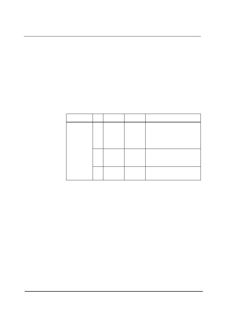
PIN DESCRIPTION
PIN NO
NAME
TYPE
DESCRIPTION
1
MCLK
Digital Input
Master Clock
2
DCVDD
Supply
Digital Core Supply
3
DBVDD
Supply
Digital Buffer (I/O) Supply
4
DGND
Supply
Digital Ground (return path for both DCVDD and DBVDD)
5
BCLK
Digital Input / Output
Audio Interface Bit Clock
6
DACDAT
Digital Input
DAC Digital Audio Data
7
DACLRC
Digital Input / Output
Audio Interface Left / Right Clock/Clock Out
8
ADCDAT
Digital Output
ADC Digital Audio Data
9
ADCLRC
Digital Input / Output
Audio Interface Left / Right Clock
10
MONOOUT
Analogue Output
Mono Output
11
OUT2
Analogue Output
Analogue Output 2
12
DNC
Do not connect
Leave this pin floating
13
DNC
Do not connect
Leave this pin floating
14
OPGND
Supply
Supply for Analogue Output Drivers
15
OUT-
Analogue Output
- Output (Line or Speaker)
16
OUT+
Analogue Output
+ Output (Line or Speaker)
17
OPVDD
Supply
Supply for Analogue Output Drivers (OUT-/+, MONOUT)
18
AVDD
Supply
Analogue Supply
19
AGND
Supply
Analogue Ground (return path for both AVDD and MVDD)
20
VREF
Analogue Output
Reference Voltage Decoupling Capacitor
21
VMID
Analogue Output
Midrail Voltage Decoupling Capacitor
22
MICBIAS
Analogue Output
Microphone Bias
23
DNC
Do not connect
Leave this pin floating
24
DNC
Do not connect
Leave this pin floating
25
INPUT2-
Analogue Input
- Channel Input 2
26
INPUT2+
Analogue Input
+ Channel Input 2
27
INPUT1-
Analogue Input
- Channel Input 1
28
INPUT1+
Analogue Input
+ Channel Input 1
29
MODE
Digital Input
Control Interface Selection
30
CSB
Digital Input
Chip Select / Device Address Selection
31
SDIN
Digital Input/Output
Control Interface Data Input / 2-wire Acknowledge output
32
SCLK
Digital Input
Control Interface Clock Input
Preliminary Technical Data
WM8972L
w
PTD Rev 2.2 June 2004
5
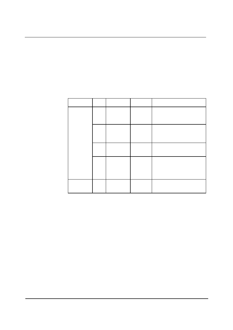
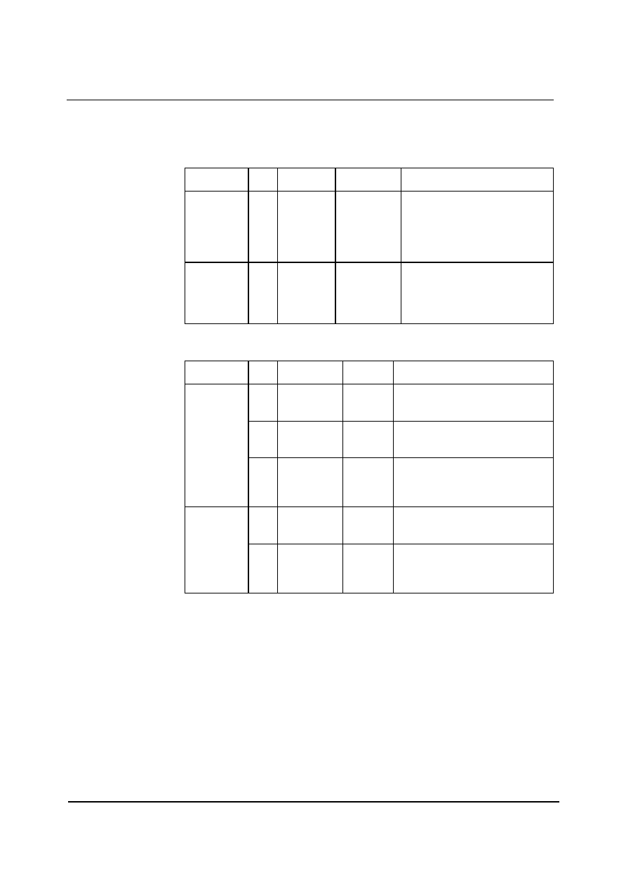
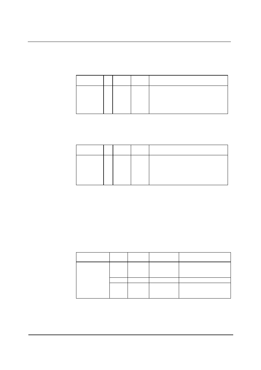
ABSOLUTE MAXIMUM RATINGS
Absolute Maximum Ratings are stress ratings only. Permanent damage to the device may be caused by continuously
operating at or beyond these limits. Device functional operating limits and guaranteed performance specifications are given
under Electrical Characteristics at the test conditions specified.
ESD Sensitive Device. This device is manufactured on a CMOS process. It is therefore generically susceptible
to damage from excessive static voltages. Proper ESD precautions must be taken during handling and storage
of this device.
Wolfson tests its package types according to IPC/JEDEC J-STD-020B for Moisture Sensitivity to determine acceptable storage
conditions prior to surface mount assembly. These levels are:
MSL1 = unlimited floor life at <30
∞C / 85% Relative Humidity. Not normally stored in moisture barrier bag.
MSL2 = out of bag storage for 1 year at <30
∞C / 60% Relative Humidity. Supplied in moisture barrier bag.
MSL3 = out of bag storage for 168 hours at <30
∞C / 60% Relative Humidity. Supplied in moisture barrier bag.
The Moisture Sensitivity Level for each package type is specified in Ordering Information.
CONDITION
MIN
MAX
Supply voltages
-0.3V
+3.63V
Voltage range digital inputs
DGND -0.3V
DBVDD +0.3V
Voltage range analogue inputs
AGND -0.3V
AVDD +0.3V
Operating temperature range, T
A
-25
∞C
+85
∞C
Storage temperature after soldering
-65
∞C
+150
∞C
Notes
1.
Analogue and digital grounds must always be within 0.3V of each other.
2.
All digital and analogue supplies are completely independent from each other.
3.
DCVDD must be less than or equal to AVDD & DBVDD.
RECOMMENDED OPERATION CONDITIONS
PARAMETER
SYMBOL
MIN
TYP
MAX
UNIT
Digital supply range (Core)
DCVDD
1.42
2.0
3.6
V
Digital supply range (Buffer)
DBVDD
1.8
2.0
3.6
V
Analogue supplies range
AVDD, OPVDD
1.8
2.0
3.6
V
Ground
DGND,AGND, OPGND
0
V
WM8972L
Preliminary Technical Data
w
PTD Rev 2.2 June 2004
6
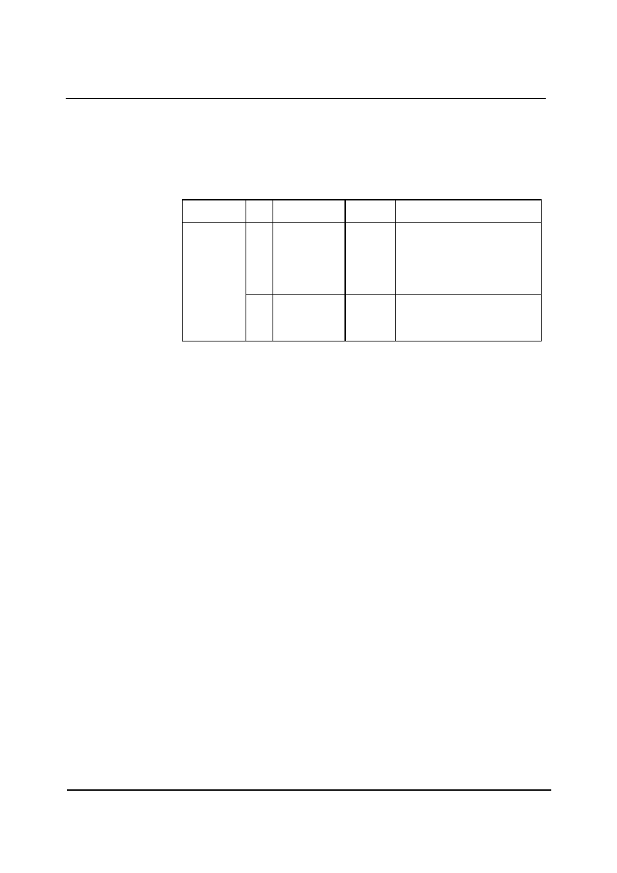
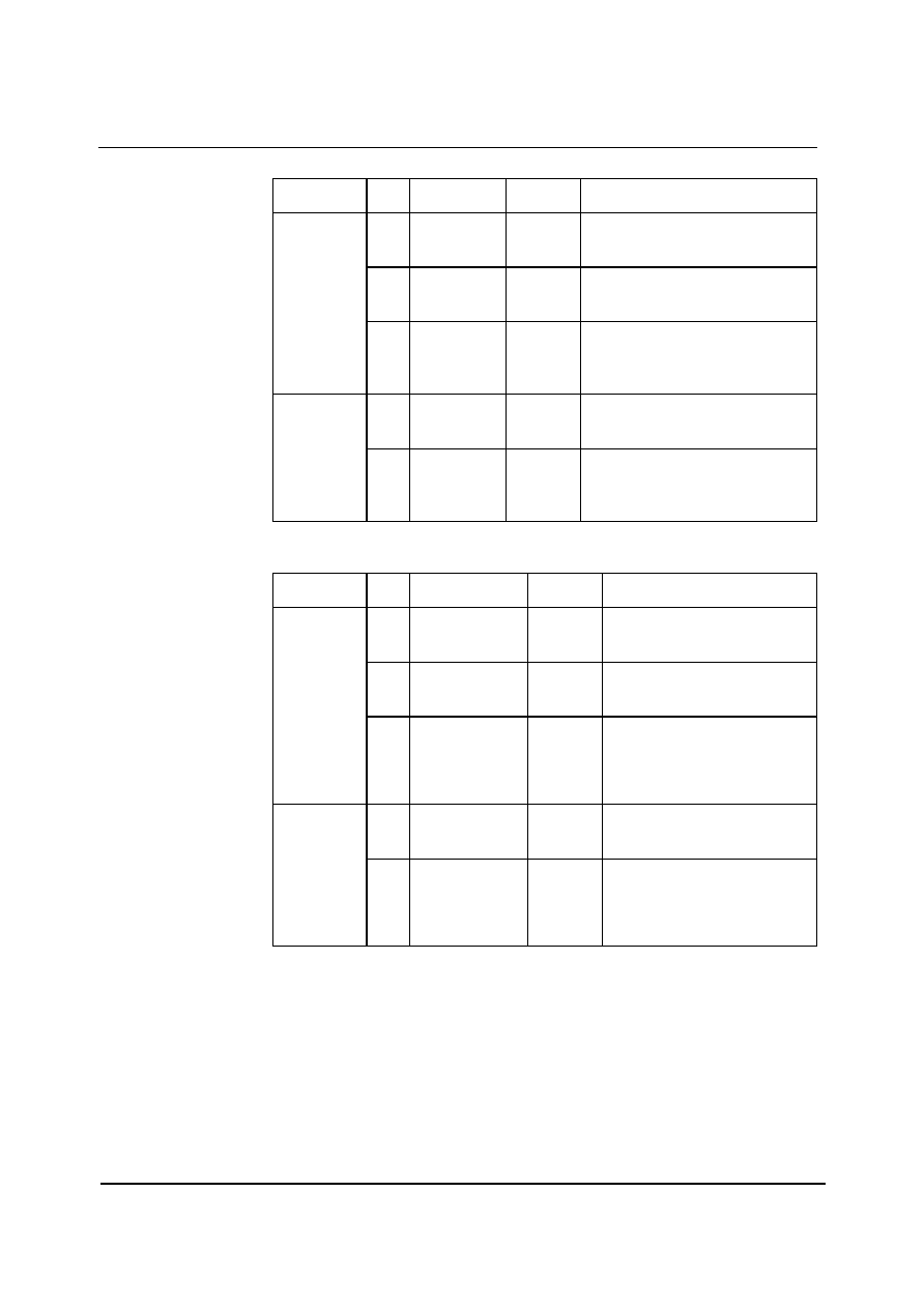
ELECTRICAL CHARACTERISTICS
Test Conditions
DCVDD = 1.5V, DBVDD = 3.3V, AVDD = OPVDD = 3.3V, T
A
= +25
o
C, 1kHz signal, fs = 48kHz, PGA gain = 0dB, 24-bit audio
data unless otherwise stated.
PARAMETER
SYMBOL
TEST CONDITIONS
MIN
TYP
MAX
UNIT
Analogue Inputs (LINPUT1, RINPUT1, LINPUT2, RINPUT2, LINPUT3, RINPUT3) to ADC out
AVDD = 3.3V
1.0
Full Scale Input Signal Level
(for ADC 0dB Input at 0dB Gain)
V
INFS
AVDD = 1.8V
0.545
V rms
+/-INPUT1 to ADC,
PGA gain = 0dB
22
+/-INPUT1 to ADC,
PGA gain = +30dB
1.5
DC Measurement
16
Input Resistance
+/-INPUT1 unused
17
k
Input Capacitance
10
pF
AVDD = 3.3V
80
95
Signal to Noise Ratio
(A-weighted)
SNR
AVDD = 1.8V
90
dB
Dynamic Range
-60dBFs
90
95
dB
-1dBFs input,
AVDD = 3.3V
-82
0.008
-77
0.014
Total Harmonic Distortion
THD
-1dBFs input,
AVDD = 1.8V
-74
0.02
dB
%
Analogue Outputs (OUT+/-, MONOOUT)
0dB Full scale output voltage
AVDD/3.3
Vrms
1kHz, full scale signal
90
Mute attenuation
MONOOUT pin
81
dB
DAC to Line-Out (OUT+/- with 10k
/ 50pF load)
AVDD=3.3V
90
98
Signal to Noise Ratio
(A-weighted)
SNR
AVDD=1.8V
93
dB
AVDD=3.3V
-84
Total Harmonic Distortion
THD
AVDD=1.8V
-80
dB
Speaker Output (OUT +/- with 8
bridge tied load, OUTINV=1)
Output Power
P
O
Output power is very closely correlated with THD; see below.
Po=180mW, R
L
=8
,
OPVDD=3.3V
-60
0.1
Total Harmonic Distortion
THD
Po=400mW, R
L
=8
OPVDD=3.3V
-36
1.6
dB
%
Signal to Noise Ratio
(A-weighted)
SNR
OPVDD=3.3V, R
L
=8
95
dB
Analogue Reference Levels
Midrail Reference Voltage
VMID
≠3%
AVDD/2
+3%
V
Buffered Reference Voltage
VREF
≠3%
AVDD/2
+3%
V
Microphone Bias
Bias Voltage
V
MICBIAS
3mA load current
≠5%
0.9
◊AVDD
+ 5%
V
Bias Current Source
I
MICBIAS
3
mA
Output Noise Voltage
Vn
1K to 20kHz
15
nV/
Hz
Digital Input / Output
Input HIGH Level
V
IH
0.7
◊DBVDD
V
Input LOW Level
V
IL
0.3
◊DBVDD
V
Output HIGH Level
V
OH
I
OL
=1mA
0.9
◊DBVDD
V
Output LOW Level
V
OL
I
OH
-1mA
0.1
◊DBVDD
V
Preliminary Technical Data
WM8972L
w
PTD Rev 2.2 June 2004
7
OUTPUT PGA'S LINEARITY
Output PGA Gains
-70.000
-60.000
-50.000
-40.000
-30.000
-20.000
-10.000
0.000
10.000
40
50
60
70
80
90
100
110
120
130
XXXVOL Register Setting (binary)
Meas
u
r
ed G
ain [d
B
]
OUT+
OUT-
MONOOUT
Output PGA Gain Step Size
0
0.25
0.5
0.75
1
1.25
1.5
1.75
2
40
50
60
70
80
90
100
110
120
130
XXXVOL Register Setting (binary)
S
t
e
p
S
iz
e [
d
B
]
OUT+
OUT-
MONOOUT
WM8972L
Preliminary Technical Data
w
PTD Rev 2.2 June 2004
8
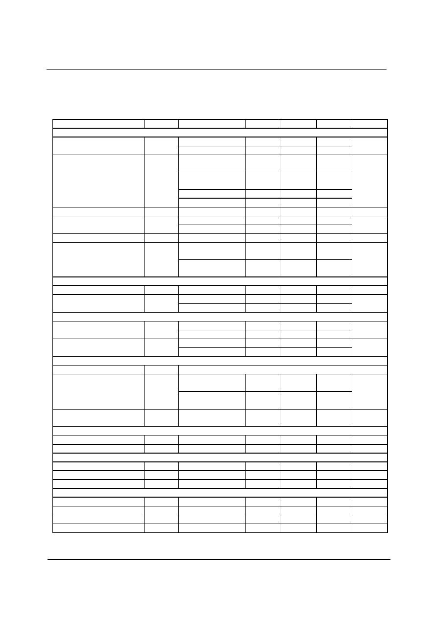
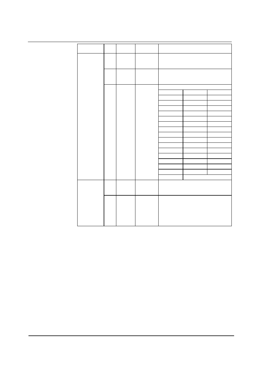
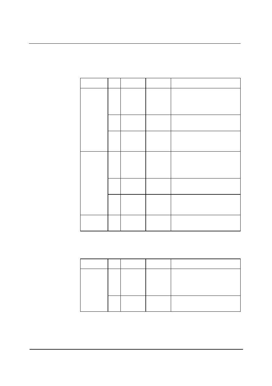
POWER CONSUMPTION
The power consumption of the WM8972L depends on the following factors.
∑
Supply voltages: Reducing the supply voltages also reduces supply currents, and therefore results in significant power
savings, especially in the digital sections of the WM8972L.
∑
Operating mode: Significant power savings can be achieved by always disabling parts of the WM8972L that are not
used (e.g. mic pre-amps, unused outputs, DAC, ADC, etc.)
Control Register
R23
Other settings
Tot. Power
Bit
VM
ID
SE
L
VR
EF
AI
N
AD
C
MI
C
B
DA
C
OU
T+
OU
T-
MO
N
O
OU
T2
AD
CO
S
R
DA
CO
S
R
VS
EL
V
I (mA)
V
I (mA)
V
I (mA)
V
I (mA)
mW
OFF
00 0 0 0 0 0 0 0 0 0 0 0 11
Clocks stopped
3.3 0.0016 3.3 0.0190 3.3 0.0080 3.3 0.0002
0.0950
01
2.5 0.0008 2.5 0.0170 2.5 0.0050 2.5 0.0000
0.0570
00
1.8 0.0005 1.5 0.0120 1.5 0.0029 1.8 0.0000
0.0233
Standby
10 1 0 0 0 0 0 0 0 0 0 0 11
Interface Stopped
3.3 0.3900 3.3 0.0390 3.3 0.0080 3.3 0.0000
1.4421
(500 KOhm VMID string)
01
2.5 0.2880 2.5 0.0170 2.5 0.0050 2.5 0.0000
0.7750
00
1.8 0.1970 1.5 0.0120 1.5 0.0030 1.8 0.0000
0.3771
Playback to 8 Ohm BTL Speaker 01 1 0 0 0 1 1 1 0 0 0 0 11
R24, OUTINV=1
3.3
TBD
3.3
TBD
3.3
TBD
3.3
TBD
TBD
01
2.5
TBD
2.5
TBD
2.5
TBD
2.5
TBD
TBD
00
1.8
TBD
1.5
TBD
1.5
TBD
1.8
TBD
TBD
Speaker Amp
01 1 0 0 0 0 1 1 0 0 0 0 11
Clocks Stopped
3.3 1.9780 3.3 0.0200 3.3 0.0080 3.3 0.3310
7.7121
(line-in to 8 Ohm speaker)
01
R24, OUTINV=1
2.5 1.4300 2.5 0.0190 2.5 0.0050 2.5 0.2430
4.2425
00
1.8 0.9860 1.5 0.0130 1.5 0.0030 1.8 0.1760
2.1156
Phone Call
01 1 0 0 1 0 1 1 1 0 0 0 11
Clocks Stopped
3.3 2.5230 3.3 0.0370 3.3 0.0080 3.3 0.4420
9.9330
(mono line-in to headphone,
01
2.5 1.8520 2.5 0.0190 2.5 0.0050 2.5 0.3200
5.4900
mic to MONOOUT)
00
1.8 1.2900 1.5 0.0130 1.5 0.0030 1.8 0.2240
2.7492
Record from Line-in
01 1 1 1 0 0 0 0 0 0 0 0 11
3.3
TBD
3.3
TBD
3.3
TBD
3.3
TBD
TBD
01
2.5
TBD
2.5
TBD
2.5
TBD
2.5
TBD
TBD
00
1.8
TBD
1.5
TBD
1.5
TBD
1.8
TBD
TBD
Record from Line-in
01 1 1 1 0 0 0 0 0 0 1 0 11
3.3
TBD
3.3
TBD
3.3
TBD
3.3
TBD
TBD
(64x oversampling mode)
01
2.5
TBD
2.5
TBD
2.5
TBD
2.5
TBD
TBD
00
1.8
TBD
1.5
TBD
1.5
TBD
1.8
TBD
TBD
Record from mono microphone
01 1 1 1 1 0 0 0 0 0 0 0 11 R32, MICBOOST=11; 3.3 4.9330 3.3 6.5400 3.3 0.3390 3.3 0.0000
38.9796
01
R23, DATSEL=01
2.5 4.2970 2.5 4.2500 2.5 0.2400 2.5 0.0000
21.9675
00
1.8 3.7210 1.5 2.2200 1.5 0.1370 1.8 0.0000
10.2333
Record from mono microphone
01 1 1 1 1 0 0 0 0 0 0 0 11 R32, MICBOOST=11; 3.3 5.2900 3.3 6.5000 3.3 0.3220 3.3 0.0000
39.9696
(differential)
01
R23, DATSEL=01;
2.5 4.5600 2.5 4.2700 2.5 0.2400 2.5 0.0000
22.6750
00
R32, INSEL=11
1.8 3.9000 1.5 2.2200 1.5 0.1380 1.8 0.0000
10.5570
Record & Playback
01 1 1 1 1 1 1 1 0 0 0 0 11
3.3
TBD
3.3
TBD
3.3
TBD
3.3
TBD
TBD
01
2.5
TBD
2.5
TBD
2.5
TBD
2.5
TBD
TBD
00
1.8
TBD
1.5
TBD
1.5
TBD
1.8
TBD
TBD
Record & Playback
01 1 1 1 1 1 1 1 0 0 1 1 11
3.3
TBD
3.3
TBD
3.3
TBD
3.3
TBD
TBD
(64x oversampling mode)
01
2.5
TBD
2.5
TBD
2.5
TBD
2.5
TBD
TBD
00
1.8
TBD
1.5
TBD
1.5
TBD
1.8
TBD
TBD
DBVDD
HPVDD
R24
R25 (19h)
R26 (1Ah)
AVDD
DCVDD
Table 1 Supply Current Consumption
Notes:
1.
All figures are at T
A
= +25
o
C, Slave Mode, fs = 48kHz, MCLK = 12.288 MHz (256fs), with zero signal (quiescent)
2.
The power dissipated in the headphone or speaker is not included in the above table.
Preliminary Technical Data
WM8972L
w
PTD Rev 2.2 June 2004
9
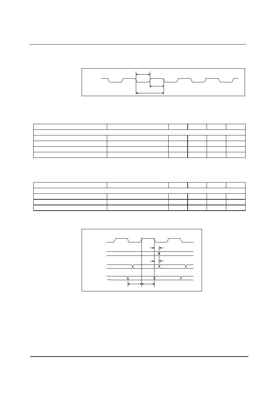
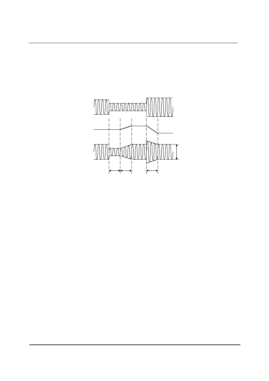
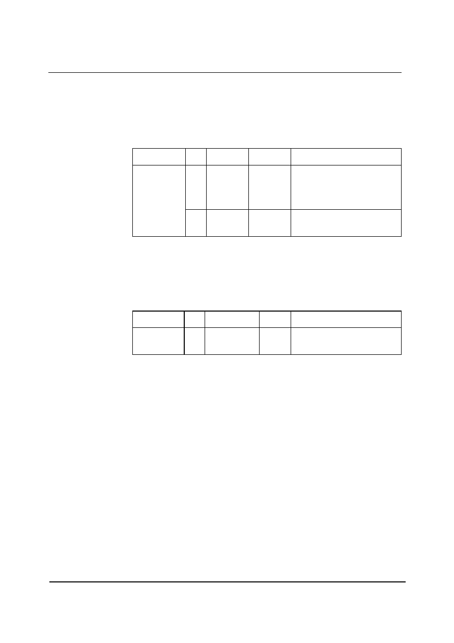
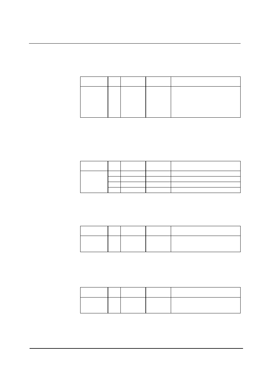
SIGNAL TIMING REQUIREMENTS
SYSTEM CLOCK TIMING
MCLK
t
MCLKL
t
MCLKH
t
MCLKY
Figure 1 System Clock Timing Requirements
Test Conditions
CLKDIV2=0, DCVDD = 1.42V, DBVDD = 3.3V, DGND = 0V, T
A
= +25
o
C, Slave Mode fs = 48kHz, MCLK = 384fs, 24-bit data,
unless otherwise stated.
PARAMETER
SYMBOL
MIN
TYP
MAX
UNIT
System Clock Timing Information
MCLK System clock pulse width high
T
MCLKL
21
ns
MCLK System clock pulse width low
T
MCLKH
21
ns
MCLK System clock cycle time
T
MCLKY
54
ns
MCLK duty cycle
T
MCLKDS
60:40
40:60
Test Conditions
CLKDIV2=1, DCVDD = 1.42V, DBVDD = 3.3V, DGND = 0V, T
A
= +25
o
C, Slave Mode fs = 48kHz, MCLK = 384fs, 24-bit data,
unless otherwise stated.
PARAMETER
SYMBOL
MIN
TYP
MAX
UNIT
System Clock Timing Information
MCLK System clock pulse width high
T
MCLKL
10
ns
MCLK System clock pulse width low
T
MCLKH
10
ns
MCLK System clock cycle time
T
MCLKY
27
ns
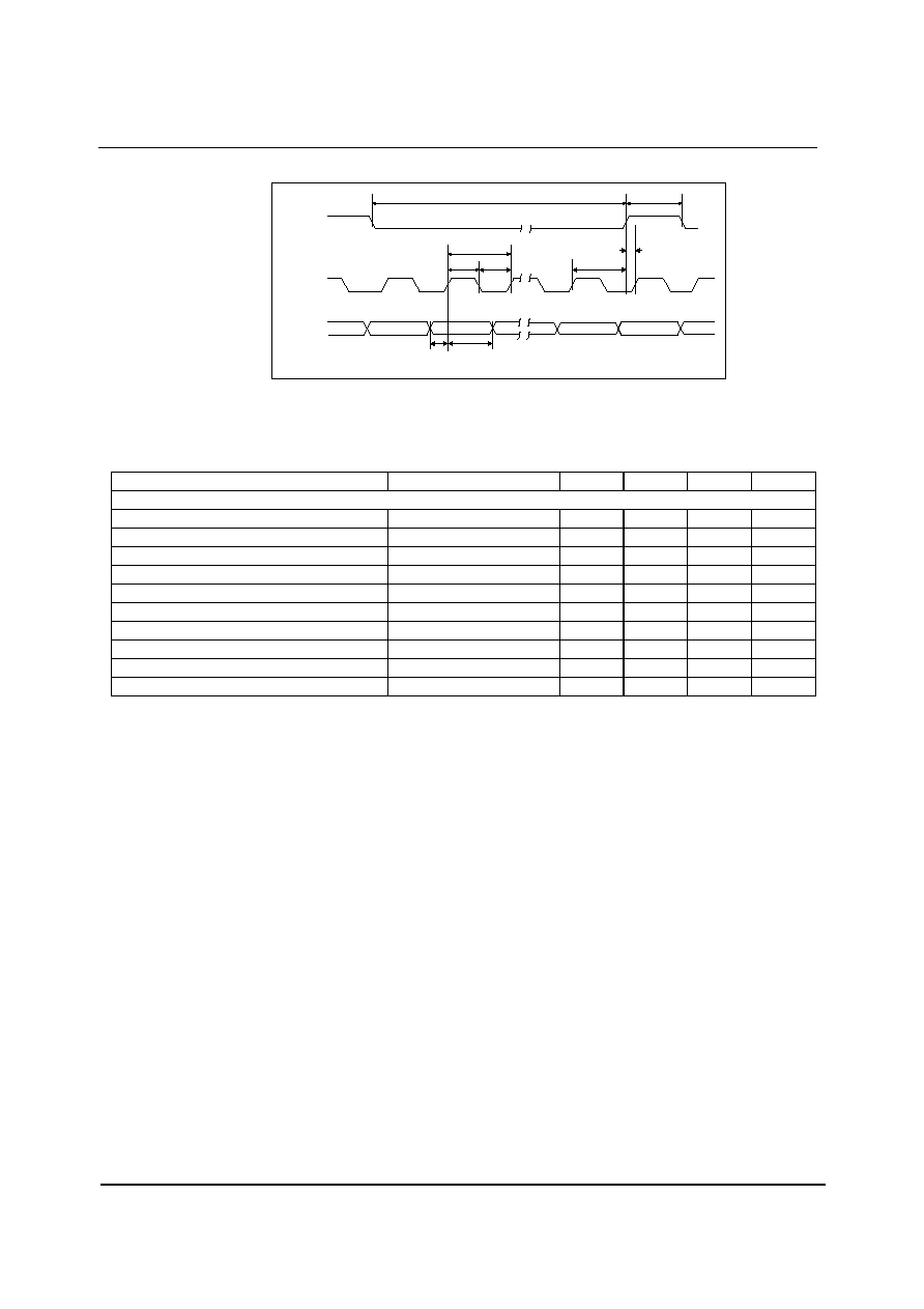
AUDIO INTERFACE TIMING ≠ MASTER MODE
BCLK
(Output)
ADCDAT
ADCLRC/
DACLRC
(Outputs)
t
DL
DACDAT
t
DDA
t
DHT
t
DST
Figure 2 Digital Audio Data Timing ≠ Master Mode (see Control Interface)
WM8972L
Preliminary Technical Data
w
PTD Rev 2.2 June 2004
10
Test Conditions
DCVDD = 1.42V, DBVDD = 3.3V, DGND = 0V, T
A
= +25
o
C, Slave Mode, fs = 48kHz, MCLK = 256fs, 24-bit data, unless
otherwise stated.
PARAMETER
SYMBOL
MIN
TYP
MAX
UNIT
Bit Clock Timing Information
BCLK rise time (10pF load)
t
BCLKR
3
ns
BCLK fall time (10pF load)
t
BCLKF
3
ns
BCLK duty cycle (normal mode, BCLK = MCLK/n)
t
BCLKDS
50:50
BCLK duty cycle (USB mode, BCLK = MCLK)
t
BCLKDS
T
MCLKDS
Audio Data Input Timing Information
ADCLRC/DACLRC propagation delay from BCLK falling edge
t
DL
10
ns
ADCDAT propagation delay from BCLK falling edge
t
DDA
10
ns
DACDAT setup time to BCLK rising edge
t
DST
10
ns
DACDAT hold time from BCLK rising edge
t
DHT
10
ns
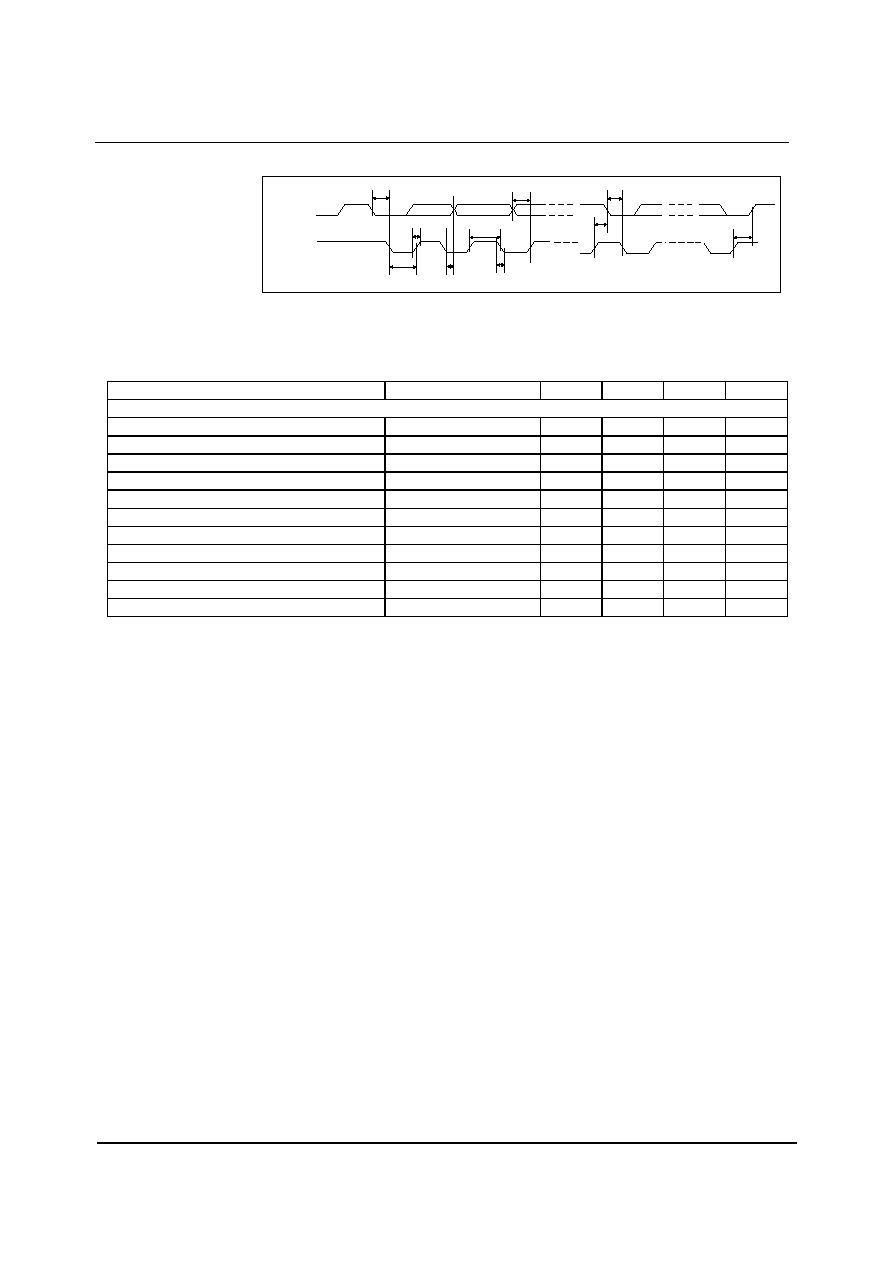
AUDIO INTERFACE TIMING ≠ SLAVE MODE
BCLK
DACLRC/
ADCLRC
t
BCH
t
BCL
t
BCY
DACDAT
ADCDAT
t
LRSU
t
DS
t
LRH
t
DH
t
DD
Figure 3 Digital Audio Data Timing ≠ Slave Mode
Test Conditions
DCVDD = 1.42V, DBVDD = 3.3V, DGND = 0V, T
A
= +25
o
C, Slave Mode, fs = 48kHz, MCLK = 256fs, 24-bit data, unless
otherwise stated.
PARAMETER
SYMBOL
MIN
TYP
MAX
UNIT
Audio Data Input Timing Information
BCLK cycle time
t
BCY
50
ns
BCLK pulse width high
t
BCH
20
ns
BCLK pulse width low
t
BCL
20
ns
ADCLRC/DACLRC set-up time to BCLK rising edge
t
LRSU
10
ns
ADCLRC/DACLRC hold time from BCLK rising edge
t
LRH
10
ns
DACDAT hold time from BCLK rising edge
t
DH
10
ns
ADCDAT propagation delay from BCLK falling edge
t
DD
10
ns
Note:
BCLK period should always be greater than or equal to MCLK period.
Preliminary Technical Data
WM8972L
w
PTD Rev 2.2 June 2004
11
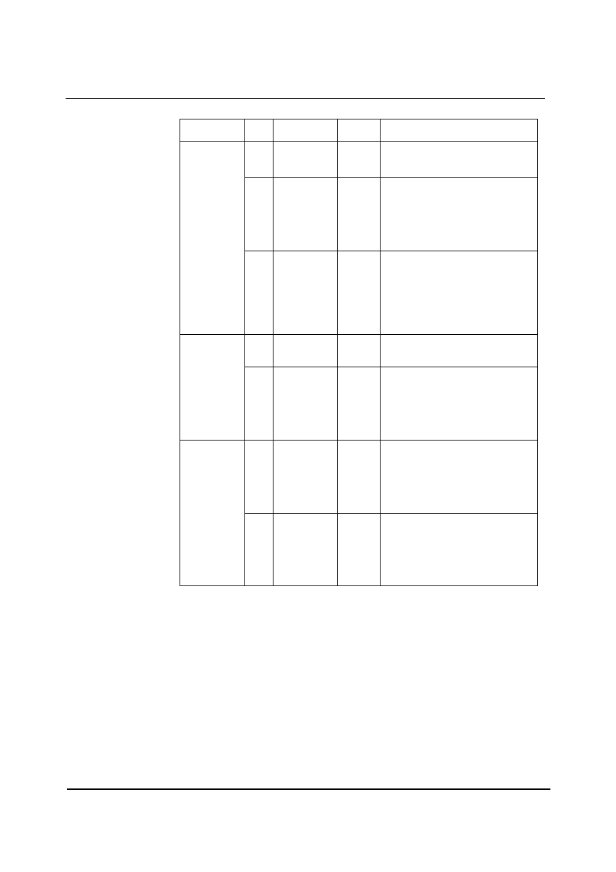
CONTROL INTERFACE TIMING ≠ 3-WIRE MODE
CSB
SCLK
SDIN
t
CSL
t
DHO
t
DSU
t
CSH
t
SCY
t
SCH
t
SCL
t
SCS
LSB
t
CSS
Figure 4 Control Interface Timing ≠ 3-Wire Serial Control Mode
Test Conditions
DCVDD = 1.42V, DBVDD = 3.3V, DGND = 0V, T
A
= +25
o
C, Slave Mode, fs = 48kHz, MCLK = 256fs, 24-bit data, unless
otherwise stated.
PARAMETER
SYMBOL
MIN
TYP
MAX
UNIT
Program Register Input Information
SCLK rising edge to CSB rising edge
t
SCS
80
ns
SCLK pulse cycle time
t
SCY
200
ns
SCLK pulse width low
t
SCL
80
ns
SCLK pulse width high
t
SCH
80
ns
SDIN to SCLK set-up time
t
DSU
40
ns
SCLK to SDIN hold time
t
DHO
40
ns
CSB pulse width low
t
CSL
40
ns
CSB pulse width high
t
CSH
40
ns
CSB rising to SCLK rising
t
CSS
40
ns
Pulse width of spikes that will be suppressed
t
ps
5
ns
WM8972L
Preliminary Technical Data
w
PTD Rev 2.2 June 2004
12
CONTROL INTERFACE TIMING ≠ 2-WIRE MODE
SDIN
SCLK
t
3
t
1
t
6
t
2
t
7
t
5
t
4
t
3
t
8
t
9
Figure 5 Control Interface Timing ≠ 2-Wire Serial Control Mode
Test Conditions
DCVDD = 1.42V, DBVDD = 3.3V, DGND = 0V, T
A
= +25
o
C, Slave Mode, fs = 48kHz, MCLK = 256fs, 24-bit data, unless
otherwise stated.
PARAMETER
SYMBOL
MIN
TYP
MAX
UNIT
Program Register Input Information
SCLK Frequency
0
400
kHz
SCLK Low Pulse-Width
t
1
600
ns
SCLK High Pulse-Width
t
2
1.3
us
Hold Time (Start Condition)
t
3
600
ns
Setup Time (Start Condition)
t
4
600
ns
Data Setup Time
t
5
100
ns
SDIN, SCLK Rise Time
t
6
300
ns
SDIN, SCLK Fall Time
t
7
300
ns
Setup Time (Stop Condition)
t
8
600
ns
Data Hold Time
t
9
900
ns
Pulse width of spikes that will be suppressed
t
ps
0
5
ns

Preliminary Technical Data
WM8972L
w
PTD Rev 2.2 June 2004
13
DEVICE DESCRIPTION
INTRODUCTION
The WM8972L is a low power audio CODEC offering a combination of high quality audio, advanced
features, low power and small size. These characteristics make it ideal for portable digital audio
applications such as digital still cameras and toys.
The device includes two differential analogue inputs that can be switched internally. Each can be
used as either a line level input or microphone input and INPUT1+/INPUT1- and INPUT2+/INPUT2-
can be configured as mono differential inputs. A programmable gain amplifier with automatic level
control (ALC) keeps the recording volume constant. The on-chip ADC and DAC are of a high quality
using a multi-bit, low-order oversampling architecture to deliver optimum performance with low power
consumption.
The DAC output signal first enters an analogue mixer where an analogue input and/or the post-ALC
signal can be added to it.
The WM8972L has a configurable digital audio interface where ADC data can be read and digital
audio playback data fed to the DAC. It supports a number of audio data formats including I
2
S, DSP
Mode (a burst mode in which frame sync plus 2 data packed words are transmitted), MSB-First, left
justified and MSB-First and right justified. It can operate in master or slave modes.
The WM8972L uses a unique clocking scheme that can generate many commonly used audio
sample rates from either a 12.00MHz USB clock or an industry standard 256/384 f
s
clock. This
feature eliminates the common requirement for an external phase-locked loop (PLL) in applications
where the master clock is not an integer multiple of the sample rate. Sample rates of 8kHz,
11.025kHz, 12kHz, 16kHz, 22.05kHz, 24kHz, 32kHz, 44.1kHz, 48kHz, 88.2kHz and 96kHz can be
generated. The digital filters used for recording and playback are optimised for each sampling rate
used.
To allow full software control over all its features, the WM8972L offers a choice of 2 or 3 wire MPU
control interface. It is fully compatible with and an ideal partner for a wide range of industry standard
microprocessors, controllers and DSPs.
The design of the WM8972L has given much attention to power consumption without compromising
performance. It operates at very low voltages, and includes the ability to power off parts of the
circuitry under software control, including standby and power off modes.
INPUT SIGNAL PATH
The input signal path for each channel consists of a switch to select between two analogue inputs,
followed by a PGA (programmable gain amplifier) and an optional microphone gain boost. A
differential input of either (INPUT1+ ≠ INPUT1-) or (INPUT2+ ≠ INPUT2-) may also be selected. The
gain of the PGA can be controlled either by the user or by the on-chip ALC function (see Automatic
Level Control). The signal then enters an ADC where it is digitised.
SIGNAL INPUTS
The WM8972L has two sets of high impedance, low capacitance AC coupled analogue inputs,
INPUT1+/INPUT1- and INPUT2+/INPUT2-. Inputs can be configured as microphone or line level by
enabling or disabling the microphone gain boost.
The INSEL control bits (see Table 2) are used to select independently between external inputs and
internally generated differential products. The choice of differential signal, INPUT1+ ≠ INPUT1- or
INPUT2+ ≠ INPUT2- is made using DS (refer to Table 3).
As an example, the WM8972 can be set up to convert one differential input and route a single ended
signal through the bypass path to the output mixing stage. This is done by applying the differential
signal to INPUT1+ and INPUT1- and the single ended signal to INPUT2-. By setting DS to INPUT1+
and INPUT1- (see Table 3) and +/-MIXSEL to INPUT2+/-, each mono signal can be routed
separately.
The inputs can also be configured as BEEP inputs by selecting the bypass path directly to the output
mixing stage. Two BEEP inputs are available if the bypass mode is not used for audio signals,
otherwise one BEEP input is available.
The signal inputs are biased internally to the reference voltage VREF. Whenever the line inputs are
muted or the device placed into standby mode, the inputs are kept biased to VREF using special
anti-thump circuitry. This reduces any audible clicks that may otherwise be heard when changing
inputs.
WM8972L
Preliminary Technical Data
w
PTD Rev 2.2 June 2004
14
REGISTER
ADDRESS
BIT
LABEL
DEFAULT
DESCRIPTION
7:6
INSEL
00
Input Select
00 = INPUT1
01 = INPUT2
11 = L-R Differential (either INPUT1+
≠ INPUT1- or INPUT2+ ≠
INPUT2-, selected by DS)
R32 (20h)
ADC Signal
Path Control
5:4
MICBOOST
00
Microphone Gain Boost
00 = Boost off (bypassed)
01 = 13dB boost
10 = 20dB boost
11 = 29dB boost
Table 2 Input Software Control
REGISTER
ADDRESS
BIT
LABEL
DEFAULT
DESCRIPTION
R31 (1Fh)
ADC Input Mode
8
DS
0
Differential input select
0: INPUT1+ ≠ INPUT1-
1: INPUT2+ ≠ INPUT2-
Table 3 Differential Input Select
The MICBIAS output provides a low noise reference voltage suitable for biasing electret type
microphones and the associated external resistor biasing network. Refer to the Applications
Information section for recommended external components. The output can be enabled or disabled
using the MICB control bit (see also the "Power Management" section).
REGISTER
ADDRESS
BIT
LABEL DEFAULT
DESCRIPTION
R25 (19h)
Power
Management (1)
1
MICB
0
Microphone Bias Enable
0 = OFF (high impedance output)
1 = ON
Table 4 Microphone Bias Control
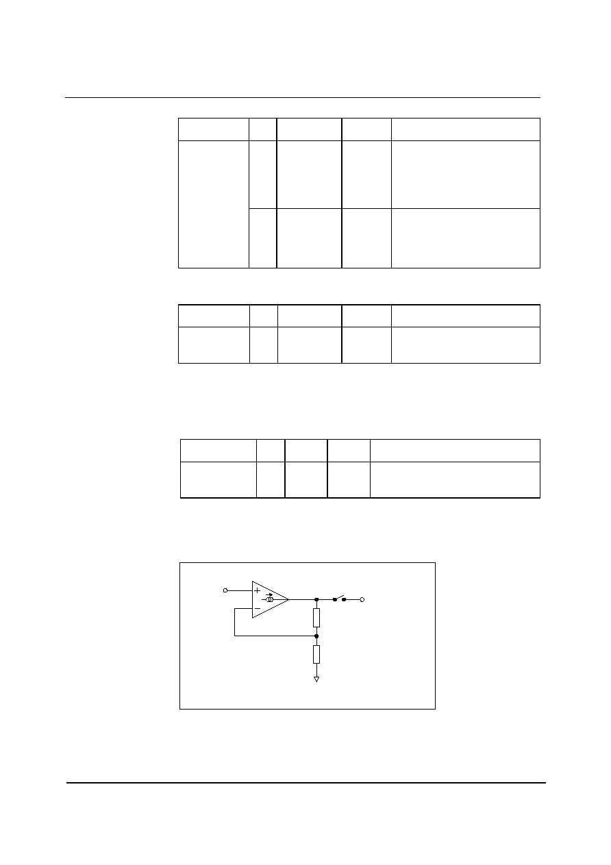
The internal MICBIAS circuitry is shown below. Note that the is a maximum source current capability
for MICBIAS is 3mA. The external biasing resistors therefore must be large enough to limit the
MICBIAS current to 3mA.
AGND
MICBIAS
= 1.8 x VMID
= 0.9 X AVDD
VMID
internal
resistor
internal
resistor
MICB
Figure 6 Microphone Bias Schematic
Preliminary Technical Data
WM8972L
w
PTD Rev 2.2 June 2004
15
PGA CONTROL
The PGA matches the input signal level to the ADC input range. The PGA gain is logarithmically
adjustable from +30dB to ≠17.25dB in 0.75dB steps. The PGA can be controlled either by the user or
by the ALC function (see Automatic Level Control). When ALC is enabled then writing to the PGA
control register has no effect.
Setting the ZCEN bit enables a zero-cross detector which ensures that PGA gain changes only occur
when the signal is at zero, eliminating any zipper noise. If zero cross is enabled a timeout is also
available to update the gain if a zero cross does not occur. This function may be enabled by setting
TOEN in register R23 (17h).
The inputs can also be muted in the analogue domain under software control. The software control
registers are shown in Table 5. If zero crossing is enabled, it is necessary to enable zero cross
timeout to un-mute the input PGAs. This is because their outputs will not cross zero when muted.
Alternatively, zero cross can be disables before sending the un-mute command.
REGISTER
ADDRESS
BIT
LABEL
DEFAULT
DESCRIPTION
8
IVU
0
Volume Update
0 = Store INVOL in intermediate
latch (no gain change)
1 = Update gains
7
INMUTE
1
Analogue Mute
1 = Enable Mute
0 = Disable Mute
Note: IVU must be set to un-mute.
6
ZCEN
0
Zero Cross Detector
1 = Change gain on zero cross only
0 = Change gain immediately
R0 (00h)
PGA
5:0
INVOL
[5:0]
010111
( 0dB )
Input Volume Control
111111 = +30dB
111110 = +29.25dB
. . 0.75dB steps down to
000000 = -17.25dB
R23 (17h)
Additional
Control (1)
0
TOEN
0
Timeout Enable
0 : Timeout Disabled
1 : Timeout Enabled
Table 5 Input PGA Software Control

WM8972L
Preliminary Technical Data
w
PTD Rev 2.2 June 2004
16
ANALOGUE TO DIGITAL CONVERTER (ADC)
The WM8972L uses a multi-bit, oversampled sigma-delta ADC. The use of multi-bit feedback and
high oversampling rates reduces the effects of jitter and high frequency noise. The ADC Full Scale
input level is proportional to AVDD. With a 3.3V supply voltage, the full scale level is 1.0 Volt r.m.s.
Any voltage greater than full scale may overload the ADC and cause distortion.
ADC DIGITAL FILTER
The ADC filters perform true 24 bit signal processing to convert the raw multi-bit oversampled data
from the ADC to the correct sampling frequency to be output on the digital audio interface. The digital
filter path is illustrated in Figure 7.
FROM ADC
DIGITAL
HPF
DIGITAL
FILTER
TO DIGITAL
AUDIO
INTERFACE
DIGITAL
DECIMATOR
ADCHPD
Figure 7 ADC Digital Filter
The ADC digital filters contain a digital high pass filter, selectable via software control. The high-pass
filter response is detailed in the Digital Filter Characteristics section. When the high-pass filter is
enabled the dc offset is continuously calculated and subtracted from the input signal. By setting
HPOR, the last calculated dc offset value is stored when the high-pass filter is disabled and will
continue to be subtracted from the input signal. If the DC offset is changed, the stored and
subtracted value will not change unless the high-pass filter is enabled. This feature can be used for
calibration purposes.
The output data format can be programmed by the user. The polarity of the output signal can also be
changed under software control. The software control is shown in Table 6.
REGISTER
ADDRESS
BIT
LABEL
DEFAULT
DESCRIPTION
5
ADCPOL
0
0 = Polarity not inverted
1 = Polarity invert
4
HPOR
0
Store dc offset when High Pass
Filter disabled
1 = store offset
0 = clear offset
R5 (05h)
ADC and DAC
Control
0
ADCHPD
0
ADC High Pass Filter Enable
(Digital)
1 = Disable High Pass Filter
0 = Enable High Pass Filter
Table 6 ADC Signal Path Control
Preliminary Technical Data
WM8972L
w
PTD Rev 2.2 June 2004
17
DIGITAL ADC VOLUME CONTROL
The output of the ADC can be digitally amplified or attenuated over a range from ≠97dB to +30dB in
0.5dB steps. The gain for a given eight-bit code X is given by:
0.5
◊ (X-195) dB for 1 X 255;
MUTE for X = 0
The AVU control bit controls the loading of digital volume control data. When AVU is set to 0, the
ADCVOL control data will be loaded into the control register, but will not actually change the digital
gain setting. Gain settings are updated when AVU is set to 1.
REGISTER
ADDRESS
BIT
LABEL
DEFAULT
DESCRIPTION
7:0
ADCVOL
[7:0]
11000011
( 0dB )
ADC Digital Volume Control
0000 0000 = Digital Mute
0000 0001 = -97dB
0000 0010 = -96.5dB
... 0.5dB steps up to
1111 1111 = +30dB
R21 (15h)
ADC Digital
Volume
8
AVU
0
ADC Volume Update
0 = Store ADCVOL in intermediate
latch (no gain change)
1 = Update gains ( = ADCVOL)
Table 7 ADC Digital Volume Control
WM8972L
Preliminary Technical Data
w
PTD Rev 2.2 June 2004
18
AUTOMATIC LEVEL CONTROL (ALC)
The WM8750L has an automatic level control that aims to keep a constant recording volume
irrespective of the input signal level. This is achieved by continuously adjusting the PGA gain so that
the signal level at the ADC input remains constant. A digital peak detector monitors the ADC output
and changes the PGA gain if necessary. Note that when the ALC function is enabled, the settings of
registers 0 and 1 (LINVOL, LIVU, LIZC, LINMUTE, RINVOL, RIVU, RIZC and RINMUTE) are
ignored.
hold
time
decay
time
attack
time
input
signal
signal
after
ALC
PGA
gain
ALC
target
level
Figure 8 ALC Operation
The ALC function is enabled using the ALCSEL control bits. When enabled, the recording volume
can be programmed between ≠6dB and ≠28.5dB (relative to ADC full scale) using the ALCL register
bits. An upper limit for the PGA gain can be imposed by setting the MAXGAIN control bits.
HLD, DCY and ATK control the hold, decay and attack times, respectively:
Hold time is the time delay between the peak level detected being below target and the PGA gain
beginning to ramp up. It can be programmed in power-of-two (2
n
) steps, e.g. 2.67ms, 5.33ms,
10.67ms etc. up to 43.7s. Alternatively, the hold time can also be set to zero. The hold time only
applies to gain ramp-up, there is no delay before ramping the gain down when the signal level is
above target.
Decay (Gain Ramp-Up) Time is the time that it takes for the PGA gain to ramp up across 90% of its
range (e.g. from ≠15B up to 27.75dB). The time it takes for the recording level to return to its target
value therefore depends on both the decay time and on the gain adjustment required. If the gain
adjustment is small, it will be shorter than the decay time. The decay time can be programmed in
power-of-two (2
n
) steps, from 24ms, 48ms, 96ms, etc. to 24.58s.
Attack (Gain Ramp-Down) Time is the time that it takes for the PGA gain to ramp down across 90%
of its range (e.g. from 27.75dB down to -15B gain). The time it takes for the recording level to return
to its target value therefore depends on both the attack time and on the gain adjustment required. If
the gain adjustment is small, it will be shorter than the attack time. The attack time can be
programmed in power-of-two (2
n
) steps, from 6ms, 12ms, 24ms, etc. to 6.14s.
Preliminary Technical Data
WM8972L
w
PTD Rev 2.2 June 2004
19
REGISTER
ADDRESS
BIT
LABEL
DEFAULT
DESCRIPTION
8
ALCSEL
0
(OFF)
ALC function select
0 = ALC off (PGA gain set by register)
1 = ALC on
6:4
MAXGAIN
[2:0]
111
(+30dB)
Set Maximum Gain of PGA
111 : +30dB
110 : +24dB
....(-6dB steps)
001 : -6dB
000 : -12dB
R17 (11h)
ALC Control 1
3:0
ALCL
[3:0]
1011
(-12dB)
ALC target ≠ sets signal level at ADC
input
0000 = -28.5dB FS
0001 = -27.0dB FS
... (1.5dB steps)
1110 = -7.5dB FS
1111 = -6dB FS
7
ALCZC
0 (zero
cross
off)
ALC uses zero cross detection circuit.
R18 (12h)
ALC Control 2
3:0
HLD
[3:0]
0000
(0ms)
ALC hold time before gain is increased.
0000 = 0ms
0001 = 2.67ms
0010 = 5.33ms
... (time doubles with every step)
1111 = 43.691s
7:4
DCY
[3:0]
0011
(192ms)
ALC decay (gain ramp-up) time
0000 = 24ms
0001 = 48ms
0010 = 96ms
... (time doubles with every step)
1010 or higher = 24.58s
R19 (13h)
ALC Control 3
3:0
ATK
[3:0]
0010
(24ms)
ALC attack (gain ramp-down) time
0000 = 6ms
0001 = 12ms
0010 = 24ms
... (time doubles with every step)
1010 or higher = 6.14s
Table 8 ALC Control
PEAK LIMITER
To prevent clipping when a large signal occurs just after a period of quiet, the ALC circuit includes a
limiter function. If the ADC input signal exceeds 87.5% of full scale (≠1.16dB), the PGA gain is
ramped down at the maximum attack rate (as when ATK = 0000), until the signal level falls below
87.5% of full scale. This function is automatically enabled whenever the ALC is enabled.
Note:
If ATK = 0000, then the limiter makes no difference to the operation of the ALC. It is designed to
prevent clipping when long attack times are used.
WM8972L
Preliminary Technical Data
w
PTD Rev 2.2 June 2004
20
NOISE GATE
When the signal is very quiet and consists mainly of noise, the ALC function may cause "noise
pumping", i.e. loud hissing noise during silence periods. The WM8972L has a noise gate function
that prevents noise pumping by comparing the signal level at the INPUT1+ and/or INPUT2+ pins
against a noise gate threshold, NGTH. The noise gate cuts in when:
∑
Signal level at ADC [dB] < NGTH [dB] + PGA gain [dB] + Mic Boost gain [dB]
This is equivalent to:
∑
Signal level at input pin [dB] < NGTH [dB]
The ADC output can then either be muted or the PGA gain can be held constant (preventing it from
ramping up as it normally would when the signal is quiet).
The table below summarises the noise gate control register. The NGTH control bits set the noise
gate threshold with respect to the ADC full-scale range. The threshold is adjusted in 1.5dB steps.
Levels at the extremes of the range may cause inappropriate operation, so care should be taken with
set≠up of the function. Note that the noise gate only works in conjunction with the ALC function.
REGISTER
ADDRESS
BIT
LABEL
DEFAULT
DESCRIPTION
7:3
NGTH
[4:0]
00000
Noise gate threshold
00000 -76.5dBfs
00001 -75dBfs
... 1.5 dB steps
11110 -31.5dBfs
11111 -30dBfs
2:1
NGG
[1:0]
00
Noise gate type
X0 = PGA gain held constant
01 = mute ADC output
11 = reserved (do not use this setting)
R20 (14h)
Noise Gate
Control
0
NGAT
0
Noise gate function enable
1 = enable
0 = disable
Table 9 Noise Gate Control
Note:
The performance of the ADC may degrade at high input signal levels if the monitor bypass mux is
selected with MIC boost and ALC enabled.
Preliminary Technical Data
WM8972L
w
PTD Rev 2.2 June 2004
21
OUTPUT SIGNAL PATH
The WM8972L output signal paths consist of digital filters, a DAC, analogue mixers and output
drivers. The digital filters and DAC are enabled when the WM8972L is in `playback only' or `record
and playback' mode. The mixers and output drivers can be separately enabled by individual control
bits (see Analogue Outputs). Thus it is possible to utilise the analogue mixing and amplification
provided by the WM8972L, irrespective of whether the DAC is running or not.
The WM8972L receives digital input data on the DACDAT pin. The digital filter block processes the
data to provide the following functions:
∑
Digital volume control
∑
Graphic equaliser and Dynamic Bass Boost
∑
Sigma-Delta Modulation
A high performance sigma-delta audio DAC converts the digital data into two analogue signals (left
and right). These can then be mixed with analogue signals from the INPUT1+/2+ and INPUT1-/2-
pins, and the mix is fed to the output drivers, OUT+/OUT-, OUT2 and MONOOUT.
∑
OUT2: can drive a 16
or 32 headphone or line output.
∑
OUT+/OUT-: can drive a 16
or 32 headphone or line output, or an 8 mono speaker.
∑
MONOOUT: can drive a mono line output or other load down to 10k
DIGITAL DAC VOLUME CONTROL
The signal volume from the DAC can be controlled digitally, in the same way as the ADC volume
(see Digital ADC Volume Control). The gain and attenuation range is ≠127dB to 0dB in 0.5dB steps.
The level of attenuation for an eight-bit code X is given by:
0.5
◊ (X-255) dB for 1 X 255;
MUTE for X = 0
The DVU control bit controls the loading of digital volume control data. When DVU is set to 0, the
DACVOL control data is loaded into an intermediate register, but the actual gain does not change.
The gain settings are updated simultaneously when DVU is set to 1.
REGISTER
ADDRESS
BIT
LABEL
DEFAULT
DESCRIPTION
8
DVU
0
DAC Volume Update
0 = Store DACVOL in intermediate
latch (no gain change)
1 = Update gains
R10 (0Ah)
Digital Volume
7:0
DACVOL
[7:0]
11111111
( 0dB )
DAC Digital Volume Control
0000 0000 = Digital Mute
0000 0001 = -127dB
0000 0010 = -126.5dB
... 0.5dB steps up to
1111 1111 = 0dB
Table 10 Digital Volume Control
GRAPHIC EQUALISER
The WM8972L has a digital graphic equaliser and adaptive bass boost function. This function
operates on digital audio data before it is passed to the audio DAC. Bass enhancement can take two
different forms:
∑
Linear bass control: bass signals are amplified or attenuated by a user programmable
gain. This is independent of signal volume, and very high bass gains on loud signals
may lead to signal clipping.
∑
Adaptive bass boost: The bass volume is amplified by a variable gain. When the bass
volume is low, it is boosted more than when the bass volume is high. This method is
recommended because it prevents clipping, and usually sounds more pleasant to the
human ear.
Treble control applies a user programmable gain, without any adaptive boost function. Bass and
treble control are completely independent with separately programmable gains and filter
characteristics.
WM8972L
Preliminary Technical Data
w
PTD Rev 2.2 June 2004
22
REGISTER
ADDRESS
BIT
LABEL
DEFAULT
DESCRIPTION
7
BB
0
Bass Boost
0 = Linear bass control
1 = Adaptive bass boost
6
BC
0
Bass Filter Characteristic
0 = Low Cutoff (130Hz at 48kHz sampling)
1 = High Cutoff (200Hz at 48kHz sampling)
Bass Intensity
Code
BB=0
BB=1
0000
+9dB
15 (max)
0001
+9dB
14
0010
+7.5dB
13
0011
+6dB
12
0100
+4.5dB
11
0101
+3dB
10
0110
+1.5dB
9
0111
0dB
8
1000
-1.5dB
7
1001
-3dB
6
1010
-4.5dB
5
1011
-6dB
4
1100
-6dB
3
1101
-6dB
2
1110
-6dB
1
R12 (0Ch)
Bass Control
3:0
BASS
[3:0]
1111
(Disabled)
1111
Bypass (OFF)
6
TC
0
Treble Filter Characteristic
0 = High Cutoff (8kHz at 48kHz sampling)
1 = Low Cutoff (4kHz at 48kHz sampling)
R13 (0Dh)
Treble Control
3:0
TRBL
[3:0]
1111
(Disabled)
Treble Intensity
0000 or 0001 = +9dB
0010 = +7.5dB
... (1.5dB steps)
1011 to 1110 = -6dB
1111 = Disable
Table 11 Graphic Equaliser
Preliminary Technical Data
WM8972L
w
PTD Rev 2.2 June 2004
23
DIGITAL TO ANALOGUE CONVERTER (DAC)
After passing through the graphic equaliser filters, digital `de-emphasis' can be applied to the audio
data if necessary (e.g. when the data comes from a CD with pre-emphasis used in the recording).
De-emphasis filtering is available for sample rates of 48kHz, 44.1kHz and 32kHz.
The WM8972L also has a Soft Mute function, which gradually attenuates the volume of the digital
signal to zero. When removed, the gain will ramp back up to the digital gain setting. This function is
enabled by default. To play back an audio signal, it must first be disabled by setting the DACMU bit
to zero.
REGISTER
ADDRESS
BIT
LABEL
DEFAULT
DESCRIPTION
2:1
DEEMP
[1:0]
00
De-emphasis Control
11 = 48kHz sample rate
10 = 44.1kHz sample rate
01 = 32kHz sample rate
00 = No De-emphasis
R5 (05h)
ADC and DAC
Control
3
DACMU
1
Digital Soft Mute
1 = mute
0 = no mute (signal active)
Table 12 DAC Control
The digital audio data is converted to oversampled bit streams in the on-chip, true 24-bit digital
interpolation filters. The bitstream data enters two multi-bit, sigma-delta DACs, which convert them to
high quality analogue audio signals. The multi-bit DAC architecture reduces high frequency noise and
sensitivity to clock jitter. It also uses a Dynamic Element Matching technique for high linearity and
low distortion.
The DAC output defaults to non-inverted. Setting DACINV will invert the DAC output phase on both
left and right channels.
REGISTER
ADDRESS
BIT
LABEL
DEFAULT
DESCRIPTION
R23 (17h)
Additional
Control (1)
1
DACINV
0
DAC phase invert
0 : non-inverted
1 : inverted
Table 13 Phase Invert Select
WM8972L
Preliminary Technical Data
w
PTD Rev 2.2 June 2004
24
OUTPUT MIXERS
The WM8972L provides the option to mix the DAC output signal with analogue line-in signals from
the INPUT1+/- or INPUT2+/- pins or a mono differential input (INPUT1+ ≠ INPUT1-) or (INPUT2+ ≠
INPUT2-), selected by DS (see Table 3). The level of the mixed-in signals can be controlled with
PGA (Programmable Gain Amplifier).
REGISTER
ADDRESS
BIT
LABEL
DEFAULT
DESCRIPTION
R34 (22h)
Plus Mixer (1)
2:0
+MIXSEL
000
Plus Input Selection for Output Mix
000 = INPUT1+
001 = INPUT2+
011 = ADC Input (after PGA /
MICBOOST)
100 = Differential input
R36 (24h)
Minus Mixer
(1)
2:0
-MIXSEL
000
Minus Input Selection for Output Mix
000 = INPUT1-
001 = INPUT2-
011 = RESERVED (Do not use)
100 = Differential input
Table 14 Output Mixer Signal Selection
REGISTER
ADDRESS
BIT
LABEL
DEFAULT
DESCRIPTION
8
D2+MO
0
DAC to Plus Mixer
0 = Disable (Mute)
1 = Enable Path
7
+M2+MO
0
+MIXSEL Signal to Plus Mixer
0 = Disable (Mute)
1 = Enable Path
R34 (22h)
Plus Mixer
Control (1)
6:4
+M2+MOVOL
[2:0]
101
(-9dB)
+MIXSEL Signal to Plus Mixer Volume
000 = +6dB
... (3dB steps)
111 = -15dB
7
-M2+MO
0
-MIXSEL Signal to Plus Mixer
0 = Disable (Mute)
1 = Enable Path
R35 (23h)
Plus Mixer
Control (2)
6:4
-M2+MOVOL
[2:0]
101
(-9dB)
-MIXSEL Signal to Plus Mixer Volume
000 = +6dB
... (3dB steps)
111 = -15dB
Table 15 Plus Output Mixer Control
Preliminary Technical Data
WM8972L
w
PTD Rev 2.2 June 2004
25
REGISTER
ADDRESS
BIT
LABEL
DEFAULT
DESCRIPTION
8
D2-MO
0
DAC to Minus Mixer
0 = Disable (Mute)
1 = Enable Path
7
+M2-MO
0
+MIXSEL Signal to Minus Mixer
0 = Disable (Mute)
1 = Enable Path
R36 (24h)
Minus Mixer
Control (1)
6:4
+M2-MOVOL
[2:0]
101
(-9dB)
+MIXSEL Signal to Minus Mixer Volume
000 = +6dB
... (3dB steps)
111 = -15dB
7
-M2-MO
0
-MIXSEL Signal to Minus Mixer
0 = Disable (Mute)
1 = Enable Path
R37 (25h)
Minus Mixer
Control (2)
6:4
-M2-MOVOL
[2:0]
101
(-9dB)
-MIXSEL Signal to Minus Mixer Volume
000 = +6dB
... (3dB steps)
111 = -15dB
Table 16 Minus Output Mixer Control
REGISTER
ADDRESS
BIT
LABEL
DEFAULT
DESCRIPTION
8
D2MO
0
DAC to Mono Mixer
0 = Disable (Mute)
1 = Enable Path
7
+M2MO
0
+MIXSEL Signal to Mono Mixer
0 = Disable (Mute)
1 = Enable Path
R38 (26h)
Mono Mixer
Control (1)
6:4
+M2MOVOL
[2:0]
101
(-9dB)
+MIXSEL Signal to Mono Mixer
Volume
000 = +6dB
... (3dB steps)
111 = -15dB
7
-M2MO
0
-MIXSEL Signal to Mono Mixer
0 = Disable (Mute)
1 = Enable Path
R39 (27h)
Mono Mixer
Control (2)
6:4
-M2MOVOL
[2:0]
101
(-9dB)
-MIXSEL Signal to Mono Mixer
Volume
000 = +6dB
... (3dB steps)
111 = -15dB
Table 17 Mono Output Mixer Control
WM8972L
Preliminary Technical Data
w
PTD Rev 2.2 June 2004
26
ANALOGUE OUTPUTS
OUT+/OUT- OUTPUTS
The OUT+ and OUT- output pins are independently controlled and can drive an 8
mono speaker
(see Speaker Output section). For speaker drive, the OUT- signal must be inverted (OUTINV = 1), so
that the two signals are mixed to mono in the speaker [OUT+ ≠ (-OUT-) = OUT+ + OUT-].
REGISTER
ADDRESS
BIT
LABEL
DEFAULT
DESCRIPTION
6:0
+OUTVOL
[6:0]
1111001
(0dB)
OUT+ Volume
1111111 = +6dB
... (80 steps)
0110000 = -67dB
0101111 to 0000000 = Analogue MUTE
7
+OZC
0
OUT+ zero cross enable
1 = Change gain on zero cross only
0 = Change gain immediately
R40 (28h)
OUT+
Volume
8
+OVU
0
OUT+ Volume Update
0 = Store +OUTVOL in intermediate
latch (no gain change)
1 = Update gains
6:0
-OUTVOL
[6:0]
1111001
(0dB)
OUT- Volume
1111111 = +6dB
... (80 steps)
0110000 = -67dB
0101111 to 0000000 = Analogue MUTE
7
-OZC
0
OUT- zero cross enable
1 = Change gain on zero cross only
0 = Change gain immediately
R41 (29h)
OUT-
Volume
8
-OVU
0
OUT- Volume Update
0 = Store -OUTVOL in intermediate latch
(no gain change)
1 = Update gains
R24 (18h)
Additional
Control (2)
4
OUTINV
0
OUT- Invert
0 = No Inversion (0
∞ phase shift)
1 = Signal inverted (180
∞ phase shift)
Table 18 OUT+/OUT- Volume Control
MONO OUTPUT
The MONOOUT pin can drive a mono line output. The signal volume on MONOOUT can be adjusted
under software control by writing to MONOOUTVOL.
REGISTER
ADDRESS
BIT
LABEL
DEFAULT
DESCRIPTION
6:0
MONOOUT
VOL [6:0]
1111001
(0dB)
MONOOUT Volume
1111111 = +6dB
... (80 steps)
0110000 = -67dB
0101111 to 0000000 = Analogue MUTE
R42 (2Ah)
MONOOUT
Volume
7
MOZC
0
MONOOUT zero cross enable
1 = Change gain on zero cross only
0 = Change gain immediately
Table 19 MONOOUT Volume Control
Preliminary Technical Data
WM8972L
w
PTD Rev 2.2 June 2004
27
OUT2 OUTPUT
The OUT2 pin can drive a 16
or 32 headphone or a line output or be used as a DC reference for a
headphone output (see Headphone Output section). It can be selected to either drive out an inverted
OUT- or inverted MONOOUT for e.g. a differential output between OUT2 and MONOOUT.
OUT2SW selects the mode of operation required.
REGISTER
ADDRESS
BIT
LABEL
DEFAULT
DESCRIPTION
R24 (18h)
Additional
Control (2)
8:7
OUT2SW
[1:0]
00
OUT2 select
00 : VREF
01 : RESERVED (Do not use)
10 : MONOOUT
11 : minus mixer output (no volume
control through -OUTVOL)
Table 20 OUT2 Select
ENABLING THE OUTPUTS
Each analogue output of the WM8972L can be separately enabled or disabled. The analogue mixer
associated with each output is powered on or off along with the output pin. All outputs are disabled by
default. To save power, unused outputs should remain disabled.
Outputs can be enabled at any time, except when VREF is disabled (VR=0), as this may cause pop
noise (see "Power Management" and "Applications Information" sections)
REGISTER
ADDRESS
BIT
LABEL
DEFAULT
DESCRIPTION
4
OUT+
0
OUT+ Enable
3
OUT-
0
OUT- Enable
2
MONO
0
MONOOUT Enable
R26 (1Ah)
Power
Management
(2)
1
OUT2
0
OUT2 Enable
Table 21 Analogue Output Control
Whenever an analogue output is disabled, it remains connected to VREF (pin 20) through a resistor.
This helps to prevent pop noise when the output is re-enabled. The resistance between VREF and
each output can be controlled using the VROI bit in register 27. The default is low (1.5k
), so that
any capacitors on the outputs can charge up quickly at start-up. If a high impedance is desired for
disabled outputs, VROI can then be set to 1, increasing the resistance to about 40k
.
REGISTER
ADDRESS
BIT
LABEL
DEFAULT
DESCRIPTION
R27 (1Bh)
Additional (1)
6
VROI
0
VREF to analogue output resistance
0: 1.5 k
1: 40 k
Table 22 Disabled Outputs to VREF Resistance
THERMAL SHUTDOWN
The speaker output can drive very large currents. To protect the WM8972L from overheating a
thermal shutdown circuit is included. If the device temperature reaches approximately 150
0
C and the
thermal shutdown circuit is enabled (TSDEN = 1 ) then the speaker outputs will be disabled.
REGISTER
ADDRESS
BIT
LABEL
DEFAULT
DESCRIPTION
R23 (17h)
Additional
Control (1)
8
TSDEN
0
Thermal Shutdown Enable
0 : thermal shutdown disabled
1 : thermal shutdown enabled
Table 23 Thermal Shutdown
WM8972L
Preliminary Technical Data
w
PTD Rev 2.2 June 2004
28
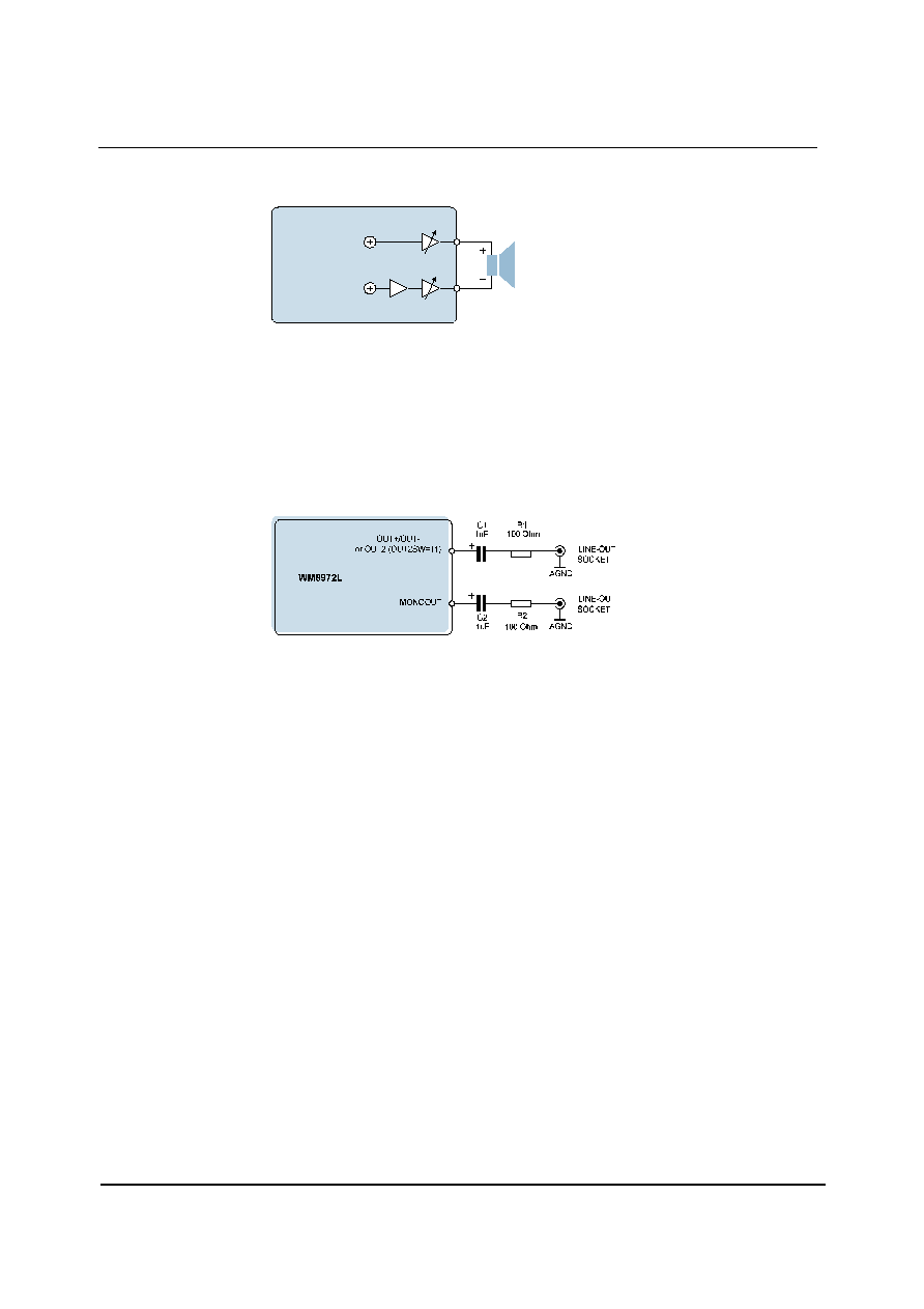
SPEAKER OUTPUT
OUT+ and OUT- can differentially drive a mono 8
speaker as shown below.
Figure 9 Speaker Output Connection
The OUT- channel is inverted by setting the OUTINV bit, so that the signal across the loudspeaker is
the sum of OUT+ and OUT- signals.
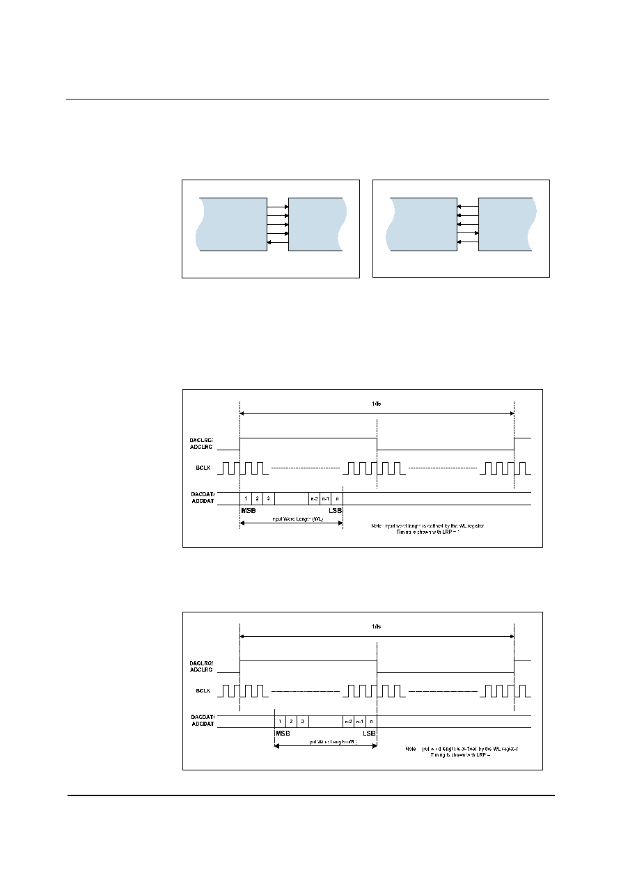
LINE OUTPUT
The analogue outputs OUT+/OUT- can be used as line outputs. Recommended external components
are shown below.
Figure 10 Recommended Circuit for Line Output
The DC blocking capacitors and the load resistance together determine the lower cut-off frequency,
f
c
. Assuming a 10 kOhm load and C1, C2 = 1
µF:
f
c
= 1 / 2
(R
L
+R
1
) C
1
= 1 / (2
x 10.1k x 1µF) = 16 Hz
Increasing the capacitance lowers f
c
, improving the bass response. Smaller values of C1 and C2 will
diminish the bass response. The function of R1 and R2 is to protect the line outputs from damage
when used improperly.
DIGITAL AUDIO INTERFACE
The digital audio interface is used for inputting DAC data into the WM8972L and outputting ADC data
from it. It uses five pins:
∑
ADCDAT: ADC data output
∑
ADCLRC: ADC data alignment clock
∑
DACDAT: DAC data input
∑
ADCLRC: DAC data alignment clock
∑
BCLK: Bit clock, for synchronisation
The clock signals BCLK, ADCLRC and DACLRC can be outputs when the WM8972L operates as a
master, or inputs when it is a slave (see Master and Slave Mode Operation, below).
Four different audio data formats are supported:
∑
Left justified
∑
Right justified
∑
I
2
S
∑
DSP mode
All four of these modes are MSB first. They are described in Audio Data Formats, below. Refer to the
Electrical Characteristic section for timing information.
OUT+
OUT-
WM8972L
ROUT2INV = 1
V
SPKR
= OUT+ -(-OUT-) = (OUT+) + (OUT-)
-1
PLUS MIXER
MINUS MIXER
-OUTVOL
+OUTVOL
Preliminary Technical Data
WM8972L
w
PTD Rev 2.2 June 2004
29
MASTER AND SLAVE MODE OPERATION
The WM8972L can be configured as either a master or slave mode device. As a master device the
WM8972L generates BCLK, ADCLRC and DACLRC and thus controls sequencing of the data
transfer on ADCDAT and DACDAT. In slave mode, the WM8972L responds with data to clocks it
receives over the digital audio interface. The mode can be selected by writing to the MS bit (see
Table 23). Master and slave modes are illustrated below.
Figure 11 Master Mode
Figure 12 Slave Mode
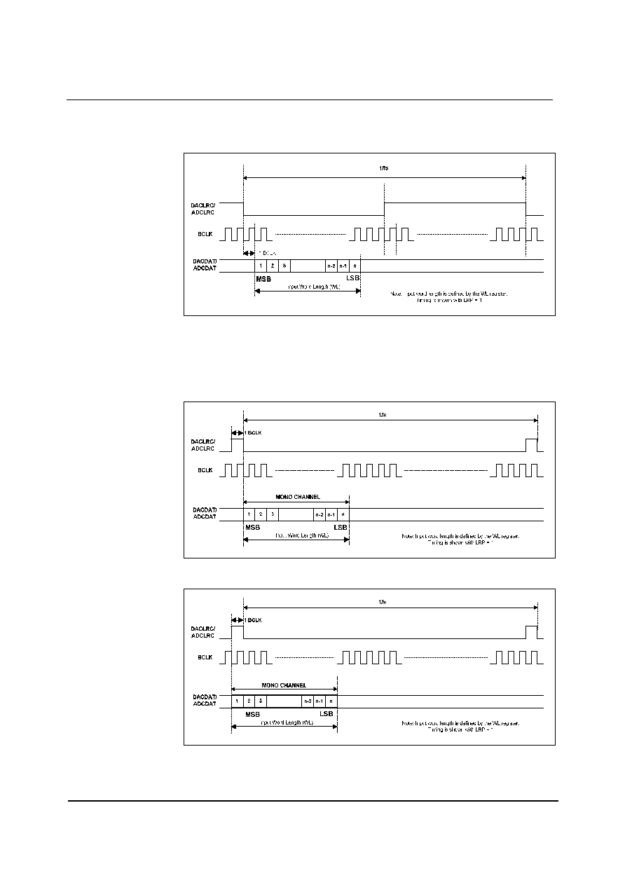
AUDIO DATA FORMATS
The mono data is available during the left channel period of DACLRC/ADCLRC.
In Left Justified mode, the MSB is available on the first rising edge of BCLK following a LRCLK
transition. The other bits up to the LSB are then transmitted in order. Depending on word length,
BCLK frequency and sample rate, there may be unused BCLK cycles before each LRCLK transition.
Figure 13 Left Justified Audio Interface (assuming n-bit word length)
In Right Justified mode, the LSB is available on the last rising edge of BCLK before a LRCLK
transition. All other bits are transmitted before (MSB first). Depending on word length, BCLK
frequency and sample rate, there may be unused BCLK cycles after each LRCLK transition.
Figure 14 Right Justified Audio Interface (assuming n-bit word length)
BCLK
ADCDAT
ADCLRC
DACDAT
DACLRC
WM8972
CODEC
DSP
ENCODER/
DECODER
Note: The ADC and DAC can run at different sample rates
BCLK
ADCDAT
ADCLRC
DACDAT
DACLRC
WM8972
CODEC
DSP
ENCODER/
DECODER
Note: The ADC and DAC can run at different sample rates
WM8972L
Preliminary Technical Data
w
PTD Rev 2.2 June 2004
30
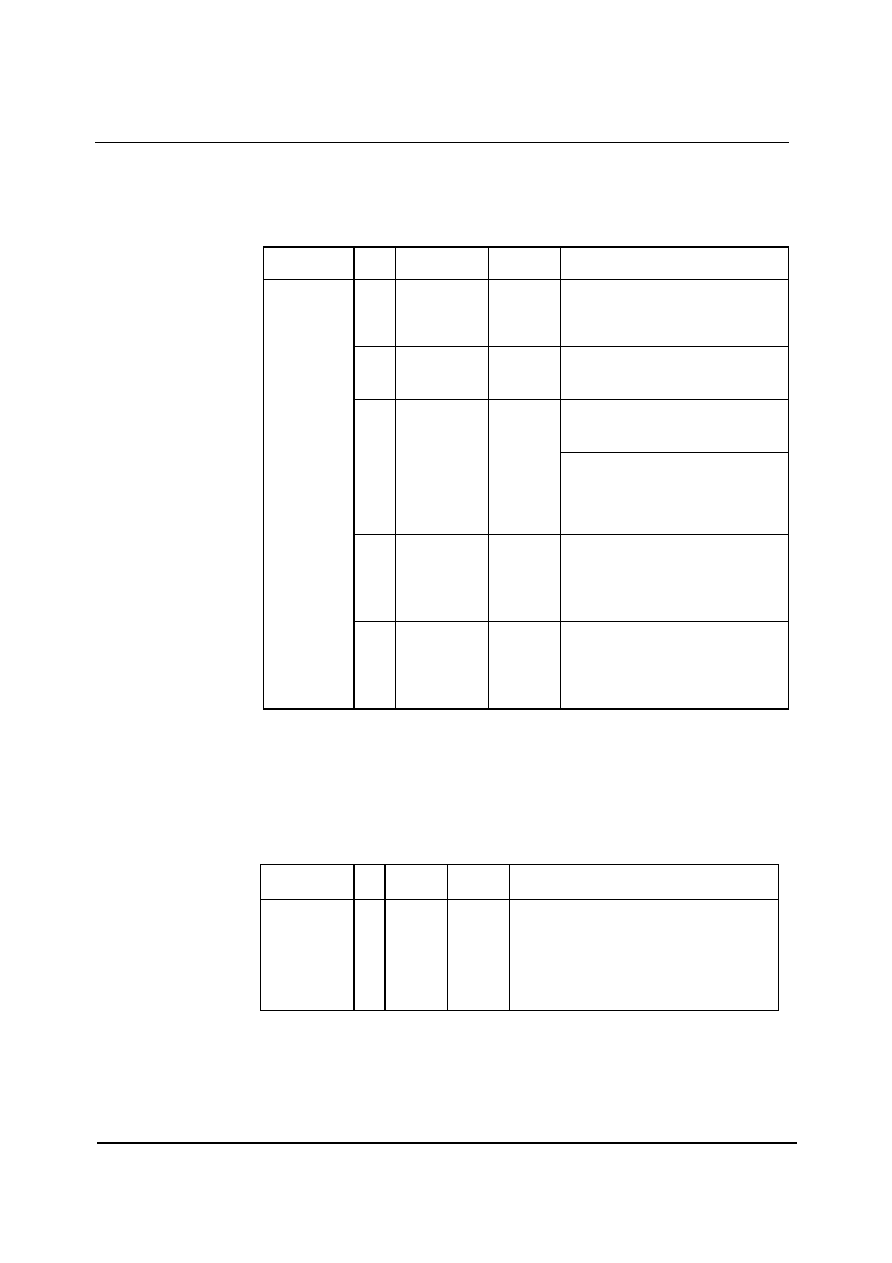
In I
2
S mode, the MSB is available on the second rising edge of BCLK following a LRCLK transition.
The other bits up to the LSB are then transmitted in order. Depending on word length, BCLK
frequency and sample rate, there may be unused BCLK cycles between the LSB of one sample and
the MSB of the next.
Figure 15 I
2
S Justified Audio Interface (assuming n-bit word length)
In DSP mode, the mono MSB is available on either the 1
st
(mode B) or 2
nd
(mode A) rising edge of
BCLK (selectable by LRP) following a rising edge of LRCLK. Depending on word length, BCLK
frequency and sample rate, there may be unused BCLK cycles between the LSB and the next
sample.
Figure 16 DSP Mode Audio Interface (mode A, LRP=0)
Figure 17 DSP Mode Audio Interface (mode B, LRP=1)
Preliminary Technical Data
WM8972L
w
PTD Rev 2.2 June 2004
31
AUDIO INTERFACE CONTROL
The register bits controlling audio format, word length and master / slave mode are summarised in
Table 24. MS selects audio interface operation in master or slave mode. In Master mode BCLK,
ADCLRC and DACLRC are outputs. The frequency of ADCLRC and DACLRC is set by the sample
rate control bits SR[4:0] and USB. In Slave mode BCLK, ADCLRC and DACLRC are inputs.
REGISTER
ADDRESS
BIT
LABEL
DEFAULT
DESCRIPTION
7
BCLKINV
0
BCLK invert bit (for master & slave
modes)
0 = BCLK not inverted
1 = BCLK inverted
6
MS
0
Master / Slave Mode Control
1 = Enable Master Mode
0 = Enable Slave Mode
right, left & i2s modes ≠ LRCLK polarity
1 = invert LRCLK polarity
0 = normal LRCLK polarity
4
LRP
0
DSP Mode ≠ mode A/B select
1 = MSB is available on 1st BCLK rising
edge after LRC rising edge (mode B)
0 = MSB is available on 2nd BCLK rising
edge after LRC rising edge (mode A)
3:2
WL[1:0]
10
Audio Data Word Length
11 = 32 bits (see Note)
10 = 24 bits
01 = 20 bits
00 = 16 bits
R7 (07h)
Digital Audio
Interface
Format
1:0
FORMAT[1:0]
10
Audio Data Format Select
11 = DSP Mode
10 = I
2
S Format
01 = Left justified
00 = Right justified
Table 24 Audio Data Format Control
Note: Right Justified mode does not support 32-bit data.
AUDIO INTERFACE OUTPUT TRISTATE
Register bit TRI, register 24(18h) bit[3] can be used to tristate the ADCDAT pin and switch ADCLRC,
DACLRC and BCLK to inputs. In Slave mode (MASTER=0) ADCLRC, DACLRC and BCLK are by
default configured as inputs and only ADCDAT will be tri-stated, (see Table 25).
REGISTER
ADDRESS
BIT
LABEL
DEFAULT
DESCRIPTION
R24(18h)
Additional
Control (2)
3
TRI
0
Tristates ADCDAT and switches ADCLRC,
DACLRC and BCLK to inputs.
0 = ADCDAT is an output, ADCLRC, DACLRC
and BCLK are inputs (slave mode) or outputs
(master mode)
1 = ADCDATE is tristated, ADCLRC, DACLRC
and BCLK are inputs
Table 25 Tri-stating the Audio Interface
WM8972L
Preliminary Technical Data
w
PTD Rev 2.2 June 2004
32
MASTER MODE ADCLRC AND DACLRC ENABLE
In Master mode, by default ADCLRC is disabled when the ADC is disabled and DACLRC is disabled
when the DAC is disabled. Register bit LRCM, register 24(18h) bit[2] changes the control so that the
ADCLRC and DACLRC are disabled only when ADC and DAC are disabled. This enables the user to
use e.g. ADCLRC for both ADC and DAC LRCLK and disable the ADC when DAC only operation is
required, (see Table 26).
REGISTER
ADDRESS
BIT
LABEL
DEFAULT
DESCRIPTION
R24(18h)
Additional
Control (2)
2
LRCM
0
Selects disable mode for ADCLRC and
DACLRC
0 = ADCLRC disabled when ADC disabled
DACLRC disabled when DAC disabled
1 = ADCLRC and DACLRC disabled only when
ADC and DAC are disabled.
Table 26 ADCLRC/DACLRC Enable
CLOCK OUTPUT
By default ADCLRC (pin 9) is the ADC word clock input/output. Under the control of ADCLRM[1:0],
register 27(1Bh) bits [8:7] the ADCLRC pin may be configured as a clock output. If ADCLRM is 01,
10 or 11 then ADCLRC pin is always an output even in slave mode or when TRI = `1', (see Table 27).
REGISTER
ADDRESS
BIT
LABEL
DEFAULT
DESCRIPTION
R27(18h)
Additional
Control (3)
[8:7] ADCLRM
[1:0]
00
Configures ADCLRC pin
00 = ADCLRC is ADC word clock input (slave
mode) or ADCLRC output (master mode)
01 = ADCLRC pin is MCLK output
10 = ADCLRC pin is MCLK / 5.5 output
11 = ADCLRC pin is MCLK / 6 output
Table 27 ADCLRC Clock Output
CLOCKING AND SAMPLE RATES
The WM8972L supports a wide range of master clock frequencies on the MCLK pin, and can
generate many commonly used audio sample rates directly from the master clock. The ADC and
DAC do not need to run at the same sample rate; several different combinations are possible.
There are two clocking modes:
∑
`Normal' mode supports master clocks of 128f
s
, 192f
s
, 256f
s
, 384f
s
, and their multiples
(Note: f
s
refers to the ADC or DAC sample rate, whichever is faster)
∑
USB mode supports 12MHz or 24MHz master clocks. This mode is intended for use in
systems with a USB interface, and eliminates the need for an external PLL to generate
another clock frequency for the audio CODEC.
REGISTER
ADDRESS
BIT
LABEL
DEFAULT
DESCRIPTION
6
CLKDIV2
0
Master Clock Divide by 2
1 = MCLK is divided by 2
0 = MCLK is not divided
5:1
SR [4:0]
00000
Sample Rate Control
R8 (08h)
Clocking and
Sample Rate
Control
0
USB
0
Clocking Mode Select
1 = USB Mode
0 = `Normal' Mode
Table 28 Clocking and Sample Rate Control
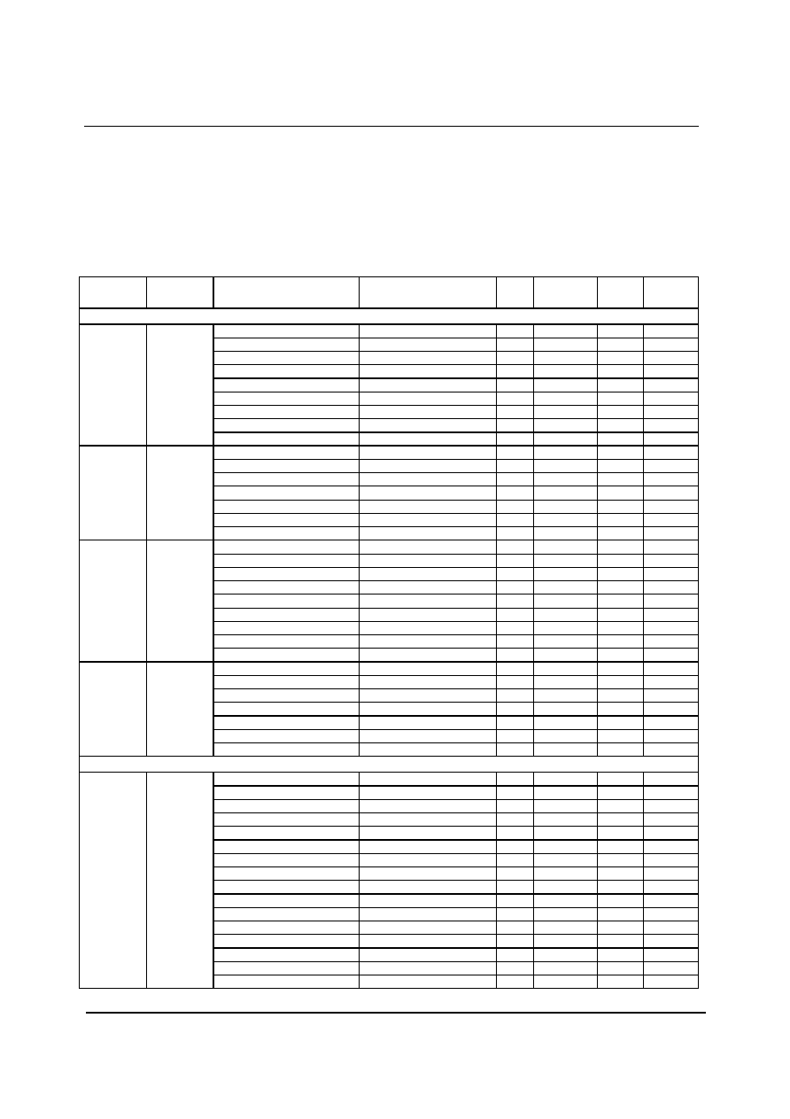
Preliminary Technical Data
WM8972L
w
PTD Rev 2.2 June 2004
33
The clocking of the WM8972L is controlled using the CLKDIV2, USB, and SR control bits. Setting the
CLKDIV2 bit divides MCLK by two internally. The USB bit selects between `Normal' and USB mode.
Each value of SR[4:0] selects one combination of MCLK division ratios and hence one combination
of sample rates (see next page). Since all sample rates are generated by dividing MCLK, their
accuracy depends on the accuracy of MCLK. If MCLK changes, the sample rates change
proportionately.
Note that some sample rates (e.g. 44.1kHz in USB mode) are approximated, i.e. they differ from their
target value by a very small amount. This is not audible, as the maximum deviation is only 0.27%
(8.0214kHz instead of 8kHz in USB mode). By comparison, a half-tone step corresponds to a 5.9%
change in pitch.
MCLK
CLKDIV2=0
MCLK
CLKDIV2=1
ADC SAMPLE RATE
(ADCLRC)
DAC SAMPLE RATE
(DACLRC)
USB
SR [4:0]
FILTER
TYPE
BCLK
(MS=1)
`Normal' Clock Mode (`*' indicates backward compatibility with WM8731)
8 kHz (MCLK/1536)
8 kHz (MCLK/1536)
0
00110 *
1
MCLK/4
8 kHz (MCLK/1536)
48 kHz (MCLK/256)
0
00100 *
1
MCLK/4
12 kHz (MCLK/1024)
12 kHz (MCLK/1024)
0
01000
1
MCLK/4
16 kHz (MCLK/768)
16 kHz (MCLK/768)
0
01010
1
MCLK/4
24 kHz (MCLK/512)
24 kHz (MCLK/512)
0
11100
1
MCLK/4
32 kHz (MCLK/384)
32 kHz (MCLK/384)
0
01100 *
1
MCLK/4
48 kHz (MCLK/256)
8 kHz (MCLK/1536)
0
00010 *
1
MCLK/4
48 kHz (MCLK/256)
48 kHz (MCLK/256)
0
00000 *
1
MCLK/4
12.288 MHz 24.576 MHz
96 kHz (MCLK/128)
96 kHz (MCLK/128)
0
01110 *
3
MCLK/2
8.0182 kHz (MCLK/1408)
8.0182 kHz (MCLK/1408)
0
10110 *
1
MCLK/4
8.0182 kHz (MCLK/1408)
44.1 kHz (MCLK/256)
0
10100 *
1
MCLK/4
11.025 kHz (MCLK/1024)
11.025 kHz (MCLK/1024)
0
11000
1
MCLK/4
22.05 kHz (MCLK/512)
22.05 kHz (MCLK/512)
0
11010
1
MCLK/4
44.1 kHz (MCLK/256)
8.0182 kHz (MCLK/1408)
0
10010 *
1
MCLK/4
44.1 kHz (MCLK/256)
44.1 kHz (MCLK/256)
0
10000 *
1
MCLK/4
11.2896MHz
22.5792MHz
88.2 kHz (MCLK/128)
88.2 kHz (MCLK/128)
0
11110 *
3
MCLK/2
8 kHz (MCLK/2304)
8 kHz (MCLK/2304)
0
00111 *
1
MCLK/6
8 kHz (MCLK/2304)
48 kHz (MCLK/384)
0
00101 *
1
MCLK/6
12 kHz (MCLK/1536)
12 kHz (MCLK/1536)
0
01001
1
MCLK/6
16kHz (MCLK/1152)
16 kHz (MCLK/1152)
0
01011
1
MCLK/6
24kHz (MCLK/768)
24 kHz (MCLK/768)
0
11101
1
MCLK/6
32 kHz (MCLK/576)
32 kHz (MCLK/576)
0
01101 *
1
MCLK/6
48 kHz (MCLK/384)
48 kHz (MCLK/384)
0
00001 *
1
MCLK/6
48 kHz (MCLK/384)
8 kHz (MCLK/2304)
0
00011 *
1
MCLK/6
18.432MHz
36.864MHz
96 kHz (MCLK/192)
96 kHz (MCLK/192)
0
01111 *
3
MCLK/3
8.0182 kHz (MCLK/2112)
8.0182 kHz (MCLK/2112)
0
10111 *
1
MCLK/6
8.0182 kHz (MCLK/2112)
44.1 kHz (MCLK/384)
0
10101 *
1
MCLK/6
11.025 kHz (MCLK/1536)
11.025 kHz (MCLK/1536)
0
11001
1
MCLK/6
22.05 kHz (MCLK/768)
22.05 kHz (MCLK/768)
0
11011
1
MCLK/6
44.1 kHz (MCLK/384)
8.0182 kHz (MCLK/2112)
0
10011 *
1
MCLK/6
44.1 kHz (MCLK/384)
44.1 kHz (MCLK/384)
0
10001 *
1
MCLK/6
16.9344MHz
33.8688MHz
88.2 kHz (MCLK/192)
88.2 kHz (MCLK/192)
0
11111 *
3
MCLK/3
USB Mode (`*' indicates backward compatibility with WM8731)
8 kHz (MCLK/1500)
8 kHz (MCLK/1500)
1
00110 *
0
MCLK
8 kHz (MCLK/1500)
48 kHz (MCLK/250)
1
00100 *
0
MCLK
8.0214 kHz (MCLK/1496)
8.0214kHz (MCLK/1496)
1
10111 *
1
MCLK
8.0214 kHz (MCLK/1496)
44.118 kHz (MCLK/272)
1
10101 *
1
MCLK
11.0259 kHz (MCLK/1088)
11.0259kHz (MCLK/1088)
1
11001
1
MCLK
12 kHz (MCLK/1000)
12 kHz (MCLK/1000)
1
01000
0
MCLK
16kHz (MCLK/750)
16kHz (MCLK/750)
1
01010
0
MCLK
22.0588kHz (MCLK/544)
22.0588kHz (MCLK/544)
1
11011
1
MCLK
24kHz (MCLK/500)
24kHz (MCLK/500)
1
11100
0
MCLK
32 kHz (MCLK/375)
32 kHz (MCLK/375)
1
01100 *
0
MCLK
44.118 kHz (MCLK/272)
8.0214kHz (MCLK/1496)
1
10011 *
1
MCLK
44.118 kHz (MCLK/272)
44.118 kHz (MCLK/272)
1
10001 *
1
MCLK
48 kHz (MCLK/250)
8 kHz (MCLK/1500)
1
00010 *
0
MCLK
48 kHz (MCLK/250)
48 kHz (MCLK/250)
1
00000 *
0
MCLK
88.235kHz (MCLK/136)
88.235kHz (MCLK/136)
1
11111 *
3
MCLK
12.000MHz
24.000MHz
96 kHz (MCLK/125)
96 kHz (MCLK/125)
1
01110 *
2
MCLK
Table 29 Master Clock and Sample Rates
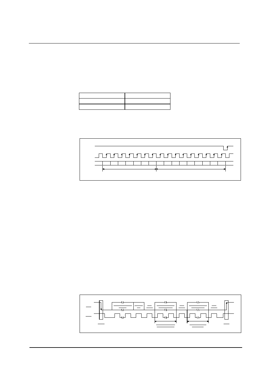
WM8972L
Preliminary Technical Data
w
PTD Rev 2.2 June 2004
34
CONTROL INTERFACE
SELECTION OF CONTROL MODE
The WM8972L is controlled by writing to registers through a serial control interface. A control word
consists of 16 bits. The first 7 bits (B15 to B9) are address bits that select which control register is
accessed. The remaining 9 bits (B8 to B0) are data bits, corresponding to the 9 bits in each control
register. The control interface can operate as either a 3-wire or 2-wire MPU interface. The MODE pin
selects the interface format.
MODE
INTERFACE FORMAT
Low
2 wire
High
3 wire
Table 30 Control Interface Mode Selection
3-WIRE SERIAL CONTROL MODE
In 3-wire mode, every rising edge of SCLK clocks in one data bit from the SDIN pin. A rising edge on
CSB latches in a complete control word consisting of the last 16 bits.
B15
B14
B13
B12
B11
B10
B9
B8
B7
B6
B5
B4
B3
B2
B1
B0
SDIN
SCLK
CSB
control register address
control register data bits
latch
Figure 18 3-Wire Serial Control Interface
2-WIRE SERIAL CONTROL MODE
The WM8972L supports software control via a 2-wire serial bus. Many devices can be controlled by
the same bus, and each device has a unique 7-bit address (this is not the same as the 7-bit address
of each register in the WM8972L).
The WM8972L operates as a slave device only. The controller indicates the start of data transfer with
a high to low transition on SDIN while SCLK remains high. This indicates that a device address and
data will follow. All devices on the 2-wire bus respond to the start condition and shift in the next eight
bits on SDIN (7-bit address + Read/Write bit, MSB first). If the device address received matches the
address of the WM8972L and the R/W bit is `0', indicating a write, then the WM8972L responds by
pulling SDIN low on the next clock pulse (ACK). If the address is not recognised or the R/W bit is `1',
the WM8972L returns to the idle condition and wait for a new start condition and valid address.
Once the WM8972L has acknowledged a correct address, the controller sends the first byte of
control data (B15 to B8, i.e. the WM8972L register address plus the first bit of register data). The
WM8972L then acknowledges the first data byte by pulling SDIN low for one clock pulse. The
controller then sends the second byte of control data (B7 to B0, i.e. the remaining 8 bits of register
data), and the WM8972L acknowledges again by pulling SDIN low.
The transfer of data is complete when there is a low to high transition on SDIN while SCLK is high.
After receiving a complete address and data sequence the WM8972L returns to the idle state and
waits for another start condition. If a start or stop condition is detected out of sequence at any point
during data transfer (i.e. SDIN changes while SCLK is high), the device jumps to the idle condition.
SDIN
SCLK
register address and
1st register data bit
DEVICE ADDRESS
(7 BITS)
RD / WR
BIT
ACK
(LOW)
CONTROL BYTE 1
(BITS 15 TO 8)
CONTROL BYTE 2
(BITS 7 TO 0)
remaining 8 bits of
register data
STOP
START
ACK
(LOW)
ACK
(LOW)
Figure 19 2-Wire Serial Control Interface

Preliminary Technical Data
WM8972L
w
PTD Rev 2.2 June 2004
35
The WM8972L has two possible device addresses, which can be selected using the CSB pin.
CSB STATE
DEVICE ADDRESS
Low
0011010 (0 x 34h)
High
0011011 (0 x 36h)
Table 31 2-Wire MPU Interface Address Selection
POWER SUPPLIES
The WM8972L can use up to four separate power supplies:
∑
AVDD / AGND: Analogue supply, powers all analogue functions except the headphone drivers.
AVDD can range from 1.8V to 3.6V and has the most significant impact on overall power
consumption (except for power consumed in the headphone). A large AVDD slightly improves
audio quality.
∑
OPVDD / OPGND: Output supply, powers the output drivers. OPVDD can range from 1.8V to
3.6V. OPVDD is normally tied to AVDD, but it requires separate layout and decoupling
capacitors to curb harmonic distortion. With a larger OPVDD, louder speaker outputs can be
achieved with lower distortion. If OPVDD is lower than AVDD, the output signal may be clipped.
∑
DCVDD: Digital core supply, powers all digital functions except the audio and control
interfaces. DCVDD can range from 1.42V to 3.6V, and has no effect on audio quality. The
return path for DCVDD is DGND, which is shared with DBVDD.
∑
DBVDD: Digital buffer supply, powers the audio and control interface buffers. This makes it
possible to run the digital core at very low voltages, saving power, while interfacing to other
digital devices using a higher voltage. DBVDD draws much less power than DCVDD, and has
no effect on audio quality. DBVDD can range from 1.8V to 3.6V. The return path for DBVDD is
DGND, which is shared with DCVDD.
It is possible to use the same supply voltage on all four. However, digital and analogue supplies
should be routed and decoupled separately to keep digital switching noise out of the analogue signal
paths.
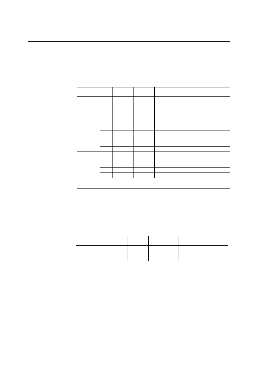
WM8972L
Preliminary Technical Data
w
PTD Rev 2.2 June 2004
36
POWER MANAGEMENT
The WM8972L has two control registers that allow users to select which functions are active. For
minimum power consumption, unused functions should be disabled. To avoid any pop or click noise,
it is important to enable or disable functions in the correct order (see Applications Information).
VMIDSEL is the enable for the Vmid reference, which defaults to disabled and can be enabled as a
50kOhm potential divider or, for low power maintenance of Vref when all other blocks are disabled,
as a 500kOhm potential divider.
REGISTER
ADDRESS
BIT
LABEL
DEFAULT
DESCRIPTION
8:7
VMIDSEL
00
Vmid divider enable and select
00 ≠ Vmid disabled (for OFF mode)
01 ≠ 50kOhm divider enabled (for
playback/record)
10 ≠ 500kOhm divider enabled (for low-power
standby)
11 ≠ 5kOhm divider enabled (for fast start-up)
6
VREF
0
VREF (necessary for all other functions)
5
AIN
0
Analogue in PGA
3
ADC
0
ADC
R25 (19h)
Power
Manageme
nt (1)
1
MICB
0
MICBIAS
8
DAC
0
DAC
4
OUT+
0
OUT+ Output Buffer*
3
OUT-
0
OUT- Output Buffer*
2
MONO
0
MONOOUT Output Buffer and Mono Mixer
R26 (1Ah)
Power
Manageme
nt (2)
1
OUT2
0
OUT2 Output Buffer
Note: All control bits are 0=OFF, 1=ON
* The plus mixer is enabled when OUT+=1. The minus mixer is enabled when OUT-=1.
Table 32 Power Management
STOPPING THE MASTER CLOCK
In order to minimise power consumed in the digital core of the WM8972L, the master clock should be
stopped in Standby and OFF modes. If this is cannot be done externally at the clock source, the
DIGENB bit (R25, bit 0) can be set to stop the MCLK signal from propagating into the device core. In
Standby mode with all supplies at 3.3V, setting DIGENB saves approximately 0.27mA on DCVDD
and 0.2mA on DBVDD. However, since setting DIGENB has no effect on the power consumption of
other system components external to the WM8972L, it is preferable to disable the master clock at its
source wherever possible.
REGISTER
ADDRESS
BIT
LABEL
DEFAULT
DESCRIPTION
R25 (19h)
Additional Control
(1)
1
DIGENB
0
Master clock disable
0: master clock enabled
1: master clock disabled
Table 33 ADC and DAC Oversampling Rate Selection
NOTE: Before DIGENB can be set, the control bits ADC, DAC must be set to zero and a waiting
time of 1ms must be observed. Any failure to follow this procedure may prevent the DAC and
ADC from re-starting correctly.
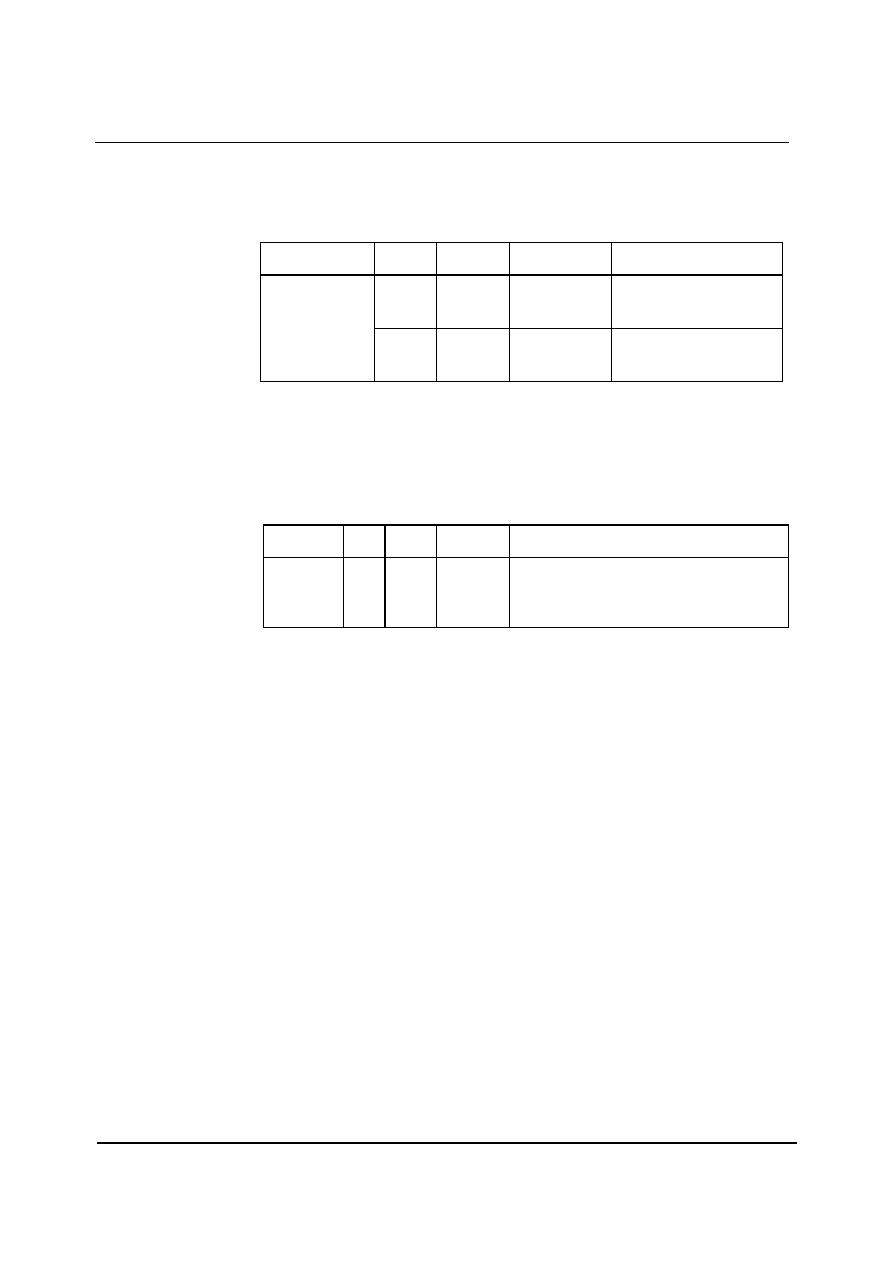
Preliminary Technical Data
WM8972L
w
PTD Rev 2.2 June 2004
37
SAVING POWER BY REDUCING OVERSAMPLING RATE
The default mode of operation of the ADC and DAC digital filters is in 128x oversampling mode.
Under the control of ADCOSR and DACOSR the oversampling rate may be halved. This will result in
a slight decrease in noise performance but will also reduce the power consumption of the device. In
USB mode ADCOSR must be set to 0, i.e. 128x oversampling.
REGISTER
ADDRESS
BIT
LABEL
DEFAULT
DESCRIPTION
1
ADCOSR
0
ADC oversample rate select
1 = 64x (lowest power)
0 = 128x (best SNR)
R24 (18h)
Additional Control
(2)
0
DACOSR
0
DAC oversample rate select
1 = 64x (lowest power)
0 = 128x (best SNR)
Table 34 ADC and DAC Oversampling Rate Selection
ADCOSR set to `1', 64x oversample mode, is not supported in USB mode (USB = 1).
SAVING POWER AT LOW SUPPLY VOLTAGES
The analogue supplies to the WM8972L can run from 1.8V to 3.6V. By default, all analogue circuitry
on the device is optimized to run at 3.3V. This set-up is also good for all other supply voltages down
to 1.8V. However, at lower voltages, it is possible to save power by reducing the internal bias
currents used in the analogue circuitry. This is controlled as shown below.
REGISTER
ADDRESS
BIT
LABEL
DEFAULT
DESCRIPTION
R23 (17h)
Additional
Control(1)
7:6
VSEL
[1:0]
11
Analogue Bias optimization
00: Lowest bias current, optimized for AVDD=1.8V
01: Low bias current, optimized for AVDD=2.5V
1X: Default bias current, optimized for AVDD=3.3V
Note:
In USB mode ADCOSR must be set to 0, i.e. 128x oversampling.
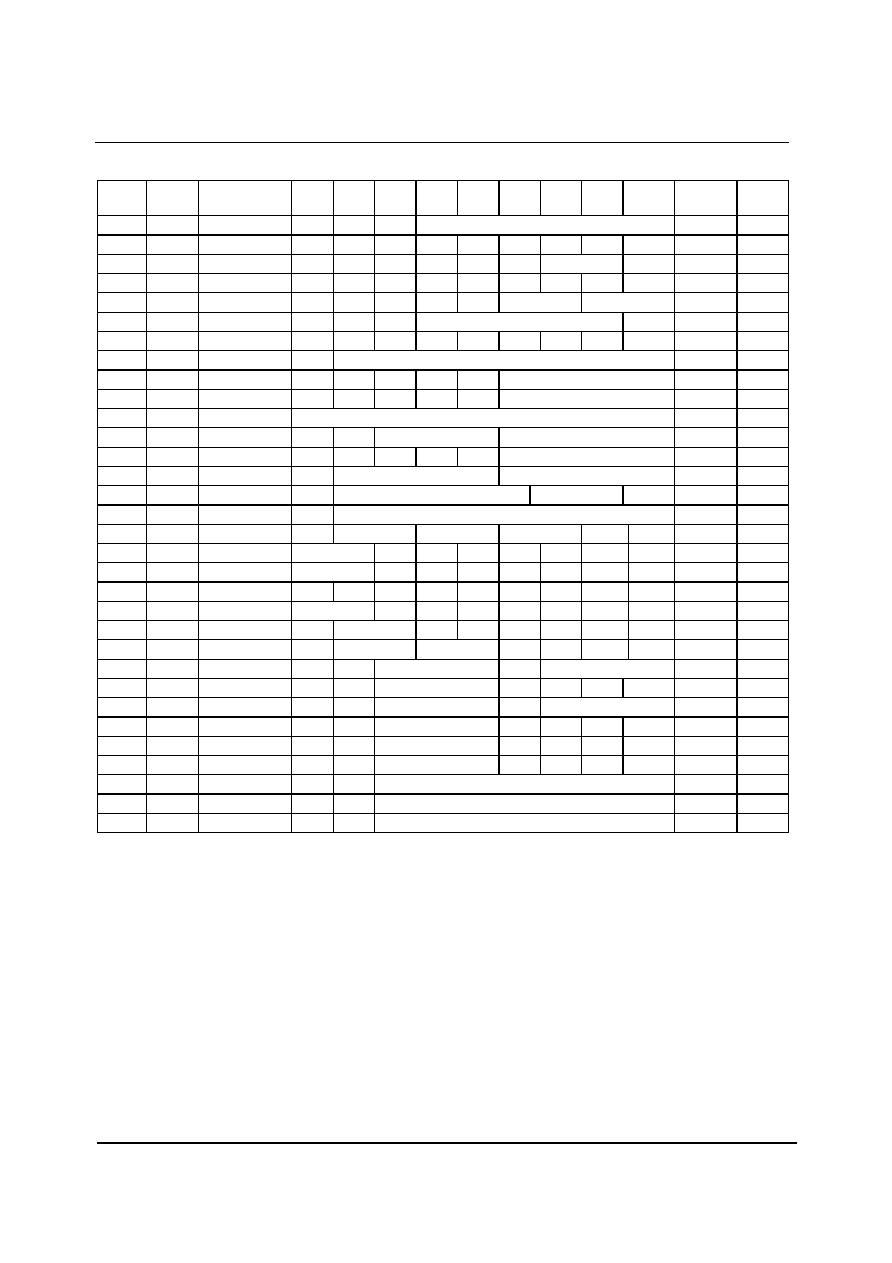
WM8972L
Preliminary Technical Data
w
PTD Rev 2.2 June 2004
38
REGISTER MAP
REGISTER
ADDRESS
(Bit 15 ≠ 9)
remarks
Bit[8]
Bit[7]
Bit[6]
Bit[5]
Bit[4]
Bit[3]
Bit[2]
Bit[1]
Bit[0]
default
page ref
R0 (00h)
0000000
Input volume
IVU
INMUTE
IZC
INVOL
010010111
15
R4 (04h)
0000100
Reserved
0
0
0
0
0
0
0
0
0
000000000
-
R5 (05h)
0000101
ADC & DAC Control ADCDIV2 DACDIV2
0
ADCPOL
HPOR
DACMU
DEEMPH[1:0]
ADCHPD
000001000
15,20,23
R6 (06h)
0000110
Reserved
0
0
0
0
0
0
0
0
0
000000000
-
R7 (07h)
0000111
Audio Interface
0
BCLKINV
MS
0
LRP
WL[1:0]
FORMAT[1:0]
000001010
31
R8 (08h)
0001000
Sample rate
0
0
CLKDIV2
SR[4:0]
USB
000000000
32
R9 (09h)
0001001
Reserved
0
0
0
0
0
0
0
0
0
000000000
-
R10 (0Ah)
0001010
DAC volume
DVU
DACVOL[7:0]
011111111
21
R12 (0Ch)
0001100
Bass control
0
BB
BC
0
0
BASS[3:0]
000001111
22
R13 (0Dh)
0001101
Treble control
0
0
TC
0
0
TRBL[3:0]
000001111
22
R15 (0Fh)
0001111
Reset
writing to this register resets all registers to their default state
not reset
-
R17 (11h)
0010001
ALC1
ALCSEL
0
MAXGAIN[2:0]
ALCL[3:0]
001111011
19
R18 (12h)
0010010
ALC2
0
ALCZC
0
0
0
HLD[3:0]
000000000
19
R19 (13h)
0010011
ALC3
0
DCY[3:0]
ATK[3:0]
000110010
19
R20 (14h)
0010100
Noise Gate
0
NGTH[4:0]
NGG[1:0]
NGAT
000000000
20
R21 (15h)
0010101
ADC volume
AVU
ADCVOL[7:0]
011000011
17
R23 (17h)
0010111
Additional control(1)
TSDEN
VSEL[1:0]
DMONOMIX[1:0]
DATSEL[1:0]
DACINV
TOEN
011000000
14,15,23,27
R24 (18h)
0011000
Additional control(2)
OUT2SW[1:0]
0
0
OUTINV
TRI
LRCM
ADCOSR DACOSR
000000000
27, 27,37
R25 (19h)
0011001
Pwr Mgmt (1)
VMIDSEL[1:0]
VREF
AIN
0
ADC
0
MICB
DIGENB
000000000
36
R26 (1Ah)
0011010
Pwr Mgmt (2)
DAC
0
0
0
OUT+
OUT-
MONO
OUT2
0
000000000
36
R27 (1Bh)
0011011
Additional Control (3)
ADCLRM[1:0]
VROI
0
0
0
0
0
0
000000000
35
R31 (1Fh)
0011111
ADC input mode
DS
MONOMIX[1:0]
0
DCM
0
0
0
0
000000000
14
R32 (20h)
0100000
ADC signal path
0
INSEL[1:0]
MICBOOST[1:0]
0
0
0
0
000000000
14
R34 (22h)
0100010
Plus out Mix (1)
D2+MO +M2+MO
+M2+MOVOL[2:0]
0
+MIXSEL[2:0]
001010000
24
R35 (23h)
0100011
Plus out Mix (2)
0
-M2-MO
-M2-MOVOL[2:0]
0
0
0
0
001010000
24
R36 (24h)
0100100
Minus out Mix (1)
D2-MO +M2-MO
+M2-MOVOL[2:0]
0
-MIXSEL[2:0]
001010000
25
R37 (25h)
0100101
Minus out Mix (2)
0
-M2-MO
-M2-MOVOL[2:0]
0
0
0
0
001010000
25
R38 (26h)
0100110
Mono out Mix (1)
D2MO
+M2MO
+M2MOVOL[2:0]
0
0
0
0
001010000
25
R39 (27h)
0100111
Mono out Mix (2)
0
-M2MO
-M2MOVOL[2:0]
0
0
0
0
001010000
25
R40 (28h)
0101000
OUT+ volume
+OVU
+OZC
+OUTVOL[6:0]
001111001
26
R41 (29h)
0101001
OUT- volume
-OVU
-OZC
-OUTVOL[6:0]
001111001
26
R42 (2Ah)
0101010
MONOOUT volume
0
MOZC
MOUTVOL[6:0]
001111001
26
Note:
All unused register bits must be set to 0.
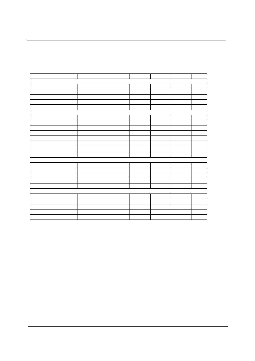
Preliminary Technical Data
WM8972L
w
PTD Rev 2.2 June 2004
39
DIGITAL FILTER CHARACTERISTICS
The ADC and DAC employ different digital filters. There are 4 types of digital filter, called Type 0, 1, 2
and 3. The performance of Types 0 and 1 is listed in the table below, the responses of all filters is
shown in the proceeding pages.
PARAMETER
TEST CONDITIONS
MIN
TYP
MAX
UNIT
ADC Filter Type 0 (USB Mode, 250fs operation)
+/- 0.05dB
0
0.416fs
Passband
-6dB
0.5fs
Passband Ripple
+/- 0.05
dB
Stopband
0.584fs
Stopband Attenuation
f > 0.584fs
-60
dB
ADC Filter Type 1 (USB mode, 272fs or Normal mode operation)
+/- 0.05dB
0
0.4535fs
Passband
-6dB
0.5fs
Passband Ripple
+/- 0.05
dB
Stopband
0.5465fs
Stopband Attenuation
f > 0.5465fs
-60
dB
-3dB
3.7
-0.5dB
10.4
High Pass Filter Corner
Frequency
-0.1dB
21.6
Hz
DAC Filter Type 0 (USB mode, 250fs operation)
+/- 0.03dB
0
0.416fs
Passband
-6dB
0.5fs
Passband Ripple
+/-0.03
dB
Stopband
0.584fs
Stopband Attenuation
f > 0.584fs
-50
dB
DAC Filter Type 1 (USB mode, 272fs or Normal mode operation)
+/- 0.03dB
0
0.4535fs
Passband
-6dB
0.5fs
Passband Ripple
+/- 0.03
dB
Stopband
0.5465fs
Stopband Attenuation
f > 0.5465fs
-50
dB
Table 35 Digital Filter Characteristics
TERMINOLOGY
1.
Stop Band Attenuation (dB) ≠ the degree to which the frequency spectrum is attenuated (outside audio band)
2.
Pass-band Ripple ≠ any variation of the frequency response in the pass-band region
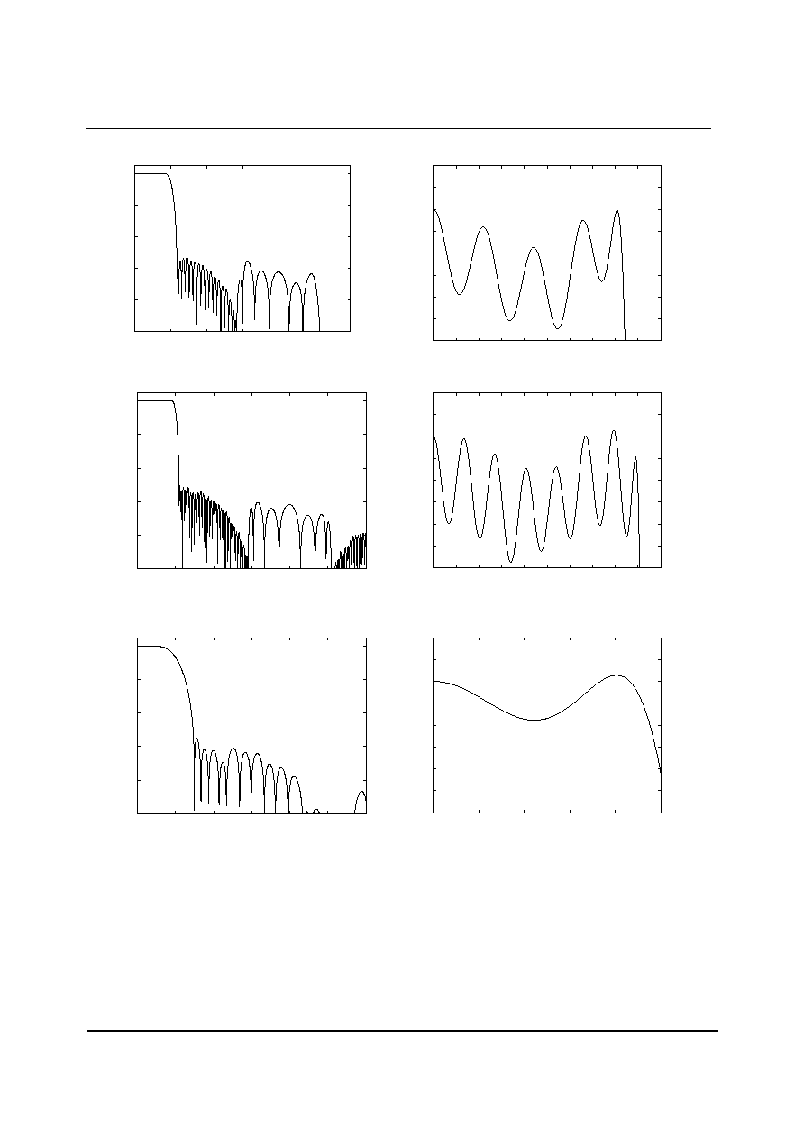
WM8972L
Preliminary Technical Data
w
PTD Rev 2.2 June 2004
40
DAC FILTER RESPONSES
-100
-80
-60
-40
-20
0
0
0.5
1
1.5
2
2.5
3
Response (dB)
Frequency (Fs)
-0.06
-0.05
-0.04
-0.03
-0.02
-0.01
0
0.01
0.02
0
0.05
0.1
0.15
0.2
0.25
0.3
0.35
0.4
0.45
0.5
Response (dB)
Frequency (Fs)
Figure 20 DAC Digital Filter Frequency Response ≠ Type 0 Figure 21 DAC Digital Filter Ripple ≠ Type 0
-100
-80
-60
-40
-20
0
0
0.5
1
1.5
2
2.5
3
Response (dB)
Frequency (Fs)
-0.06
-0.05
-0.04
-0.03
-0.02
-0.01
0
0.01
0.02
0
0.05
0.1
0.15
0.2
0.25
0.3
0.35
0.4
0.45
0.5
Response (dB)
Frequency (Fs)
Figure 22 DAC Digital Filter Frequency Response ≠ Type 1 Figure 23 DAC Digital Filter Ripple ≠ Type 1
-100
-80
-60
-40
-20
0
0
0.5
1
1.5
2
2.5
3
Response (dB)
Frequency (Fs)
-0.06
-0.05
-0.04
-0.03
-0.02
-0.01
0
0.01
0.02
0
0.05
0.1
0.15
0.2
0.25
Response (dB)
Frequency (Fs)
Figure 24 DAC Digital Filter Frequency Response ≠ Type 2 Figure 25 DAC Digital Filter Ripple ≠ Type 2
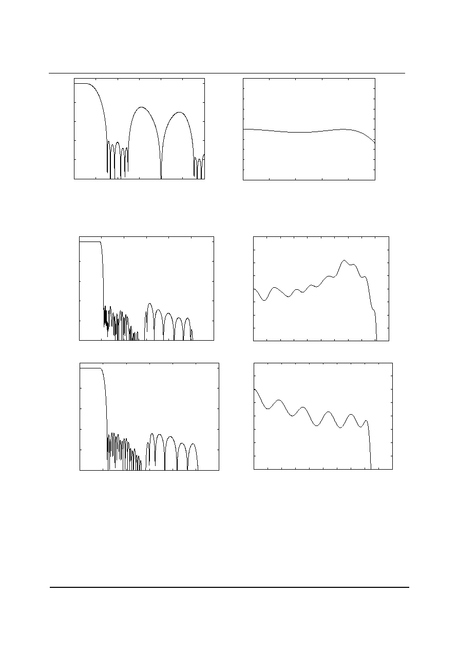
Preliminary Technical Data
WM8972L
w
PTD Rev 2.2 June 2004
41
-100
-80
-60
-40
-20
0
0
0.5
1
1.5
2
2.5
3
Response (dB)
Frequency (Fs)
-0.25
-0.2
-0.15
-0.1
-0.05
0
0.05
0.1
0.15
0.2
0.25
0
0.05
0.1
0.15
0.2
0.25
Response (dB)
Frequency (Fs)
Figure 26 DAC Digital Filter Frequency Response ≠ Type 3 Figure 27 DAC Digital Filter Ripple ≠ Type 3
ADC FILTER RESPONSES
-100
-80
-60
-40
-20
0
0
0.5
1
1.5
2
2.5
3
Response (dB)
Frequency (Fs)
-0.04
-0.03
-0.02
-0.01
0
0.01
0.02
0.03
0.04
0
0.05
0.1
0.15
0.2
0.25
0.3
0.35
0.4
0.45
0.5
Response (dB)
Frequency (Fs)
Figure 28 ADC Digital Filter Frequency Response ≠ Type 0
Figure 29 ADC Digital Filter Ripple ≠ Type 0
-100
-80
-60
-40
-20
0
0
0.5
1
1.5
2
2.5
3
Response (dB)
Frequency (Fs)
-0.06
-0.05
-0.04
-0.03
-0.02
-0.01
0
0.01
0.02
0
0.05
0.1
0.15
0.2
0.25
0.3
0.35
0.4
0.45
0.5
Response (dB)
Frequency (Fs)
Figure 30 ADC Digital Filter Frequency Response ≠ Type 1
Figure 31 ADC Digital Filter Ripple ≠ Type 1
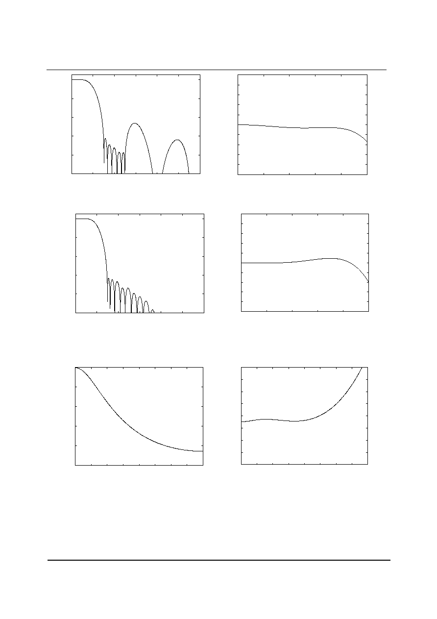
WM8972L
Preliminary Technical Data
w
PTD Rev 2.2 June 2004
42
-100
-80
-60
-40
-20
0
0
0.5
1
1.5
2
2.5
3
Response (dB)
Frequency (Fs)
-0.25
-0.2
-0.15
-0.1
-0.05
0
0.05
0.1
0.15
0.2
0.25
0
0.05
0.1
0.15
0.2
0.25
Response (dB)
Frequency (Fs)
Figure 32 ADC Digital Filter Frequency Response ≠ Type 2 Figure 33 ADC Digital Filter Ripple ≠ Type 2
-100
-80
-60
-40
-20
0
0
0.5
1
1.5
2
2.5
3
Response (dB)
Frequency (Fs)
-0.25
-0.2
-0.15
-0.1
-0.05
0
0.05
0.1
0.15
0.2
0.25
0
0.05
0.1
0.15
0.2
0.25
Response (dB)
Frequency (Fs)
Figure 34 ADC Digital Filter Frequency Response ≠ Type 2 Figure 35 ADC Digital Filter Ripple ≠ Type 3
DE-EMPHASIS FILTER RESPONSES
-10
-8
-6
-4
-2
0
0
2000
4000
6000
8000
10000
12000
14000
16000
Response (dB)
Frequency (Fs)
-0.4
-0.3
-0.2
-0.1
0
0.1
0.2
0.3
0.4
0
2000
4000
6000
8000
10000
12000
14000
16000
Response (dB)
Frequency (Fs)
Figure 36 De-emphasis Frequency Response (32kHz)
Figure 37 De-emphasis Error (32kHz)
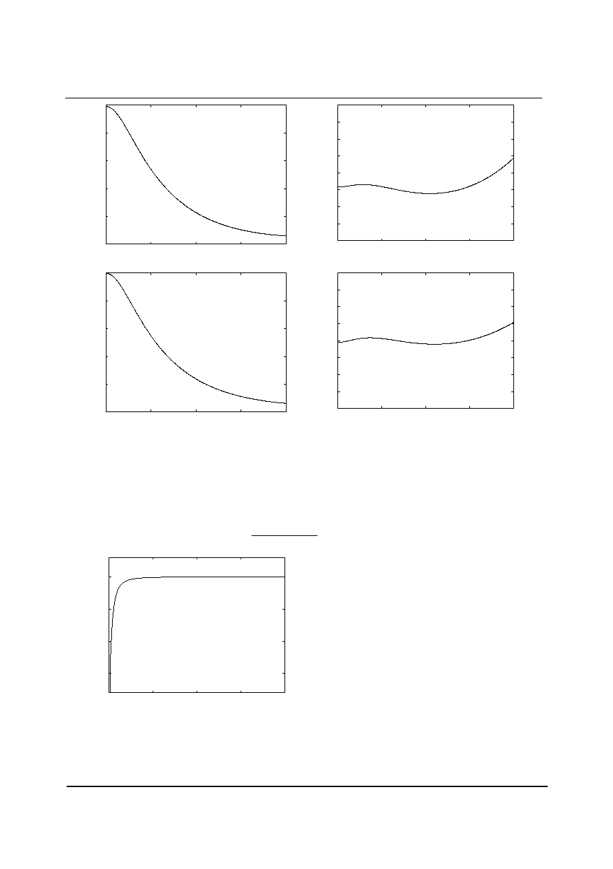
Preliminary Technical Data
WM8972L
w
PTD Rev 2.2 June 2004
43
-10
-8
-6
-4
-2
0
0
5000
10000
15000
20000
Response (dB)
Frequency (Fs)
-0.4
-0.3
-0.2
-0.1
0
0.1
0.2
0.3
0.4
0
5000
10000
15000
20000
Response (dB)
Frequency (Fs)
Figure 38 De-emphasis Frequency Response (44.1kHz)
Figure 39 De-emphasis Error (44.1kHz)
-10
-8
-6
-4
-2
0
0
5000
10000
15000
20000
Response (dB)
Frequency (Fs)
-0.4
-0.3
-0.2
-0.1
0
0.1
0.2
0.3
0.4
0
5000
10000
15000
20000
Response (dB)
Frequency (Fs)
Figure 40 De-emphasis Frequency Response (48kHz)
Figure 41 De-emphasis Error (48kHz)
HIGHPASS FILTER
The WM8972L has a selectable digital highpass filter in the ADC filter path to remove DC offsets. The filter response is
characterised by the following polynomial:
Figure 42 ADC Highpass Filter Response
1 - z
-1
1 - 0.9995z
-1
H(z) =
-15
-10
-5
0
0
0.0005
0.001
0.0015
0.002
Response (dB)
Frequency (Fs)
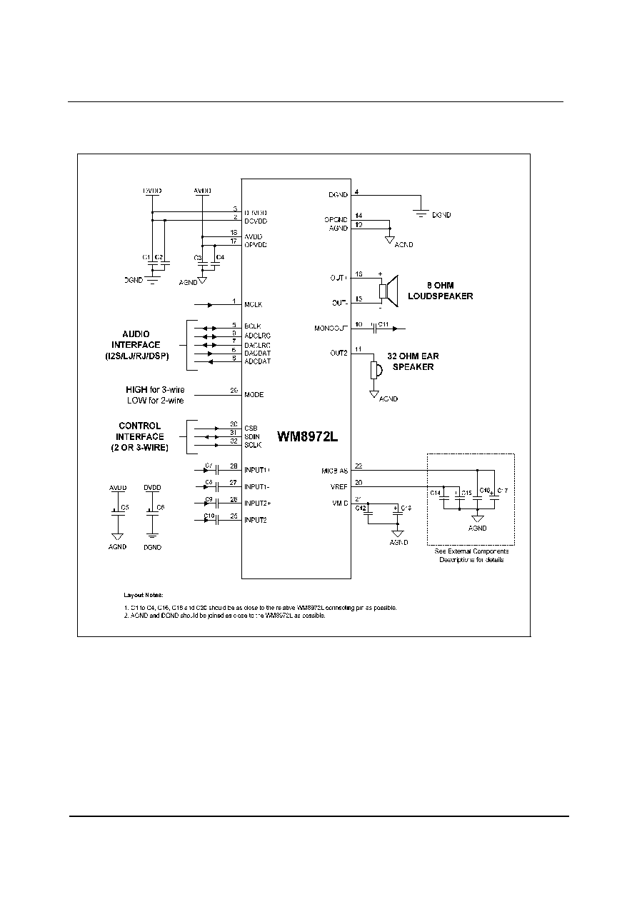
WM8972L
Preliminary Technical Data
w
PTD Rev 2.2 June 2004
44
APPLICATIONS INFORMATION
RECOMMENDED EXTERNAL COMPONENTS
Figure 43 Recommended External Components Diagram
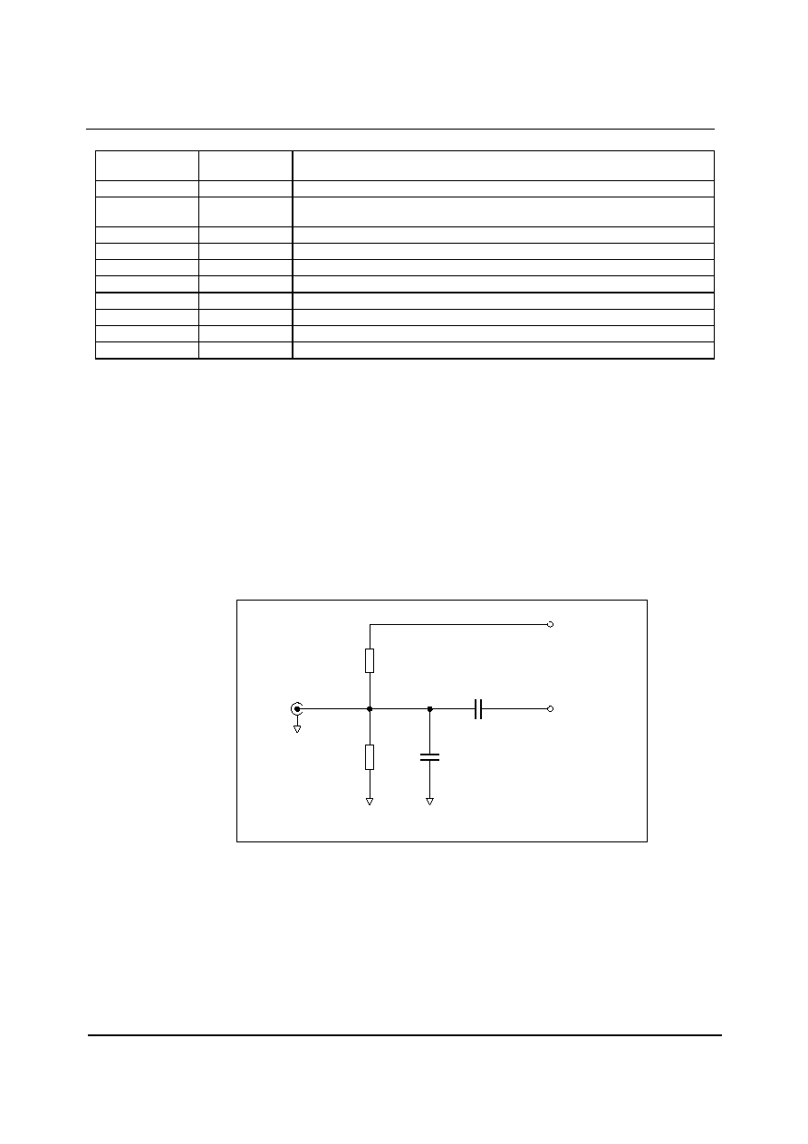
Preliminary Technical Data
WM8972L
w
PTD Rev 2.2 June 2004
45
COMPONENT
REFERENCE
SUGGESTED
VALUE
DESCRIPTION
C1 ≠ C4
100nF
De-coupling for DBVDD, DCVDD, AVDD, OPVDD
C5 ≠ C6
10uF
Reservoir capacitor for DVDD, AVDD. Should the supplies use separate sources then
additional capacitors will be required of each additional source.
C7 ≠ C10
1uF
AC input coupling capacitors
C11
2.2uF
Output AC coupling capacitors to remove DC level from MONOOUT
C12
100nF
De-coupling for VMID.
C13
10uF
Reservoir capacitor for VMID
C14
100nF
De-coupling for VREF
C15
10uF
Reservoir capacitor for VREF
C16
100nF
De-coupling for MICBIAS ≠ Not required if MICBIAS output is not used
C17
10uF
Reservoir capacitor for MICBIAS ≠ Not required if MICBIAS output is not used
Table 36 External Components Descriptions
Note:
1.
For Capacitors C5, C6, C13, C15 and C17 it is recommended that very low ESR components are used.
LINE INPUT CONFIGURATION
When INPUT1+/INPUT1- or INPUT2+/INPUT2- are used as line inputs, the microphone boost and
ALC functions should normally be disabled.
In order to avoid clipping, the user must ensure that the input signal does not exceed AVDD. This
may require a potential divider circuit in some applications. It is also recommended to remove RF
interference picked up on any cables using a simple first-order RC filter, as high-frequency
components in the input signal may otherwise cause aliasing distortion in the audio band. AC signals
with no DC bias should be fed to the WM8972L through a DC blocking capacitor, e.g. 1
µF.
MICROPHONE INPUT CONFIGURATION
Figure 44 Recommended Circuit for Line Input
For interfacing to a microphone, the ALC function should be enabled and the microphone boost
switched on. Microphones held close to a speaker's mouth would normally use the 13dB gain setting,
while tabletop or room microphones would need a 29dB boost.
The recommended application circuit is shown above. R1 and R2 form part of the biasing network
(refer to Microphone Bias section). R1 connected to MICBIAS is necessary only for electret type
microphones that require a voltage bias. R2 should always be present to prevent the microphone
input from charging to a high voltage which may damage the microphone on connection. R1 and R2
should be large so as not to attenuate the signal from the microphone, which can have source
impedance greater than 2kOhm. C1 together with the source impedance of the microphone and the
WM8972L input impedance forms an RF filter. C2 is a DC blocking capacitor to allow the microphone
to be biased at a different DC voltage to the MICIN signal.
R2
47kOhm
C1
220pF
C2
1uF
AGND
AGND
AGND
INPUT1+/-
INPUT2+/-
FROM
MICROPHONE
R1
680 Ohm to 2.2kOhm
check microphone's specification
MICBIAS
WM8972L
Preliminary Technical Data
w
PTD Rev 2.2 June 2004
46
MINIMISING POP NOISE AT THE ANALOGUE OUTPUTS
To minimise any pop or click noise when the system is powered up or down, the following procedures
are recommended.
POWER UP
∑ Switch on power supplies. By default the WM8972L is in Standby Mode, the DAC is
digitally muted and the Audio Interface, Line outputs and Headphone outputs are all OFF
(DACMU = 1 Power Management registers 1 and 2 are all zeros).
∑ Enable Vmid and VREF, then wait for time TBD
∑ Enable DAC as required
∑ Enable line and / or headphone output buffers as required.
∑ Set DACMU = 0 to soft-un-mute the audio DAC.
POWER DOWN
∑ Set DACMU = 1 to soft-mute the audio DAC.
∑ Disable all output buffers, then wait for time TBD.
∑ Switch off the power supplies.
POWER MANAGEMENT EXAMPLES
OPERATION MODE
POWER
MANAGEMENT (1)
POWER
MANAGEMENT (2)
ADC
DAC Output Buffers
VR
E
F
AI
N
MB
I
O2+
O2-
MO
Line-in Record
1
1
1
0
0
0
0
0
Mono Microphone Record
1
1
1
1
0
0
0
0
Microphone to mono out
1
1
0
1
0
0
0
1
Speaker Phone Call [OUTINV = 1]
1
1
0
1
0
1
1
1
Record Phone Call [L channel = mic with
boost, R channel = RX, enable mono mix]
1
1
1
1
0
0
0
1
Table 37 Register Settings for Power Management
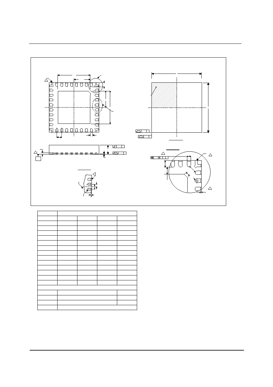
Preliminary Technical Data
WM8972L
w
PTD Rev 2.2 June 2004
47
PACKAGE DIMENSIONS
DM030.C
FL: 32 PIN QFN PLASTIC PACKAGE 5
X
5
X
0.9 mm BODY, 0.50 mm LEAD PITCH
NOTES:
1. DIMENSION b APPLIED TO METALLIZED TERMINAL AND IS MEASURED BETWEEN 0.25 mm AND 0.30 mm FROM TERMINAL TIP. DIMENSION L1 REPRESENTS TERMINAL PULL BACK FROM
PACKAGE SIDE WALL. MAXIMUM OF 0.1mm IS ACCEPTABLE. WHERE TERMINAL PULL BACK EXISTS, ONLY UPPER HALF OF LEAD IS VISIBLE ON PACKAGE SIDE WALL DUE TO HALF
ETCHING OF LEADFRAME.
2. FALLS WITHIN JEDEC, MO-220 WITH THE EXCEPTION OF D2, E2:
D2,E2: LARGER PAD SIZE CHOSEN WHICH IS JUST OUTSIDE JEDEC SPECIFICATION
3. ALL DIMENSIONS ARE IN MILLIMETRES
4. THIS DRAWING IS SUBJECT TO CHANGE WITHOUT NOTICE.
5. SHAPE AND SIZE OF CORNER TIE BAR MAY VARY WITH PACKAGE TERMINAL COUNT. CORNER TIE BAR IS CONNECTED TO EXPOSED PAD INTERNALLY
SEE DETAIL B
E2
E2/2
b
B
16
15
A
8
9
e
5
CORNER
TIE BAR
C
0.08
C
ccc
A
A1
C
(A3)
SEATING PLANE
1
B
D2
L
D2/2
SEE DETAIL A
INDEX AREA
(D/2 X E/2)
TOP VIEW
D
C
aaa
2 X
C
aaa
2 X
E
DETAIL B
T
E
R
M
INAL
T
IP
R
DAT
UM
e
e/
2
L1
1
DETAIL A
B
C
bbb
M
A
32x b
L
32
x
K
L1
R
1
1
0.
56
6 m
m
0.
43
m
m
5
CORNER
TIE BAR
Symbols
Dimensions (mm)
MIN
NOM
MAX
NOTE
A
A1
A3
b
D
D2
E
E2
e
L
L1
R
0.85
0.90
1.00
0.05
0.02
0
0.2 REF
0.30
0.23
0.18
5.00
3.4
3.3
3.2
0.5 BSC
0.35
0.4
0.45
0.1
b(min)/2
1
2
2
1
K
0.20
aaa
bbb
ccc
REF:
0.15
0.10
0.10
JEDEC, MO-220, VARIATION VKKD-2
Tolerances of Form and Position
4.90
5.10
5.00
4.90
5.10
3.4
3.3
3.2
EXPOSED
CENTRE
PAD
1
17
24
25
32

WM8972L
Preliminary Technical Data
w
PTD Rev 2.2 June 2004
48
IMPORTANT NOTICE
Wolfson Microelectronics plc (WM) reserve the right to make changes to their products or to discontinue any product or
service without notice, and advise customers to obtain the latest version of relevant information to verify, before placing
orders, that information being relied on is current. All products are sold subject to the WM terms and conditions of sale
supplied at the time of order acknowledgement, including those pertaining to warranty, patent infringement, and limitation
of liability.
WM warrants performance of its products to the specifications applicable at the time of sale in accordance with WM's
standard warranty. Testing and other quality control techniques are utilised to the extent WM deems necessary to support
this warranty. Specific testing of all parameters of each device is not necessarily performed, except those mandated by
government requirements.
In order to minimise risks associated with customer applications, adequate design and operating safeguards must be used
by the customer to minimise inherent or procedural hazards. Wolfson products are not authorised for use as critical
components in life support devices or systems without the express written approval of an officer of the company. Life
support devices or systems are devices or systems that are intended for surgical implant into the body, or support or
sustain life, and whose failure to perform when properly used in accordance with instructions for use provided, can be
reasonably expected to result in a significant injury to the user. A critical component is any component of a life support
device or system whose failure to perform can be reasonably expected to cause the failure of the life support device or
system, or to affect its safety or effectiveness.
WM assumes no liability for applications assistance or customer product design. WM does not warrant or represent that
any license, either express or implied, is granted under any patent right, copyright, mask work right, or other intellectual
property right of WM covering or relating to any combination, machine, or process in which such products or services might
be or are used. WM's publication of information regarding any third party's products or services does not constitute WM's
approval, license, warranty or endorsement thereof.
Reproduction of information from the WM web site or datasheets is permissible only if reproduction is without alteration and
is accompanied by all associated warranties, conditions, limitations and notices. Representation or reproduction of this
information with alteration voids all warranties provided for an associated WM product or service, is an unfair and deceptive
business practice, and WM is not responsible nor liable for any such use.
Resale of WM's products or services with statements different from or beyond the parameters stated by WM for that
product or service voids all express and any implied warranties for the associated WM product or service, is an unfair and
deceptive business practice, and WM is not responsible nor liable for any such use.
ADDRESS:
Wolfson Microelectronics plc
Westfield House
26 Westfield Road
Edinburgh
EH11 2QB
United Kingdom
Tel :: +44 (0)131 272 7000
Fax :: +44 (0)131 272 7001
Email ::
sales@wolfsonmicro.com
Preliminary Technical Data
WM8972L
w
PTD Rev 2.2 June 2004
49
REVISION HISTORY
DATE
RELEASE
DESCRIPTION OF CHANGES
PAGES
May 2003
Rev 1.0
Created
16 Sept 03
Rev 2.0
Re-created with differential inputs
WM8972LSEFL changed to WM8972LGEFL, /V added to order code and MSL
data changed to MSL3
3
Electrical Characteristics, Input Resistance, DM Measurement added
6
Noise Gate Control note added
21
Audio Interface Diagrams updated,
30-31
Recommended External Components, words 16 or 32 ohm headphones
removed)
45
Power Management Examples updated
47
22 Sept 03
Rev 2.1
Package Drawing updated
48
09 Jun 04
Rev2.2
Order Codes ≠ Peak Soldering Temp added, /V removed and MSL changed to
MSL1
Absolute Maximum Ratings ≠ body temp removed
Speaker Output THD versus Power removed
Package drawing changed
Important notice ≠ address details updated
3
5
8
48
49