Document Outline
- WM8974
- Mono CODEC with Speaker Driver
- DESCRIPTION
- FEATURES
- APPLICATIONS
- TABLE OF CONT NTS
- PIN CONFIGURATION
- ORDERING INFORMATION
- PIN DESCRIPTION
- ABSOLUT MAXIMUM RATINGS
- RECOMMENDED OPERATING CONDITIONS
- ELECTRICAL CHARACTERISTICS
- SIGNAL TIMING REQUIREMENTS
- SYSTEM CLOCK TIMING
- AUDIO INTERFACE TIMING Ö MASTER MODE
- AUDIO INTERFACE TIMING Ö SLAVE MODE
- CONTROL INTERFACE TIMING Ö 3--WIR MODE
- CONTROL INTERFACE TIMING Ö 2--WIR MODE
- DEVICE DESCRIPTION
- INTRODUCTION
- INPUT SIGNAL PATH
- ANALOGUE TO DIGITAL CONVE RTE R (ADC)
- INPUT LIMITER /AUTOMATIC LEVEL CONTROL (ALC)
- OUTPUT SIGNAL PATH
- ANALOGUE OUTPUTS
- OUTPUT SWITCH
- DIGITAL AUDIO INTERFACES
- AUDIO SAMPLE RATES
- MASTER CLOCK AND PHASE LOCKED LOOP (PLL)
- GENERAL PURPOSE INPUT/OUTPUT
- CONTROL INTERFACE
- RESETTING THE CHIP
- POWER SUPPLIES
- POWER MANAGE MENT
- REGISTER MAP
- DIGITAL FILTER CHARACTERISTICS
- TERMINOLOGY
- DAC FILTER RESPONSES
- ADC FILTER RESPONSES
- DE-EMPHASIS FILTER RESPONSES
- HIGHPASS FILTER
- 5-BAND EQUALISER
- APPLICATIONS INFORMATION
- RECOMMENDED EXTERNAL COMPONENTS
- PACKAGE DIAGRAM
- IMPORTANT NOTICE
- ADDRESS

w
WM8974
Mono CODEC with Speaker Driver
WOLFSON MICROELECTRONICS plc
www.wolfsonmicro.com
Product Preview, September 2004, Rev 1.1
Copyright
2004 Wolfson Microelectronics plc
DESCRIPTION
The WM8974 is a low power, high quality mono codec
designed for portable applications such as Digital Still Camera
or Digital Voice Recorder.
The device integrates support for a differential or single ended
mic, and includes drivers for speakers or headphone, and
mono line output. External component requirements are
reduced as no separate microphone or headphone amplifiers
are required.
Advanced Sigma Delta Converters are used along with digital
decimation and interpolation filters to give high quality audio at
sample rates from 8 to 48ks/s. Additional digital filtering
options are available in the ADC path, to cater for application
filtering such as `wind noise reduction', plus an advanced
mixed signal ALC function with noise gate is provided.
An on-chip PLL is provided to generate the required Master
Clock from an external reference clock. The PLL clock can
also be output if required elsewhere in the system.
The WM8974 operates at supply voltages from 2.5 to 3.6V,
although the digital core can operate at voltages down to
1.62V to save power. The speaker and mono outputs use a
separate supply of up to 5V which enables increased output
power if required. Different sections of the chip can also be
powered down under software control by way of the selectable
two or three wire control interface.
WM8974 is supplied in a very small 4x4mm QFN package,
offering high levels of functionality in minimum board area,
with high thermal performance.
FEATURES
∑ Mono Codec:
∑ Audio sample rates:8, 11.025, 16, 22.05, 24, 32, 44.1, 48kHz
∑ DAC SNR 98dB, THD -84dB (`A'-weighted @ 8 ≠ 48ks/s)
∑ ADC SNR 90dB, THD -80dB (`A'-weighted @ 8 ≠ 48ks/s)
∑ On-chip Headphone/Speaker Driver with `cap-less' connect
- 40mW output power into 16
/ 3.3V SPKRVDD
- BTL speaker drive 0.9W into 8
/ 5V SPKRVDD
∑ Additional MONO Line output
∑ Multiple analog or `Aux' inputs, plus analog bypass path
∑ Mic Preamps:
∑ Differential or single end Microphone Interface
- Programmable preamp gain
- Psuedo differential inputs with common mode rejection
- Programmable ALC / Noise Gate in ADC path
∑ Low-noise bias supplied for electret microphones
OTHER FEATURES
∑ 5 band EQ (record or playback path)
∑ Digital Playback Limiter
∑ Programmable ADC High Pass Filter (wind noise reduction)
∑ Programmable ADC Notch Filter
∑ On-chip PLL
∑ Low power, low voltage
- 2.5V to 3.6V (digital core: 1.62V to 3.6V)
- power consumption <10mA all-on 48ks/s mode
∑ 4x4x0.9mm 24 pin QFN package
APPLICATIONS
∑ Digital Still Camera Audio Codec
∑ General Purpose low power audio CODEC

WM8974
Product Preview
w
PP Rev 1.1 September 2004
2
TABLE OF CONTENTS
DESCRIPTION .......................................................................................................1
FEATURES.............................................................................................................1
APPLICATIONS .....................................................................................................1
TABLE OF CONTENTS .........................................................................................2
PIN CONFIGURATION...........................................................................................3
ORDERING INFORMATION ..................................................................................3
ABSOLUTE MAXIMUM RATINGS .........................................................................5
RECOMMENDED OPERATING CONDITIONS .....................................................5
ELECTRICAL CHARACTERISTICS ......................................................................6
TERMINOLOGY ............................................................................................................ 8
SIGNAL TIMING REQUIREMENTS .......................................................................9
SYSTEM CLOCK TIMING ............................................................................................. 9
AUDIO INTERFACE TIMING ≠ MASTER MODE .......................................................... 9
AUDIO INTERFACE TIMING ≠ SLAVE MODE............................................................ 10
CONTROL INTERFACE TIMING ≠ 3-WIRE MODE .................................................... 11
CONTROL INTERFACE TIMING ≠ 2-WIRE MODE .................................................... 12
DEVICE DESCRIPTION .......................................................................................13
INTRODUCTION ......................................................................................................... 13
INPUT SIGNAL PATH ................................................................................................. 14
ANALOGUE TO DIGITAL CONVERTER (ADC).......................................................... 19
INPUT LIMITER / AUTOMATIC LEVEL CONTROL (ALC) .......................................... 22
OUTPUT SIGNAL PATH ............................................................................................. 26
ANALOGUE OUTPUTS............................................................................................... 33
OUTPUT SWITCH ...................................................................................................... 38
DIGITAL AUDIO INTERFACES................................................................................... 40
AUDIO SAMPLE RATES ............................................................................................. 46
MASTER CLOCK AND PHASE LOCKED LOOP (PLL) ............................................... 47
GENERAL PURPOSE INPUT/OUTPUT...................................................................... 49
CONTROL INTERFACE.............................................................................................. 49
RESETTING THE CHIP........................................................................................50
POWER SUPPLIES .................................................................................................... 50
POWER MANAGEMENT ............................................................................................ 51
REGISTER MAP...................................................................................................52
DIGITAL FILTER CHARACTERISTICS ...............................................................53
TERMINOLOGY .......................................................................................................... 53
DAC FILTER RESPONSES .................................................................................54
ADC FILTER RESPONSES .................................................................................54
DE-EMPHASIS FILTER RESPONSES ................................................................55
HIGHPASS FILTER..............................................................................................56
5-BAND EQUALISER...........................................................................................57
APPLICATIONS INFORMATION .........................................................................61
RECOMMENDED EXTERNAL COMPONENTS .......................................................... 61
PACKAGE DIAGRAM ..........................................................................................62
IMPORTANT NOTICE ..........................................................................................63
ADDRESS ................................................................................................................... 63

Product Preview
WM8974
w
PP Rev 1.1 September 2004
3
PIN CONFIGURATION
ORDERING INFORMATION
ORDER CODE
TEMPERATURE
RANGE
PACKAGE
MOISTURE SENSITIVITY
LEVEL
PACKAGE BODY
TEMPERATURE
WM8974GEFL/V
-25
∞C to +85∞C
(lead free)
24-pin QFN (4x4x0.9mm)
MSL3
260
o
C
WM8974GEFL/RV
-25
∞C to +85∞C
(lead free,
tape and reel)
24-pin QFN (4x4x0.9mm)
MSL3
260
o
C
Note:
Reel Quantity = 3,500

WM8974
Product Preview
w
PP Rev 1.1 September 2004
4
PIN DESCRIPTION
PIN NO
NAME
TYPE
DESCRIPTION
1
MICBIAS
Analogue Output
Microphone Bias
2
AVDD
Supply
Analogue supply (feeds ADC and DAC)
3
AGND
Supply
Analogue ground (feeds ADC and DAC)
4
DCVDD
Supply
Digital Core supply
5
DBVDD
Supply
Digital Buffer (Input/Output) supply
6
DGND
Supply
Digital ground
7
ADCDAT
Digital Output
ADC Digital Audio Data Output
8
DACDAT
Digital Input
DAC Digital Audio Data Input
9
FRAME
Digital Input / Output
DAC and ADC Sample Rate Clock or Frame synch
10
BCLK
Digital Input / Output
Digital Audio Port Clock
11
MCLK
Digital Input
Master Clock Input
12
CSB/GPIO
Digital Input / Output
3-Wire MPU Chip Select or General Purpose Input/Output pin.
13
SCLK
Digital Input
3-Wire MPU Clock Input / 2-Wire MPU Clock Input
14
SDIN
Digital Input / Output
3-Wire MPU Data Input / 2-Wire MPU Data Input
15
MODE
Digital Input
Control Interface Mode Selection Pin.
16
MONOOUT
Analogue Output
mono output
17
SPKROUTP
Analogue Output
Speaker Output Positive
18
SPKRGND
Supply
Speaker ground (feeds speaker and mono output amps only)
19
SPKROUTN
Analogue Output
Speaker Output Negative
20
SPKRVDD
Supply
Speaker supply (feeds speaker and mono output amps only)
21
AUX
Analogue Input
Auxiliary analogue input
22
VMID
Reference
Decoupling for midrail reference voltage
23
MICN
Analogue Input
Microphone negative input
24
MICP
Analogue Input
Microphone positive input (common mode)

Product Preview
WM8974
w
PP Rev 1.1 September 2004
5
ABSOLUTE MAXIMUM RATINGS
Absolute Maximum Ratings are stress ratings only. Permanent damage to the device may be caused by continuously
operating at or beyond these limits. Device functional operating limits and guaranteed performance specifications are given
under Electrical Characteristics at the test conditions specified.
ESD Sensitive Device. This device is manufactured on a CMOS process. It is therefore generically susceptible to
damage from excessive static voltages. Proper ESD precautions must be taken during handling and storage of this
device.
Wolfson tests its package types according to IPC/JEDEC J-STD-020B for Moisture Sensitivity to determine acceptable storage
conditions prior to surface mount assembly. These levels are:
MSL1 = unlimited floor life at <30
∞C / 85% Relative Humidity. Not normally stored in moisture barrier bag.
MSL2 = out of bag storage for 1 year at <30
∞C / 60% Relative Humidity. Supplied in moisture barrier bag.
MSL3 = out of bag storage for 168 hours at <30
∞C / 60% Relative Humidity. Supplied in moisture barrier bag.
The Moisture Sensitivity Level for each package type is specified in Ordering Information.
CONDITION
MIN
MAX
DBVDD, DCVDD, AVDD supply voltages
-0.3V
+3.63V
SPKRVDD supply voltage
-0.3V
+7V
Voltage range digital inputs
DGND -0.3V
DVDD +0.3V
Voltage range analogue inputs
AGND -0.3V
AVDD +0.3V
Operating temperature range, T
A
-25
∞C
+85
∞C
Storage temperature prior to soldering
30
∞C max / 85% RH max
Storage temperature after soldering
-65
∞C
+150
∞C
Notes
1.
Analogue and digital grounds must always be within 0.3V of each other.
2.
All digital and analogue supplies are completely independent from each other.
RECOMMENDED OPERATING CONDITIONS
PARAMETER
SYMBOL
TEST CONDITIONS
MIN
TYP
MAX
UNIT
Digital supply range (Core)
DCVDD
1.62
3.6
V
Digital supply range (Buffer)
DBVDD
2.5
3.6
V
Analogue supplies range
AVDD
2.5
3.6
V
Speaker supply
SPKRVDD
2.5
5.5
V
Ground
DGND,AGND,
SPKRGND
0
V
WM8974
Product Preview
w
PP Rev 1.1 September 2004
6
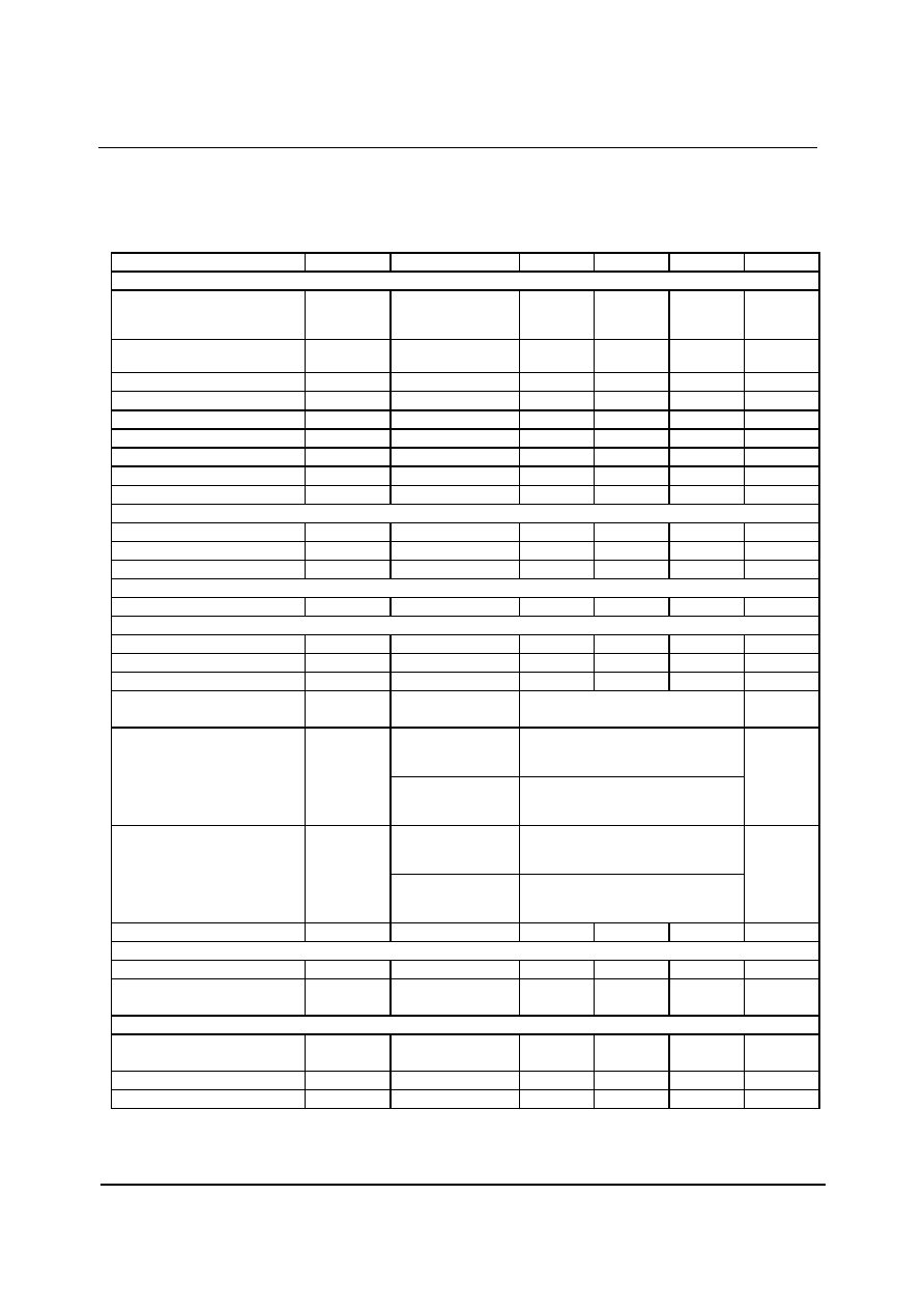
ELECTRICAL CHARACTERISTICS
Test Conditions
DCVDD = 1.62V, AVDD = DBVDD = 3.3V, DBVDD = 3.3V, T
A
= +25
o
C, 1kHz signal, fs = 48kHz, 24-bit audio data unless
otherwise stated.
PARAMETER
SYMBOL
TEST CONDITIONS
MIN
TYP
MAX
UNIT
Microphone Inputs (MICN, MICP)
Full-scale Input Signal Level
(Note 1) ≠ note this changes with
AVDD
V
INFS
PGABOOST = 0dB
INPPGAVOL = 0dB
1.0
0
V rms
dBV
Mic PGA equivalent input noise
At 35.25dB
gain
TBD
uV
Input resistance
R
MICIN
Gain set to 35.25dB
1.6
k
Input resistance
R
MICIN
Gain set to 0dB
47
k
Input resistance
R
MICIN
Gain set to -12dB
75
k
Input resistance
R
MICIP
MICP2INPPGA = 1
94
k
Input resistance
R
MICIP
MICP2INPPGA = 0
TBD
k
Input Capacitance
C
MICIN
10
pF
Recommended coupling cap
C
COUP
220
pF
MIC Input Programmable Gain Amplifier (PGA)
Programmable Gain
-12
35.25
dB
Programmable Gain Step Size
Guaranteed monotonic
0.75
dB
Mute Attenuation
TBD
dB
Selectable Input Gain Boost (0/+20dB)
Gain Boost
0
20
dB
Automatic Level Control (ALC)/Limiter ≠ ADC only
Target Record Level
-28.5
-6
dB
Programmable Gain
-12
35.25
dB
Programmable Gain Step Size
Guaranteed Monotonic
0.75
dB
Gain Hold Time (Note 2)
t
HOLD
MCLK=12.288MHz
(Note 4)
0, 2.67, 5.33, 10.67, ... , 43691
(time doubles with each step)
ms
ALCMODE=0 (ALC),
MCLK=12.288MHz
(Note 4)
3.3, 6.6, 13.1, ... , 3360
(time doubles with each step)
Gain Ramp-Up (Decay) Time
(Note 3)
t
DCY
ALCMODE=1 (limiter),
MCLK=12.288MHz
(Note 4)
0.73, 1.45, 2.91, ... , 744
(time doubles with each step)
ms
ALCMODE=0 (ALC),
MCLK=12.288MHz
(Note 4)
0.83, 1.66, 3.33, ... , 852
(time doubles with each step)
Gain Ramp-Down (Attack) Time
(Note 3)
t
ATK
ALCMODE=1 (limiter),
MCLK=12.288MHz
(Note 4)
0.18, 0.36, 0.73, ... , 186
(time doubles with each step)
ms
Mute Attenuation
TBD
dB
Analogue to Digital Converter (ADC)
Signal to Noise Ratio (Note 5, 6)
A-weighted, 0dB gain
90
dB
Total Harmonic Distortion
(Note 7)
full-scale, 0dB gain
-80
dB
Auxilliary Analogue Input (AUX)
Full-scale Input Signal Level (0dB)
≠ note this changes with AVDD
V
INFS
1.0
0
V rms
dBV
Input Resistance
R
AUXIN
AUXMODE=0
20
k
Input Capacitance
C
AUXIN
10
pF

Product Preview
WM8974
w
PP Rev 1.1 September 2004
7
Test Conditions
DCVDD = 1.62V, AVDD = DBVDD = 3.3V, TA = +25
o
C, 1kHz signal, fs = 48kHz, 24-bit audio data unless otherwise stated.
PARAMETER
SYMBOL
TEST CONDITIONS
MIN
TYP
MAX
UNIT
Digital to Analogue Converter (DAC) to MONO output (all data measured with 10k
/ 50pF load)
Signal to Noise Ratio (Note 5)
SNR
A-weighted
TBD
98
dB
Total Harmonic Distortion
(Note 7)
THD
R
L
= 10 k
full-scale signal
-84
dB
MONOBOOST=0
AVDD/3.3
0dB Full Scale output voltage
(Note 9)
MONOBOOST=1
1.5x
(AVDD/3.3)
V
RMS
Speaker Output PGA
Programmable Gain
-57
6
dB
Programmable Gain Step Size
Guaranteed monotonic
1
dB
BTL Speaker Output (SPKROUTP, SPKROUTN with 8
bridge tied load)
Output Power
P
O
Output power is very closely correlated with THD; see below
P
O
=180mW, R
L
= 8
,
SPKRVDD=3.3V
0.3
-50
%
dB
P
O
=400mW, R
L
= 8
,
SPKRVDD=3.3V
1.0
-40
%
dB
P
O
=360mW, R
L
= 8
,
SPKRVDD=5V
0.3
-50
%
dB
Total Harmonic Distortion
THD
P
O
=800mW, R
L
= 8
,
SPKRVDD=5V
1
-40
%
dB
SPKRVDD=3.3V,
R
L
= 8
90
dB
Signal to Noise Ratio
SNR
SPKRVDD=5V,
R
L
= 8
90
dB
Power Supply Rejection Ratio
50
dB
`Headphone' output (SPKROUTP, SPKROUTN with resistive load to ground)
Signal to Noise Ratio
SNR
93
dB
Total Harmonic Distortion
THD
Po=20mW, R
L
= 16
,
SPKRVDD=3.3V
0.008
-81
%
dB
Po=20mW, R
L
= 32
,
SPKRVDD=3.3V
0.007
- 83
%
dB
Microphone Bias
Bias Voltage (MBVSEL=0)
V
MICBIAS
0.9*AVDD
V
Bias Voltage (MBVSEL=1)
V
MICBIAS
0.75*AVDD
V
Bias Current Source
I
MICBIAS
3
mA
Output Noise Voltage
Vn
1K to 20kHz
15
nV/
Hz
Digital Input / Output
Input HIGH Level
V
IH
0.7
◊DVDD
V
Input LOW Level
V
IL
0.3
◊DVDD
V
Output HIGH Level
V
OH
I
OL
=1mA
0.9
◊DVDD
V
Output LOW Level
V
OL
I
OH
-1mA
0.1xDVDD
V

WM8974
Product Preview
w
PP Rev 1.1 September 2004
8
TERMINOLOGY
1.
MICN input only in single ended microphone configuration. Maximum input signal to MICP without distortion is -3dBV.
2.
Hold Time is the length of time between a signal detected being too quiet and beginning to ramp up the gain. It does
not apply to ramping down the gain when the signal is too loud, which happens without a delay.
3.
Ramp-up and Ramp-Down times are defined as the time it takes for the PGA to change it's gain by 6dB.
4.
All hold, ramp-up and ramp-down times scale proportionally with MCLK
5.
Signal-to-noise ratio (dB) ≠ SNR is a measure of the difference in level between the full scale output and the output with
no signal applied. (No Auto-zero or Automute function is employed in achieving these results).
6.
THD+N (dB) ≠ THD+N is a ratio, of the rms values, of (Noise + Distortion)/Signal.
7.
The maximum output voltage can be limited by the speaker power supply. If MONOBOOST=1 then SPKVDD should
be 1.5xAVDD or higher to prevent clipping taking place in the output stage.

Product Preview
WM8974
w
PP Rev 1.1 September 2004
9
SIGNAL TIMING REQUIREMENTS
SYSTEM CLOCK TIMING
MCLK
t
MCLKL
t
MCLKH
t
MCLKY
Figure 1 System Clock Timing Requirements
Test Conditions
DCVDD=1.62V, DBVDD=AVDD=SPKRVDD=3.3V, DGND=AGND=SPKRGND=0V, T
A
= +25
o
C, Slave Mode fs = 48kHz, MCLK =
256fs, 24-bit data, unless otherwise stated.
PARAMETER
SYMBOL
MIN
TYP
MAX
UNIT
System Clock Timing Information
MCLK System clock cycle time
T
MCLKY
Tbd
ns
MCLK duty cycle
T
MCLKDS
60:40
40:60
AUDIO INTERFACE TIMING ≠ MASTER MODE
Figure 2 Digital Audio Data Timing ≠ Master Mode (see Control Interface)

WM8974
Product Preview
w
PP Rev 1.1 September 2004
10
Test Conditions
DCVDD=1.62V, DBVDD=AVDD=SPKRVDD=3.3V, DGND=AGND=SPKRGND=0V, T
A
=+25
o
C, Slave Mode, fs=48kHz,
MCLK=256fs, 24-bit data, unless otherwise stated.
PARAMETER
SYMBOL
MIN
TYP
MAX
UNIT
Audio Data Input Timing Information
FRAME propagation delay from BCLK falling edge
t
DL
10
ns
ADCDAT propagation delay from BCLK falling edge
t
DDA
10
ns
DACDAT setup time to BCLK rising edge
t
DST
10
ns
DACDAT hold time from BCLK rising edge
t
DHT
10
ns
AUDIO INTERFACE TIMING ≠ SLAVE MODE
Figure 3 Digital Audio Data Timing ≠ Slave Mode
Test Conditions
DCVDD=1.62V, DBVDD=AVDD=SPKRVDD=3.3V, DGND=AGND=SPKRGND=0V, T
A
=+25
o
C, Slave Mode, fs=48kHz, MCLK=
256fs, 24-bit data, unless otherwise stated.
PARAMETER
SYMBOL
MIN
TYP
MAX
UNIT
Audio Data Input Timing Information
BCLK cycle time
t
BCY
50
ns
BCLK pulse width high
t
BCH
20
ns
BCLK pulse width low
t
BCL
20
ns
FRAME set-up time to BCLK rising edge
t
LRSU
10
ns
FRAME hold time from BCLK rising edge
t
LRH
10
ns
DACDAT hold time from BCLK rising edge
t
DH
10
ns
ADCDAT propagation delay from BCLK falling edge
t
DD
10
ns
Note:
BCLK period should always be greater than or equal to MCLK period.

Product Preview
WM8974
w
PP Rev 1.1 September 2004
11
CONTROL INTERFACE TIMING ≠ 3-WIRE MODE
Figure 4 Control Interface Timing ≠ 3-Wire Serial Control Mode
Test Conditions
DCVDD = 1.62V, DBVDD = AVDD = SPKRVDD = 3.3V, DGND = AGND = SPKRGND = 0V, T
A
= +25
o
C, Slave Mode, fs =
48kHz, MCLK = 256fs, 24-bit data, unless otherwise stated.
PARAMETER
SYMBOL
MIN
TYP
MAX
UNIT
Program Register Input Information
SCLK rising edge to CSB rising edge
t
SCS
80
ns
SCLK pulse cycle time
t
SCY
200
ns
SCLK pulse width low
t
SCL
80
ns
SCLK pulse width high
t
SCH
80
ns
SDIN to SCLK set-up time
t
DSU
40
ns
SCLK to SDIN hold time
t
DHO
40
ns
CSB pulse width low
t
CSL
40
ns
CSB pulse width high
t
CSH
40
ns
CSB rising to SCLK rising
t
CSS
40
ns
Pulse width of spikes that will be suppressed
t
ps
0
5
ns
WM8974
Product Preview
w
PP Rev 1.1 September 2004
12
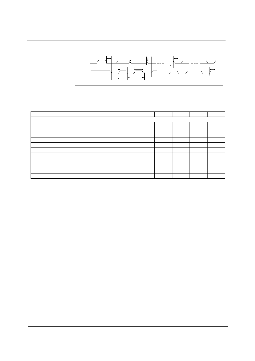
CONTROL INTERFACE TIMING ≠ 2-WIRE MODE
SDIN
SCLK
t
3
t
1
t
6
t
2
t
7
t
5
t
4
t
3
t
8
t
9
Figure 5 Control Interface Timing ≠ 2-Wire Serial Control Mode
Test Conditions
DCVDD=1.62V, DBVDD=AVDD=SPKRVDD=3.3V, DGND=AGND=SPKRGND=0V, T
A
= +25
o
C, Slave Mode, fs = 48kHz, MCLK
= 256fs, 24-bit data, unless otherwise stated.
PARAMETER
SYMBOL
MIN
TYP
MAX
UNIT
Program Register Input Information
SCLK Frequency
0
400
kHz
SCLK Low Pulse-Width
t
1
600
ns
SCLK High Pulse-Width
t
2
1.3
us
Hold Time (Start Condition)
t
3
600
ns
Setup Time (Start Condition)
t
4
600
ns
Data Setup Time
t
5
100
ns
SDIN, SCLK Rise Time
t
6
300
ns
SDIN, SCLK Fall Time
t
7
300
ns
Setup Time (Stop Condition)
t
8
600
ns
Data Hold Time
t
9
900
ns
Pulse width of spikes that will be suppressed
t
ps
0
5
ns

Product Preview
WM8974
w
PP Rev 1.1 September 2004
13
DEVICE DESCRIPTION
INTRODUCTION
The WM8974 is a low power audio codec combining a high quality mono audio DAC and ADC, with
flexible line and microphone input and output processing. Applications for this device are anticipated
to include digital still cameras with mono audio, record and playback capability and also voice
recorders.
FEATURES
The chip offers great flexibility in use, and so can support many different modes of operation as
follows:
MICROPHONE INPUTS
Two microphone inputs are provided, allowing for either a differential microphone input or a single
ended microphone to be connected. These inputs have a user programmable gain range of -12dB
to +35.25dB using internal resistors. After the input PGA stage comes a boost stage which can add
a further 20dB of gain. A microphone bias is output from the chip which can be used to bias the
microphones. The signal routing can be configured to allow manual adjustment of mic levels, or to
allow the ALC loop to control the level of mic signal that is transmitted.
Total gain through the microphone paths of up to +55.25dB can be selected.
PGA AND ALC OPERATION
A programmable gain amplifier is provided in the input path to the ADC. This may be used manually
or in conjunction with a mixed analogue/digital automatic level control (ALC) which keeps the
recording volume constant.
AUX INPUT
The device includes a mono input, AUX, that can be used as an input for warning tones (beep) etc.
The output from this circuit can be summed into the mono output and/or the speaker output paths,
so allowing for mixing of audio with `backing music' etc as required. This path can also be summed
into the input in a flexible fashion, either to the input PGA as a second microphone input or as a line
input. The configuration of this circuit, with integrated on-chip resistors allows several analogue
signals to be summed into the single AUX input if required.
ADC
The mono ADC uses a multi-bit high-order oversampling architecture to deliver optimum
performance with low power consumption. Various sample rates are supported, from the 8ks/s rate
typically used in voice dictation, up to the 48ks/s rate used in high quality audio applications.
Hi-Fi DAC
The hi-fi DAC provides high quality audio playback suitable for all portable mono audio type
applications.
DIGITAL FILTERING
Advanced Sigma Delta Converters are used along with digital decimation and interpolation filters to
give high quality audio at sample rates from 8ks/s to 48ks/s.
Application specific digital filters are also available which help to reduce the effect of specific noise
sources such as `wind noise'. The filters include a programmable ADC high pass filter, a
programmable ADC notch filter and a 5-band equaliser that can be applied to either the ADC or the
DAC path in order to improve the overall audio sound from the device.
OUTPUT MIXING AND VOLUME ADJUST
Flexible mixing is provided on the outputs of the device; a mixer is provided for the speaker outputs,
and an additional mono summer for the mono output. These mixers allow the output of the DAC, the
output of the ADC volume control and the Auxilliary input to be combined. The output volume can
be adjusted using the integrated digital volume control and there is additional analogue gain
adjustment capability on the speaker output.
AUDIO INTERFACES
The WM8974 has a standard audio interface, to support the transmission of audio data to and from
the chip. This interface is a 4 wire standard audio interface which supports a number of audio data
formats including I
2
S, DSP Mode, MSB-First, left justified and MSB-First, right justified, and can
operate in master or slave modes.

WM8974
Product Preview
w
PP Rev 1.1 September 2004
14
CONTROL INTERFACES
To allow full software control over all its features, the WM8974 offers a choice of 2 or 3 wire MPU
control interface. It is fully compatible and an ideal partner for a wide range of industry standard
microprocessors, controllers and DSPs. The selection between 2-wire mode and 3-wire mode is
determined by the state of the MODE pin. If MODE is high then 3-wire control mode is selected, if
MODE is low then 2-wire control mode is selected.
In 2 wire mode, only slave operation is supported, and the address of the device is fixed as 0011010.
CLOCKING SCHEMES
WM8974 offers the normal audio DAC clocking scheme operation, where 256fs MCLK is provided to
the DAC/ADC.
However, a PLL is also included which may be used to generate the internal master clock frequency
in the event that this is not available from the system controller. This PLL uses an input clock,
typically the 12MHz USB or ilink clock, to generate high quality audio clocks. If this PLL is not
required for generation of these clocks, it can be reconfigured to generate alternative clocks which
may then be output on the CSB/GPIO pin and used elsewhere in the system.
POWER CONTROL
The design of the WM8974 has given much attention to power consumption without compromising
performance. It operates at low supply voltages, and includes the facility to power off any unused
parts of the circuitry under software control, includes standby and power off modes.
INPUT SIGNAL PATH
The WM8974 has 3 flexible analogue inputs: two microphone inputs, and an auxiliary input. These
inputs can be used in a variety of ways. The input signal path before the ADC has a flexible PGA
block which then feeds into a gain boost/mixer stage.
MICROPHONE INPUTS
The WM8974 can accommodate a variety of microphone configurations including single ended and
differential inputs. The inputs through the MICN, MICP and optionally AUX pins are amplified
through the input PGA as shown in Figure 6.
A differential input is the preferential configuration where the positive terminal of the input PGA is
connected to the MICP input pin by setting MICP2INPPGA=1. The other microphone terminal should
then be connected to MICN (when MICN2INPPGA=1) or optionally to AUX (when AUX2INPPGA=1)
input pins.
Single ended microphone inputs should connect to the MICP input with MICP2INPPGA set to 1. The
negative terminal of the input PGA should be connected to VMID externally through a cap. This is
achieved by setting register bit MICN2INPPGA=1.
Alternatively a single ended microphone can be connected to the MICN input with MICN2INPPGA set
to 1. The positive terminal of the input PGA should be connected internally to VMID by setting
MICP2INPPGA to 0.

Product Preview
WM8974
w
PP Rev 1.1 September 2004
15
Figure 6 Microphone Input PGA Circuit
(switch positions shown are for differential mic input)
REGISTER
ADDRESS
BIT
LABEL
DEFAULT
DESCRIPTION
0
MICP2INPPGA 1
Connect input PGA amplifier positive
terminal to MICP or VMID.
0 = input PGA amplifier positive terminal
connected to VMID
1 = input PGA amplifier positive terminal
connected to MICP through variable resistor
string
1
MICN2INPPGA 1
Connect MICN to input PGA negative
terminal.
0=MICN not connected to input PGA
1=MICN connected to input PGA amplifier
negative terminal.
R44
Input Control
2
AUX2INPPGA
0
Select AUX amplifier output as input PGA
signal source.
0=AUX not connected to input PGA
1=AUX connected to input PGA amplifier
negative terminal.
The input PGA is enabled by the IPPGAEN register bit.
REGISTER
ADDRESS
BIT
LABEL
DEFAULT
DESCRIPTION
R2
Power
Management 2
2
INPPGAEN
0
Input microphone PGA enable
0 = disabled
1 = enabled

WM8974
Product Preview
w
PP Rev 1.1 September 2004
16
INPUT PGA VOLUME CONTROL
The input microphone PGA has a gain range from -12dB to +35.25dB in 0.75dB steps. The gain
from the MICN input to the PGA output and from the AUX amplifier to the PGA output are always
common and controlled by the register bits INPPGAVOL[5:0]. These register bits also affect the
MICP pin when MICP2INPPGA=1.
When the Automatic Level Control (ALC) is enabled the input PGA gain is then controlled
automatically and the INPPGAVOL bits should not be used.
REGISTER
ADDRESS
BIT
LABEL
DEFAULT
DESCRIPTION
5:0
INPPGAVOL
010000
Input PGA volume
000000 = -12dB
000001 = -11.25db
.
010000 = 0dB
.
111111 = 35.25dB
6
INPPGAMUTE
0
Mute control for input PGA:
0=Input PGA not muted, normal operation
1=Input PGA muted (and disconnected from
the following input BOOST stage).
R45
Input PGA
volume
control
7
INPPGAZC
0
Input PGA zero cross enable:
0=Update gain when gain register changes
1=Update gain on 1
st
zero cross after gain
register write.
R32
ALC control 1
8
ALCSEL
0
ALC function select:
0=ALC off (PGA gain set by INPPGAVOL
register bits)
1=ALC on (ALC controls PGA gain)
Table 1 Input PGA Volume Control
AUXILLIARY INPUT
An auxilliary input circuit (Figure 7) is provided which consists of an amplifier which can be
configured either as an inverting buffer for a single input signal or as a mixer/summer for multiple
inputs with the use of external resistors. The circuit is enabled by the register bit AUXEN.
Figure 7 Auxilliary Input Circuit
The AUXMODE register bit controls the auxillary input mode of operation:
In buffer mode (AUXMODE=0) the switch labelled AUXSW in Figure 7 is open and the signal at the
AUX pin will be buffered and inverted through the aux circuit using only the internal components.
Product Preview
WM8974
w
PP Rev 1.1 September 2004
17
In mixer mode (AUXMODE=1) the on-chip input resistor is bypassed, this allows the user to sum in
multiple inputs with the use of external resistors. When used in this mode there will be gain
variations through this path from part to part due to the variation of the internal 20k resistors
relative to the higher tolerance external resistors.
REGISTER
ADDRESS
BIT
LABEL
DEFAULT
DESCRIPTION
R1
Power
management 1
6
AUXEN
0
Auxilliary input buffer enable
0 = OFF
1 = ON
R44
Input control
3
AUXMODE
0
0 = inverting buffer
1 = mixer (on-chip input resistor bypassed)
Table 2 Auxilliary Input Buffer Control
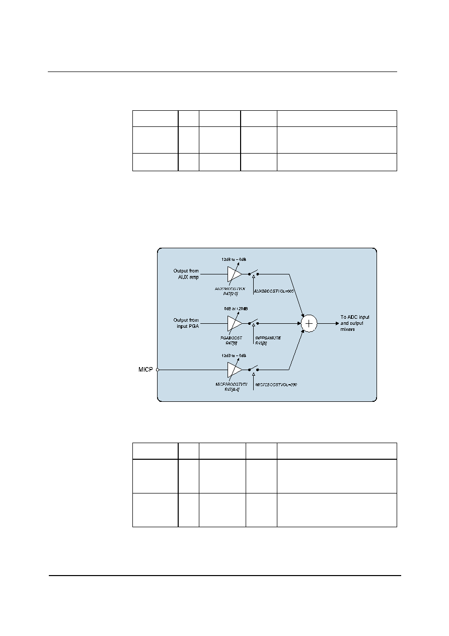
INPUT BOOST
The input BOOST circuit has 3 selectable inputs: the input microphone PGA output, the AUX
amplifier output and the MICP input pin (when not using a differential microphone configuration).
These three inputs can be mixed together and have individual gain boost/adjust as shown in Figure
8.
Figure 8 Input Boost Stage
The input PGA path can have a +20dB boost (PGABOOST=1) a 0dB pass through (PGABOOST=0)
or be completely isolated from the input boost circuit (INPPGAMUTE=1).
REGISTER
ADDRESS
BIT
LABEL
DEFAULT
DESCRIPTION
R45
Input PGA gain
control
6
INPPGAMUTE
0
Mute control for input PGA:
0=Input PGA not muted, normal operation
1=Input PGA muted (and disconnected from
the following input BOOST stage).
R47
Input BOOST
control
8
PGABOOST
1
0 = PGA output has +0dB gain through
input BOOST stage.
1 = PGA output has +20dB gain through
input BOOST stage.
Table 3 Input BOOST Stage Control
The Auxilliary amplifier path to the BOOST stage is controlled by the AUX2BOOSTVOL[2:0] register
bits. When AUX2BOOSTVOL=000 this path is completely disconnected from the BOOST stage.
Settings 001 through to 111 control the gain in 3dB steps from -12dB to +6dB.

WM8974
Product Preview
w
PP Rev 1.1 September 2004
18
The MICP path to the BOOST stage is controlled by the MICP2BOOSTVOL[2:0] register bits.
When MICP2BOOSTVOL=000 this input pin is completely disconnected from the BOOST stage.
Settings 001 through to 111 control the gain in 3dB steps from -12dB to +6dB.
REGISTER
ADDRESS
BIT
LABEL
DEFAULT
DESCRIPTION
2:0
AUX2BOOSTVOL
000
Controls the auxilliary amplifer to the input
boost stage:
000=Path disabled (disconnected)
001=-12dB gain through boost stage
010=-9dB gain through boost stage
...
111=+6dB gain through boost stage
R47
Input BOOST
control
6:4
MICP2BOOSTVOL 000
Controls the MICP pin to the input boost
stage (NB, when using this path set
MICPZIUNPPGA=0):
000=Path disabled (disconnected)
001=-12dB gain through boost stage
010=-9dB gain through boost stage
...
111=+6dB gain through boost stage
Table 4 Input BOOST Stage Control
The BOOST stage is enabled under control of the BOOSTEN register bit.
REGISTER
ADDRESS
BIT
LABEL
DEFAULT
DESCRIPTION
R2
Power
management 2
4
BOOSTEN
0
Input BOOST enable
0 = Boost stage OFF
1 = Boost stage ON
Table 5 Input BOOST Enable Control
MICROPHONE BIASING CIRCUIT
The MICBIAS output provides a low noise reference voltage suitable for biasing electret type
microphones and the associated external resistor biasing network. Refer to the Applications
Information section for recommended external components. The MICBIAS voltage can be altered via
the MBVSEL register bit. When MBVSEL=0, MICBIAS=0.9*AVDD and when MBVSEL=1,
MICBIAS=0.75*AVDD. The output can be enabled or disabled using the MICBEN control bit.
REGISTER
ADDRESS
BIT
LABEL
DEFAULT
DESCRIPTION
R1
Power
management 1
4
MICBEN
0
Microphone Bias Enable
0 = OFF (high impedance output)
1 = ON
REGISTER
ADDRESS
BIT
LABEL
DEFAULT
DESCRIPTION
R44
Input Control
8
MBVSEL
0
Microphone Bias Voltage Control
0 = 0.9 * AVDD
1 = 0.75 * AVDD
The internal MICBIAS circuitry is shown in Figure 9. Note that the maximum source current
capability for MICBIAS is 3mA. The external biasing resistors therefore must be large enough to limit
the MICBIAS current to 3mA.

Product Preview
WM8974
w
PP Rev 1.1 September 2004
19
AGND
MBVSEL=0
MICBIAS
= 1.8 x VMID
= 0.9 X AVDD
VMID
internal
resistor
internal
resistor
MB
MBVSEL=1
MICBIAS
= 1.5 x VMID
= 0.75 X AVDD
Figure 9 Microphone Bias Schematic
ANALOGUE TO DIGITAL CONVERTER (ADC)
The WM8974 uses a multi-bit, oversampled sigma-delta ADC channel. The use of multi-bit feedback
and high oversampling rates reduces the effects of jitter and high frequency noise. The ADC Full
Scale input level is proportional to AVDD. With a 3.3V supply voltage, the full scale level is 1.0V
rms
.
Any voltage greater than full scale may overload the ADC and cause distortion.
ADC DIGITAL FILTERS
The ADC filters perform true 24 bit signal processing to convert the raw multi-bit oversampled data
from the ADC to the correct sampling frequency to be output on the digital audio interface. The
digital filter path is illustrated in Figure 10.
Figure 10 ADC Digital Filter Path
The ADC is enabled by the ADCEN register bit.
REGISTER
ADDRESS
BIT
LABEL
DEFAULT
DESCRIPTION
R2
Power
management 2
0
ADCEN
0
0 = ADC disabled
1 = ADC enabled

WM8974
Product Preview
w
PP Rev 1.1 September 2004
20
The polarity of the output signal can also be changed under software control using the ADCPOL
register bit. The oversampling rate of the ADC can be adjusted using the ADCOSR register bit.
With ADCOSR=0 the oversample rate is 64x which gives lowest power operation and when
ADCOSR=1 the oversample rate is 128x which gives best performance.
REGISTER
ADDRESS
BIT
LABEL
DEFAULT
DESCRIPTION
3
ADCOSR
0
ADC oversample rate select:
0=64x (lower power)
1=128x (best performance)
R14
ADC Control
0
ADCPOL
0
0=normal
1=inverted
SELECTABLE HIGH PASS FILTER
A selectable high pass filter is provided. To disable this filter set HPFEN=0. The filter has two
modes controlled by HPFAPP. In Audio Mode (HPFAPP=0) the filter is first order, with a cut-off
frequency of 3.7Hz. In Application Mode (HPFAPP=1) the filter is second order, with a cut-off
frequency selectable via the HPFCUT register. The cut-off frequencies when HPFAPP=1 are shown
in Table 6.
REGISTER
ADDRESS
BIT
LABEL
DEFAULT
DESCRIPTION
8
HPFEN
1
High Pass Filter Enable
0=disabled
1=enabled
7
HPFAPP
0
Select audio mode or application mode
0=Audio mode (1
st
order, fc = ~3.7Hz)
1=Application mode (2
nd
order, fc =
HPFCUT)
R14
ADC Control
6:4
HPFCUT
000
Application mode cut-off frequency
See Table 6 for details.
FS (KHZ)
SR=101/100
SR=011/010
SR=001/000
HPFCUT
8
11.025
12
16
22.05
24
32
44.1
48
000
82
113
122
82
113
122
82
113
122
001
102
141
153
102
141
153
102
141
153
010
131
180
156
131
180
156
131
180
156
011
163
225
245
163
225
245
163
225
245
100
204
281
306
204
281
306
204
281
306
101
261
360
392
261
360
392
261
360
392
110
327
450
490
327
450
490
327
450
490
111
408
563
612
408
563
612
408
563
612
Table 6 High Pass Filter Cut-off Frequencies (HPFAPP=1)
Note that the High Pass filter values (when HPFAPP=1) work on the basis that the SR register bits
are set correctly for the actual sample rate as shown in Table 6.

Product Preview
WM8974
w
PP Rev 1.1 September 2004
21
PROGRAMMABLE NOTCH FILTER
A programmable notch filter is provided. This filter has a variable centre frequency and bandwidth,
programmable via two coefficients, a0 and a1. a0 and a1 are represented by the register bits
NFA0[13:0] and NFA1[13:0]. Because these coefficient values require four register writes to setup
there is an NFU (Notch Filter Update) flag which should be set only when all four registers are setup.
REGISTER
ADDRESS
BIT
LABEL
DEFAULT
DESCRIPTION
6:0
NFA0[13:7]
0
Notch Filter a0 coefficient, bits [13:7]
7
NFEN
0
Notch filter enable:
0=Disabled
1=Enabled
R27
Notch Filter 1
8
NFU
0
Notch filter update. The notch filter
values used internally only update when
one of the NFU bits is set high.
6:0
NFA0[6:0]
0
Notch Filter a0 coefficient, bits [6:0]
R28
Notch Filter 2
8
NFU]
0
Notch filter update. The notch filter
values used internally only update when
one of the NFU bits is set high.
6:0
NFA1[13:7]
0
Notch Filter a1 coefficient, bits [13:7]
R29
Notch Filter 3
8
NFU
0
Notch filter update. The notch filter
values used internally only update when
one of the NFU bits is set high.
6:0
NFA1[6:0]
0
Notch Filter a1 coefficient, bits [6:0]
R30
Notch Filter 4
8
NFU
0
Notch filter update. The notch filter
values used internally only update when
one of the NFU bits is set high.
Table 7 Notch Filter Function
The coefficients are calculated as follows:
)
2
/
tan(
1
)
2
/
tan(
1
0
b
b
w
w
a
+
-
=
)
cos(
)
1
(
0
0
1
w
a
a
+
-
=
Where:
s
c
f
f
w
/
2
0
=
s
b
b
f
f
w
/
2
=
f
c
= centre frequency in Hz, f
b
= -3dB bandwidth in Hz, f
s
= sample frequency in Hz
The actual register values can be determined from the coefficients as follows:
NFA0 = -a0 x 2
13
NFA1 = -a1 x 2
12

WM8974
Product Preview
w
PP Rev 1.1 September 2004
22
DIGITAL ADC VOLUME CONTROL
The output of the ADCs can be digitally attenuated over a range from ≠127dB to 0dB in 0.5dB steps.
The gain for a given eight-bit code X is given by:
Gain = 0.5 x (x≠255) dB for 1
x 255, MUTE for x = 0
REGISTER
ADDRESS
BIT
LABEL
DEFAULT
DESCRIPTION
R15
ADC Digital
Volume
7:0
ADCVOL
[7:0]
11111111
( 0dB )
Left ADC Digital Volume Control
0000 0000 = Digital Mute
0000 0001 = -127dB
0000 0010 = -126.5dB
... 0.5dB steps up to
1111 1111 = 0dB
INPUT LIMITER / AUTOMATIC LEVEL CONTROL (ALC)
The WM8974 has an automatic pga gain control circuit, which can function as an input peak limiter
or as an automatic level control (ALC).
In input peak limiter mode (ALCMODE bit = 1), a digital peak detector detects when the input signal
goes above a predefined level and will ramp the pga gain down to prevent the signal becoming too
large for the input range of the ADC. When the signal returns to a level below the threshold, the pga
gain is slowly returned to its starting level. The peak limiter cannot increase the pga gain above its
static level.
Figure 11 Input Peak Limiter Operation
In ALC mode (ALCMODE bit = 0) the circuit aims to keep a constant recording volume irrespective
of the input signal level. This is achieved by continuously adjusting the PGA gain so that the signal
level at the ADC input remains constant. A digital peak detector monitors the ADC output and
changes the PGA gain if necessary.

Product Preview
WM8974
w
PP Rev 1.1 September 2004
23
Figure 12 ALC Operation
The ALC/Limiter function is enabled by setting the register bit ALCSEL. When enabled, the
recording volume can be programmed between ≠6dB and ≠28.5dB (relative to ADC full scale) using
the ALCLVL register bits. An upper limit for the PGA gain can be imposed by setting the ALCMAX
control bits and a lower limit for the PGA gain can be imposed by setting the ALCMIN control bits.
ALCHLD, ALCDCY and ALCATK control the hold, decay and attack times, respectively:
Hold time is the time delay between the peak level detected being below target and the PGA gain
beginning to ramp up. It can be programmed in power-of-two (2
n
) steps, e.g. 2.67ms, 5.33ms,
10.67ms etc. up to 43.7s. Alternatively, the hold time can also be set to zero. The hold time is not
active in limiter mode (ALCMODE = 1). The hold time only applies to gain ramp-up, there is no delay
before ramping the gain down when the signal level is above target.
Decay (Gain Ramp-Up) Time is the time that it takes for the PGA gain to ramp up and is given as a
time per gain step, time per 6dB change and time to ramp up over 90% of it's range. The decay
time can be programmed in power-of-two (2
n
) steps, from 3.3ms/6dB, 6.6ms/6dB, 13.1ms/6dB, etc.
to 3.36s/6dB.
Attack (Gain Ramp-Down) Time is the time that it takes for the PGA gain to ramp down and is given
as a time per gain step, time per 6dB change and time to ramp down over 90% of it's range. The
attack time can be programmed in power-of-two (2
n
) steps, from 832us/6dB, 1.66ms/6dB,
3.328us/6dB, etc. to 852ms/6dB.
NB, In peak limiter mode the gain control circuit runs approximately 4x faster to allow reduction of
fast peaks. Attack and Decay times for peak limiter mode are given below.
The hold, decay and attack times given in Table 8 are constant across sample rates so long as the
SR bits are set correctly. E.g. when sampling at 48kHz the sample rates stated in Table 8 will only
be correct if the SR bits are set to 000 (48kHz). If the actual sample rate was only 44.1kHz then the
hold, decay and attack times would be scaled down by 44.1/48.

WM8974
Product Preview
w
PP Rev 1.1 September 2004
24
REGISTER
ADDRESS
BIT
LABEL
DEFAULT
DESCRIPTION
8
ALCSEL
0
ALC function select
0=ALC disabled
1=ALC enabled
5:3
ALCMAXGAIN
[2:0]
111
(+35.25dB)
Set Maximum Gain of PGA
111=+35.25dB
110=+29.25dB
101=+23.25dB
100=+17.25dB
011=+11.25dB
010=+5.25dB
001=-0.75dB
000=-6.75dB
R32
ALC Control 1
2:0
ALCMINGAIN
[2:0]
000 (-12dB)
Set minimum gain of PGA
000=-12dB
001=-6dB
010=0dB
011=+6dB
100=+12dB
101=+18dB
110=+24dB
111=+30dB
7:4
ALCHLD
[3:0]
0000
(0ms)
ALC hold time before gain is increased.
0000 = 0ms
0001 = 2.67ms
0010 = 5.33ms
... (time doubles with every step)
1111 = 43.691s
3:0
ALCLVL
[3:0]
1011
(-12dB)
ALC target ≠ sets signal level at ADC
input
0000 = -28.5dB FS
0001 = -27.0dB FS
... (1.5dB steps)
1110 = -7.5dB FS
1111 = -6dB FS
R33
ALC Control 2
8
ALCZC
0 (zero cross
off)
ALC uses zero cross detection circuit.

Product Preview
WM8974
w
PP Rev 1.1 September 2004
25
8
ALCMODE
0
Determines the ALC mode of operation:
0=ALC mode
1=Limiter mode.
Decay (gain ramp-up) time
(ALCMODE =0)
Per step Per 6dB
90% of
range
0000
410us
3.3ms
24ms
0001
820us
6.6ms
48ms
0010
1.64ms
13.1ms
192ms
... (time doubles with every step)
0011
(13ms/6dB)
1010 or
higher
420ms
3.36s
24.576s
Decay (gain ramp-up) time
(ALCMODE =1)
Per step Per 6dB
90% of
range
0000
90.8us
726.4us
5.26ms
0001
181.6us
1.453ms 10.53ms
0010
363.2us
2.905ms 21.06ms
... (time doubles with every step)
7:4
ALCDCY
[3:0]
0011
(2.9ms/6dB)
1010
93ms
744ms
5.39s
ALC attack (gain ramp-down) time
(ALCMODE = 0)
Per step Per 6dB
90% of
range
0000
104us
832us
6ms
0001
208us
1.664ms 12ms
0010
416us
3.328ms 24.1ms
... (time doubles with every step)
0010
(832us/6dB)
1010 or
higher
106ms
852ms
6.18s
ALC attack (gain ramp-down) time
(ALCMODE = 1)
Per step Per 6dB
90% of
range
0000
22.7us
182.4us
1.31ms
0001
45.4us
363.2us
2.62ms
0010
90.8us
726.4us
5.26ms
... (time doubles with every step)
R34
ALC Control 3
3:0
ALCATK
[3:0]
0010
(182us/6dB)
1010
23.2ms
186ms
1.348s
Table 8 ALC Control Registers
WM8974
Product Preview
w
PP Rev 1.1 September 2004
26
ALC CLIP PROTECTION
To prevent clipping when a large signal occurs just after a period of quiet, the ALC circuit includes a
clip protection function. If the ADC input signal exceeds 87.5% of full scale (≠1.16dB), the PGA gain
is ramped down at the maximum attack rate (as when ALCATK = 0000), until the signal level falls
below 87.5% of full scale. This function is automatically enabled whenever the ALC is enabled.
Note:
If ATK = 0000, then the clip protection circuit makes no difference to the operation of the ALC. It is
designed to prevent clipping when long attack times are used.
NOISE GATE
When the signal is very quiet and consists mainly of noise, the ALC function may cause "noise
pumping", i.e. loud hissing noise during silence periods. The WM8974 has a noise gate function that
prevents noise pumping by comparing the signal level at the input pins against a noise gate
threshold, NGTH. The noise gate cuts in when:
Signal level at ADC [dB] < NGTH [dB] + PGA gain [dB] + Mic Boost gain [dB]
This is equivalent to:
Signal level at input pin [dB] < NGTH [dB]
The PGA gain is then held constant (preventing it from ramping up as it normally would when the
signal is quiet).
The table below summarises the noise gate control register. The NGTH control bits set the noise
gate threshold with respect to the ADC full-scale range. The threshold is adjusted in 6dB steps.
Levels at the extremes of the range may cause inappropriate operation, so care should be taken with
set≠up of the function. Note that the noise gate only works in conjunction with the ALC function.
REGISTER
ADDRESS
BIT
LABEL
DEFAULT
DESCRIPTION
2:0
NGTH
000
Noise gate threshold:
000=-39dB
001=-45dB
010=-51db
... (6dB steps)
111=-81dB
R35
ALC Noise Gate
Control
3
NGATEN
0
Noise gate function enable
1 = enable
0 = disable
Table 9 ALC Noise Gate Control
OUTPUT SIGNAL PATH
The WM8974 output signal paths consist of digital application filters, up-sampling filters, a Hi-Fi
DAC, analogue mixers, speaker and mono output drivers. The digital filters and DAC are enabled by
bit DACEN. The mixers and output drivers can be separately enabled by individual control bits (see
Analogue Outputs). Thus it is possible to utilise the analogue mixing and amplification provided by
the WM8974, irrespective of whether the DACs are running or not.
The WM8974 DAC receives digital input data on the DACDAT pin. The digital filter block processes
the data to provide the following functions:
ß
Digital volume control
ß
Graphic equaliser
ß
A digital peak limiter.
ß
Sigma-Delta Modulation
The high performance sigma-delta audio DAC converts the digital data into an analogue signal.

Product Preview
WM8974
w
PP Rev 1.1 September 2004
27
Figure 13 DAC Digital Filter Path
The analogue output from the DAC can then be mixed with the AUX analogue input and the ADC
analogue input. The mix is fed to the output drivers, SPKROUTP/N, and MONOOUT.
MONOOUT: can drive a 16
or 32 headphone or line output or can be a buffered version of VMID
(When MONOMUTE=1).
SPKROUTP/N: can drive a 16
or 32 stereo headphone or stereo line output, or an 8 BTL mono
speaker.
DIGITAL HI-FI DAC VOLUME CONTROL
The signal volume from each Hi-Fi DAC can be controlled digitally. The gain and attenuation range
is ≠127dB to 0dB in 0.5dB steps. The level of attenuation for an eight-bit code X is given by:
0.5
◊ (X-255) dB for 1 X 255;
MUTE for X = 0
REGISTER
ADDRESS
BIT
LABEL
DEFAULT
DESCRIPTION
R11
DAC Digital
Volume
7:0
DACVOL
[7:0]
11111111
( 0dB )
Left DAC Digital Volume Control
0000 0000 = Digital Mute
0000 0001 = -127dB
0000 0010 = -126.5dB
... 0.5dB steps up to
1111 1111 = 0dB
HI-FI DIGITAL TO ANALOGUE CONVERTER (DAC)
After passing through the graphic equaliser filters, digital `de-emphasis' can be applied to the audio
data if necessary (e.g. when the data comes from a CD with pre-emphasis used in the recording).
De-emphasis filtering is available for sample rates of 48kHz, 44.1kHz and 32kHz.
The DAC is enabled by the DACEN register bit..
REGISTER
ADDRESS
BIT
LABEL
DEFAULT
DESCRIPTION
R3
Power
Management 3
0
DACEN
0
DAC enable
0 = DAC disabled
1 = DAC enabled
The WM8974 also has a Soft Mute function, which gradually attenuates the volume of the digital
signal to zero. When removed, the gain will ramp back up to the digital gain setting. This function is
enabled by default. To play back an audio signal, it must first be disabled by setting the DACMU bit
to zero.

WM8974
Product Preview
w
PP Rev 1.1 September 2004
28
REGISTER
ADDRESS
BIT
LABEL
DEFAULT
DESCRIPTION
6
DACMU
1
DAC Softmute:
0 = Unmuted
1 = Muted
5:4
DEEMP
[1:0]
00
De-emphasis Control:
00 = No De-emphasis
01 = 32kHz sample rate
10 = 44.1kHz sample rate
11 = 48kHz sample rate
3
DACOSR
0
DAC oversampling rate:
0=64x (lowest power)
1=128x (best performance)
2
AMUTE
0
Automute enable
0 = Amute disabled
1 = Amute enabled
R10
DAC Control
0
DACPOL
0
DAC output polarity:
0 = non-inverted
1 = inverted (180 degrees phase shift)
Table 10 DAC Control Register
The digital audio data is converted to oversampled bit streams in the on-chip, true 24-bit digital
interpolation filters. The bitstream data enters a multi-bit, sigma-delta DAC, which converts it to a
high quality analogue audio signal. The multi-bit DAC architecture reduces high frequency noise and
sensitivity to clock jitter.
The DAC output defaults to non-inverted. Setting DACPOL will invert the DAC output phase on both
left and right channels.
AUTOMUTE
The DAC has an automute function which applied an analogue mute when 1024 consecutive zeros
are detected. The mute is release as soon as a non-zero sample is detected. Automute can be
disabled using the AMUTE control bit.
DAC OUTPUT LIMITER
The WM8974 has a digital output limiter function. The operation of this is shown in Figure 14. In
this diagram the upper graph shows the envelope of the input/output signals and the lower graph
shows the gain characteristic.

Product Preview
WM8974
w
PP Rev 1.1 September 2004
29
Figure 14 DAC Digital Limiter Operation
The limiter has a programmable upper threshold which is close to 0dB. Referring to Figure 14, in
normal operation (LIMBOOST=000 => limit only) signals below this threshold are unaffected by the
limiter. Signals above the upper threshold are attenuated at a specific attack rate (set by the
LIMATK register bits) until the signal falls below the threshold. The limiter also has a lower threshold
1dB below the upper threshold. When the signal falls below the lower threshold the signal is
amplified at a specific decay rate (controlled by LIMDCY register bits) until a gain of 0dB is reached.
Both threshold levels are controlled by the LIMLVL register bits. The upper threshold is 0.5dB above
the value programmed by LIMLVL and the lower threshold is 0.5dB below the LIMLVL value.
VOLUME BOOST
The limiter has programmable upper gain which boosts signals below the threshold to compress the
dynamic range of the signal and increase its perceived loudness. This operates as an ALC function
with limited boost capability. The volume boost is from 0dB to +12dB in 1dB steps, controlled by the
LIMBOOST register bits.
The output limiter volume boost can also be used as a stand alone digital gain boost when the limiter
is disabled.

WM8974
Product Preview
w
PP Rev 1.1 September 2004
30
REGISTER
ADDRESS
BIT
LABEL
DEFAULT
DESCRIPTION
3:0
LIMATK
0010
Limiter Attack time (per 6dB gain change)
for 44.1kHz sampling. Note that these will
scale with sample rate.
0000=94us
0001=188s
0010=375us
0011=750us
0100=1.5ms
0101=3ms
0110=6ms
0111=12ms
1000=24ms
1001=48ms
1010=96ms
1011 to 1111=192ms
7:4
LIMDCY
0011
Limiter Decay time (per 6dB gain change)
for 44.1kHz sampling. Note that these will
scale with sample rate:
0000=750us
0001=1.5ms
0010=3ms
0011=6ms
0100=12ms
0101=24ms
0110=48ms
0111=96ms
1000=192ms
1001=384ms
1010=768ms
1011 to 1111=1.536s
R24
DAC digital
limiter control 1
8
LIMEN
0
Enable the DAC digital limiter:
0=disabled
1=enabled
3:0
LIMBOOST
0000
Limiter volume boost (can be used as a
stand alone volume boost when
LIMEN=0):
0000=0dB
0001=+1dB
0010=+2dB
... (1dB steps)
1011=+11dB
1100=+12dB
1101 to 1111=reserved
R25
DAC digital
limiter control 2
6:4
LIMLVL
000
Programmable signal threshold level
(determines level at which the limiter
starts to operate)
000=-1dB
001=-2dB
010=-3dB
011=-4dB
100=-5dB
101 to 111=-6dB
Table 11 DAC Digital Limiter Control

Product Preview
WM8974
w
PP Rev 1.1 September 2004
31
GRAPHIC EQUALISER
A 5-band graphic EQ is provided, which can be applied to the ADC or DAC path under control of the
EQMODE register bit.
REGISTER
ADDRESS
BIT
LABEL
DEFAULT
DESCRIPTION
R18
EQ Control 1
8
EQMODE
1
0 = Equaliser applied to ADC path
1 = Equaliser applied to DAC path
Table 12 EQ DAC or ADC Path Select
The equaliser consists of low and high frequency shelving filters (Band 1 and 5) and three peak
filters for the centre bands. Each has adjustable cut-off or centre frequency, and selectable boost
(+/- 12dB in 1dB steps). The peak filters have selectable bandwidth.
REGISTER
ADDRESS
BIT
LABEL
DEFAULT
DESCRIPTION
4:0
EQ1G
01100
(0dB)
Band 1 Gain Control. See Table 18 for
details.
R18
EQ Band 1
Control
6:5
EQ1C
01
Band 1 Cut-off Frequency:
00=80Hz
01=105Hz
10=135Hz
11=175Hz
Table 13 EQ Band 1 Control
REGISTER
ADDRESS
BIT
LABEL
DEFAULT
DESCRIPTION
4:0
EQ2G
01100
(0dB)
Band 2 Gain Control. See Table 18 for
details.
6:5
EQ2C
01
Band 2 Centre Frequency:
00=230Hz
01=300Hz
10=385Hz
11=500Hz
R19
EQ Band 2
Control
8
EQ2BW
0
Band 2 Bandwidth Control
0=narrow bandwidth
1=wide bandwidth
Table 14 EQ Band 2 Control
REGISTER
ADDRESS
BIT
LABEL
DEFAULT
DESCRIPTION
4:0
EQ3G
01100
(0dB)
Band 3 Gain Control. See Table 18 for
details.
6:5
EQ3C
01
Band 3 Centre Frequency:
00=650Hz
01=850Hz
10=1.1kHz
11=1.4kHz
R20
EQ Band 3
Control
8
EQ3BW
0
Band 3 Bandwidth Control
0=narrow bandwidth
1=wide bandwidth
Table 15 EQ Band 3 Control

WM8974
Product Preview
w
PP Rev 1.1 September 2004
32
REGISTER
ADDRESS
BIT
LABEL
DEFAULT
DESCRIPTION
4:0
EQ4G
01100
(0dB)
Band 4 Gain Control. See Table 18 for
details
6:5
EQ4C
01
Band 4 Centre Frequency:
00=1.8kHz
01=2.4kHz
10=3.2kHz
11=4.1kHz
R21
EQ Band 4
Control
8
EQ4BW
0
Band 4 Bandwidth Control
0=narrow bandwidth
1=wide bandwidth
Table 16 EQ Band 4 Control
REGISTER
ADDRESS
BIT
LABEL
DEFAULT
DESCRIPTION
4:0
EQ5G
01100
(0dB)
Band 5 Gain Control. See Table 18 for
details.
R22
EQ Band 5
Gain Control
6:5
EQ5C
01
Band 5 Cut-off Frequency:
00=5.3kHz
01=6.9kHz
10=9kHz
11=11.7kHz
Table 17 EQ Band 5 Control
GAIN REGISTER
GAIN
00000
+12dB
00001
+11dB
00010
+10dB
.... (1dB steps)
01100
0dB
01101
-1dB
11000 to 11111
-12dB
Table 18 Gain Register Table

Product Preview
WM8974
w
PP Rev 1.1 September 2004
33
ANALOGUE OUTPUTS
The WM8974 has a single MONO output and two outputs SPKOUTP and SPOUTN for driving a
mono BTL speaker. These analogue output stages are supplied from SPKRVDD and are capable of
driving up to 1.5V rms signals (equivalent to 3V rms into a bridge tied speaker) as shown in Figure
15.
Figure 15 Speaker and Mono Analogue Outputs
The Mono and speaker outputs have output driving stages which can be controlled by the register
bits MONOBOOST and SPKBOOST respectively. Each output stage has a selectable gain boost of
1.5x. When this boost is enabled the output DC level is also level shifted (from AVDD/2 to
1.5xAVDD/2) to prevent the signal from clipping. A dedicated amplifier, as shown in Figure 15, is
used to perform the DC level shift operation. This buffer must be enabled using the BUFDCOPEN
register bit for this operating mode. It should also be noted that if SPKRVDD is not equal to or
greater than 1.5xAVDD this boost mode may result in signals clipping. Table 20 summarises the
effect of the SPKRBOOST/MONOBOOST control bits.

WM8974
Product Preview
w
PP Rev 1.1 September 2004
34
REGISTER
ADDRESS
BIT
LABEL
DEFAULT
DESCRIPTION
2
SPKBOOST
0
Speaker output boost stage control (see
Table 20 for details)
0=No boost (outputs are inverting buffers)
1 = 1.5x gain boost
R49
Output control
3
MONOBOOST
0
Mono output boost stage control (see
Table 20 for details)
0=No boost (output is inverting buffer)
1=1.5x gain boost
R1
Power
management 1
8
BUFDCOPEN
0
Dedicated buffer for DC level shifting
output stages when in 1.5x gain boost
configuration.
0=Buffer disabled
1=Buffer enabled (required for 1.5x gain
boost)
Table 19 Output Boost Control
SPKBOOST/
MONOBOOST
OUTPUT
STAGE GAIN
OUTPUT DC
LEVEL
OUTPUT STAGE
CONFIGURATION
0
1x
AVDD/2
Inverting
1
1.5x
1.5xAVDD/2
Non-inverting
Table 20 Output Boost Stage Details
SPKROUTP/SPKROUTN OUTPUTS
The SPKROUT pins can drive a single bridge tied 8 speaker or two headphone loads of 16
or
32
or a line output (see Headphone Output and Line Output sections, respectively). The signal to
be output on SKPKOUT comes from the Speaker Mixer circuit and can be any combination of the
DAC output, the Bypass path (output of the boost stage) and the AUX input. The SPKROUTP/N
volume is controlled by the SPKRVOL register bits. Note that gains over 0dB may cause clipping if
the signal is large. The SPKMUTE register bit causes the speaker outputs to be muted (the output
DC level is driven out). The output pins remains at the same DC level (VMIDOP), so that no click
noise is produced when muting or un-muting.
The SPKROUTN pin always drives out an inverted version of the SPKROUTP signal.
REGISTER
ADDRESS
BIT
LABEL
DEFAULT
DESCRIPTION
0
DAC2SPK
1
Output of DAC to speaker mixer input
0 = not selected
1 = selected
1
BYP2SPK
0
Bypass path (output of input boost
stage) to speaker mixer input
0 = not selected
1 = selected
R50
Speaker mixer
control
5
AUX2SPK
0
Output of auxiliary amplifier to speaker
mixer input
0 = not selected
1 = selected
Table 21 Speaker Mixer Control

Product Preview
WM8974
w
PP Rev 1.1 September 2004
35
REGISTER
ADDRESS
BIT
LABEL
DEFAULT
DESCRIPTION
7
SPKZC
0
Speaker Volume control zero cross
enable:
1 = Change gain on zero cross only
0 = Change gain immediately
6
SPKMUTE
0
Speaker output mute enable
0=Speaker output enabled
1=Speaker output muted (VMIDOP)
R54
Speaker
volume control
5:0
SPKRVOL
[5:0]
111001
(0dB)
Speaker Volume Adjust
111111 = +6dB
111110 = +5dB
... (1.0 dB steps)
111001=0dB
...
000000=-57dB
Table 22 SPKROUT Volume Control
ZERO CROSS TIMEOUT
A zero-cross timeout function is also provided so that if zero cross is enabled on the input or output
PGAs the gain will automatically update after a timeout period if a zero cross has not occurred. This
is enabled by setting SLOWCLKEN. The timeout period is dependent on the clock input to the digital
and is equal to 2
21
* input clock period.
REGISTER
ADDRESS
BIT
LABEL
DEFAULT
DESCRIPTION
R7
Additional
control
0
SLOWCLKEN
0
Slow clock enable. Used for both the jack
insert detect debounce circuit and the
zero cross timeout.
0 = slow clock disabled
1 = slow clock enabled
Table 23 Timeout Clock Enable Control
MONO MIXER AND OUTPUT
The MONOOUT pin can drive a 16
or 32 headphone or a line output or be used as a DC
reference for a headphone output (see Headphone Output section). It can be selected to drive out
any combination of DAC, Bypass (output of input BOOST stage) and AUX. This output is enabled
by setting bit MONOEN.

WM8974
Product Preview
w
PP Rev 1.1 September 2004
36
REGISTER
ADDRESS
BIT
LABEL
DEFAULT
DESCRIPTION
0
DAC2MONO
0
Output of DAC to mono mixer input
0 = not selected
1 = selected
1
BYP2MONO
0
Bypass path (output of input boost
stage) to mono mixer input
0 = non selected
1 = selected
2
AUX2MONO
0
Output of Auxillary amplifier to mono
mixer input:
0 = not selected
1 = selected
R56
Mono mixer
control
6
MONOMUTE
0
0=No mute
1=Output muted. During mute the
mono output will output VMID which can
be used as a DC reference for a
headphone out.
Table 24 Mono Mixer Control
ENABLING THE OUTPUTS
Each analogue output of the WM8974 can be separately enabled or disabled. The analogue mixer
associated with each output has a separate enable. All outputs are disabled by default. To save
power, unused parts of the WM8974 should remain disabled.
Outputs can be enabled at any time, but it is not recommended to do so when BUFIO is disabled
(BUFIOEN=0), as this may cause pop noise (see "Power Management" and "Applications
Information" sections).
REGISTER
ADDRESS
BIT
LABEL
DEFAULT
DESCRIPTION
2
BUFIOEN
0
Unused input/output tie off buffer enable
R1
Power
management 1
8
BUFDCOPEN 0
Output stage 1.5xAVDD/2 driver enable
2
SPKMIXEN
0
Speaker Mixer enable
3
MONOMIXEN 0
Mono mixer enable
5
SPKPEN
0
SPKROUTP enable
6
SPKNEN
0
SPKROUTN enable
R3
Power
management 3
7
MONOEN
0
MONOOUT enable
Note: All "Enable" bits are 1 = ON, 0 = OFF
Table 25 Output Stages Power Management Control
UNUSED ANALOGUE INPUTS/OUTPUTS
Whenever an analogue input/output is disabled, it remains connected to a voltage source (either
AVDD/2 or 1.5xAVDD/2 as appropriate) through a resistor. This helps to prevent pop noise when the
output is re-enabled. The resistance between the voltage buffer and the output pins can be
controlled using the VROI contol bit. The default impedance is low, so that any capacitors on the
outputs can charge up quickly at start-up. If a high impedance is desired for disabled outputs, VROI
can then be set to 1, increasing the resistance to about 30k
.

Product Preview
WM8974
w
PP Rev 1.1 September 2004
37
REGISTER
ADDRESS
BIT
LABEL
DEFAULT
DESCRIPTION
R49
0
VROI
0
VREF (AVDD/2 or 1.5xAVDD/2) to
analogue output resistance
0: approx 1k
1: approx 30 k
Table 26 Disabled Outputs to VREF Resistance
A dedicated buffer is available for tieing off unused analogue I/O pins as shown in Figure 16. This
buffer can be enabled using the BUFIOEN register bit.
If the SPKBOOST or MONOBOOST bits are set then the relevant outputs will be tied to the output of
the DC level shift buffer at 1.5xAVDD/2 when disabled.
Table 27 summarises the tie-off options for the speaker and mono output pins.
Figure 16 Unused Input/Output Pin Tie-off Buffers
MONOEN/
SPKN/PEN
MONOBOOST/
SPKRBOOST
VROI
OUTPUT CONFIGURATION
0
0
0
1k tieoff to AVDD/2
0
0
1
30k tieoff to AVDD/2
0
1
0
1k tieoff to 1.5xAVDD/2
0
1
1
30k tieoff to 1.5xAVDD/2
1
0
X
Output enabled (DC level=AVDD/2)
1
1
X
Output enabled (DC level=1.5xAVDD/2)
Table 27 Unused Output Pin Tie-off Options

WM8974
Product Preview
w
PP Rev 1.1 September 2004
38
OUTPUT SWITCH
When the device is configured with a 2-wire interface the CSB/GPIO pin can be used as a switch
control input to automatically disable the speaker outputs and enable the mono output. For example
when a line is plugged into a jack socket. In this mode, enabled by setting GPIOSEL=001, pin
CSB/GPIO switches between mono and speaker outputs (e.g. when pin 12 is connected to a
mechanical switch in the headphone socket to detect plug-in). The GPIOPOL bit reverses the
polarity of the CSB/GPIO input pin.
Note that the speaker outputs and the mono output must be enabled for this function to work (see
Table 28). The CSB/GPIO pin has an internal de-bounce circuit when in this mode in order to
prevent the output enables from toggling multiple times due to input glitches. This debounce circuit
is clocked from a slow clock with period 2
21
x MCLK, enabled using the SLOWCLKEN register bit.
GPIOPOL
CSB/GPIO
SPKNEN/
SPKPEN
MONOEN
SPEAKER
ENABLED
MONO
OUTPUT
ENABLED
0
0
X
0
No
No
0
0
X
1
No
Yes
0
1
0
X
No
No
0
1
1
X
Yes
No
1
0
X
0
No
No
1
0
X
1
No
Yes
1
1
0
X
No
No
1
1
1
X
Yes
No
Table 28 Output Switch Operation (GPIOSEL=001)
THERMAL SHUTDOWN
The speaker outputs can drive very large currents. To protect the WM8974 from overheating a
thermal shutdown circuit is included. If the device temperature reaches approximately 125
0
C and the
thermal shutdown circuit is enabled (TSDEN=1) then the speaker amplifiers will be disabled if
TSDEN is set. The thermal shutdown may also be configured to generate an interrupt. See the GPIO
and Interrupt Controller section for details.
REGISTER
ADDRESS
BIT
LABEL
DEFAULT
DESCRIPTION
R49
Output control
1
TSDEN
1
Thermal Shutdown Enable
0 : thermal shutdown disabled
1 : thermal shutdown enabled
Table 29 Thermal Shutdown
SPEAKER OUTPUT
SPKROUTP/N can differentially drive a mono 8
Bridge Tied Load (BTL) speaker as shown below.
Figure 17 Speaker Output Connection

Product Preview
WM8974
w
PP Rev 1.1 September 2004
39
HEADPHONE OUTPUT
The speaker outputs can drive a 16
or 32 headphone load, either through DC blocking
capacitors, or DC coupled without any capacitor.
Headphone Output using DC Blocking Capacitors:
DC Coupled Headphone Output:
Figure 18 Recommended Headphone Output Configurations
When DC blocking capacitors are used, then their capacitance and the load resistance together
determine the lower cut-off frequency, f
c
. Increasing the capacitance lowers f
c
, improving the bass
response. Smaller capacitance values will diminish the bass response. Assuming a 16
load and
C1, C2 = 220
µF:
f
c
= 1 / 2
R
L
C
1
= 1 / (2
x 16 x 220µF) = 45 Hz
In the DC coupled configuration, the headphone "ground" is connected to the MONOOUT pin. The
MONOOUT pin can be configured as a DC output driver by setting the MONOMUTE register bit.
The DC voltage on MONOOUT in this configuration is equal to the DC offset on the SPROUTP and
SPKOUTN pins therefore no DC blocking capacitors are required. This saves space and material
cost in portable applications.
It is recommended to connect the DC coupled outputs only to headphones, and not to the line input
of another device. Although the built-in short circuit protection will prevent any damage to the
headphone outputs, such a connection may be noisy, and may not function properly if the other
device is grounded.
MONO OUTPUT
The mono output, can be used as a line output, a headphone output or as a puedo ground for cap-
less driving of loads by SPKROUT. Recommended external components are shown below.
Figure 19 Recommended Circuit for Line Output
The DC blocking capacitors and the load resistance together determine the lower cut-off frequency,
f
c
. Assuming a 10 k
load and C1 = 1µF:
f
c
= 1 / 2
(R
L
+R
1
) C
1
= 1 / (2
x 10.1k x 1µF) = 16 Hz
Increasing the capacitance lowers f
c
, improving the bass response. Smaller values of C1 will
diminish the bass response. The function of R1 is to protect the line outputs from damage when
used improperly.

WM8974
Product Preview
w
PP Rev 1.1 September 2004
40
DIGITAL AUDIO INTERFACES
The audio interface has four pins:
∑
ADCDAT: ADC data output
∑
DACDAT: DAC data input
∑
FRAME: Data alignment clock
∑
BCLK: Bit clock, for synchronisation
The clock signals BCLK, and FRAME can be outputs when the WM8974 operates as a master, or
inputs when it is a slave (see Master and Slave Mode Operation, below).
Five different audio data formats are supported:
∑
Left justified
∑
Right justified
∑
I
2
S
∑
DSP mode early
∑
DSP mode late
All of these modes are MSB first. They are described in Audio Data Formats, below. Refer to the
Electrical Characteristic section for timing information.
MASTER AND SLAVE MODE OPERATION
The WM8974 audio interface may be configured as either master or slave. As a master interface
device the WM8974 generates BCLK and FRAME and thus controls sequencing of the data transfer
on ADCDAT and DACDAT. To set the device to master mode register bit MS should be set high. In
slave mode (MS=0), the WM8974 responds with data to clocks it receives over the digital audio
interfaces.
AUDIO DATA FORMATS
In Left Justified mode, the MSB is available on the first rising edge of BCLK following an FRAME
transition. The other bits up to the LSB are then transmitted in order. Depending on word length,
BCLK frequency and sample rate, there may be unused BCLK cycles before each FRAME transition.
Figure 20 Left Justified Audio Interface (assuming n-bit word length)
In Right Justified mode, the LSB is available on the last rising edge of BCLK before a FRAME
transition. All other bits are transmitted before (MSB first). Depending on word length, BCLK
frequency and sample rate, there may be unused BCLK cycles after each FRAME transition.

Product Preview
WM8974
w
PP Rev 1.1 September 2004
41
Figure 21 Right Justified Audio Interface (assuming n-bit word length)
In I
2
S mode, the MSB is available on the second rising edge of BCLK following a FRAME transition.
The other bits up to the LSB are then transmitted in order. Depending on word length, BCLK
frequency and sample rate, there may be unused BCLK cycles between the LSB of one sample and
the MSB of the next.
Figure 22 I
2
S Audio Interface (assuming n-bit word length)
In DSP/PCM mode, the left channel MSB is available on either the 1
st
(mode B) or 2
nd
(mode A)
rising edge of BCLK (selectable by FRAMEP) following a rising edge of FRAME. Depending on word
length, BCLK frequency and sample rate, there may be unused BCLK cycles between the LSB of the
right channel data and the next sample.

WM8974
Product Preview
w
PP Rev 1.1 September 2004
42
Figure 23 DSP/PCM Mode Audio Interface (mode A, FRAMEP=0)
Figure 24 DSP/PCM Mode Audio Interface (mode B, FRAMEP=1)
When using ADCLRSWAP = 1 or DACLRSWAP = 1 in DSP/PCM mode, the data will appear in the
Right Phase of the FRAME, which will be 16/20/24/32 bits after the FRAME pulse.

Product Preview
WM8974
w
PP Rev 1.1 September 2004
43
REGISTER
ADDRESS
BIT
LABEL
DEFAULT
DESCRIPTION
1
ADCLRSWAP
0
Controls whether ADC data appears in
`right' or `left' phases of FRAME clock:
0=ADC data appear in `left' phase of
FRAME
1=ADC data appears in `right' phase of
FRAME
2
DACLRSWAP
0
Controls whether DAC data appears in
`right' or `left' phases of FRAME clock:
0=DAC data appear in `left' phase of
FRAME
1=DAC data appears in `right' phase of
FRAME
4:3
FMT
10
Audio interface Data Format Select:
00=Right Justified
01=Left Justified
10=I
2
S format
11= DSP/PCM mode
6:5
WL
10
Word length
00=16 bits
01=20 bits
10=24 bits
11=32 bits (see note)
Frame clock polarity
0=normal
1=inverted
7
FRAMEP
0
DSP Mode ≠ mode A/B select
1 = MSB is available on 1st BCLK rising
edge after FRAME rising edge (mode B)
0 = MSB is available on 2nd BCLK rising
edge after FRAME rising edge (mode A)
R4
Audio interface
control
8
BCP
0
BCLK polarity
0=normal
1=inverted
Table 30 Audio Interface Control
Audio Interface Control
The register bits controlling audio format, word length and master / slave mode are summarised
below. Each audio interface can be controlled individually.
Register bit MS selects audio interface operation in master or slave mode. In Master mode BCLK,
and FRAME are outputs. The frequency of BCLK and FRAME in master mode are controlled with
BCLKDIV. These are divided down versions of master clock. This may result in short BCLK pulses
at the end of a frame if there is a non-integer ratio of BCLKs to FRAME clocks.

WM8974
Product Preview
w
PP Rev 1.1 September 2004
44
REGISTER
ADDRESS
BIT
LABEL
DEFAULT
DESCRIPTION
0
MS
0
Sets the chip to be master over FRAME
and BCLK
0=BCLK and FRAME clock are inputs
1=BCLK and FRAME clock are outputs
generated by the WM8974 (MASTER)
4:2
BCLKDIV
000
Configures the BCLK and FRAME output
frequency, for use when the chip is
master over BCLK.
000=divide by 1 (BCLK=MCLK)
001=divide by 2 (BCLK=MCLK/2)
010=divide by 4
011=divide by 8
100=divide by 16
101=divide by 32
110=reserved
111=reserved
7:5
MCLKDIV
010
Sets the scaling for either the MCLK or
PLL clock output (under control of
CLKSEL)
000=divide by 1
001=divide by 1.5
010=divide by 2
011=divide by 3
100=divide by 4
101=divide by 6
110=divide by 8
111=divide by 12
R6
Clock
generation
control
8
CLKSEL
1
Controls the source of the clock for all
internal operation:
0=MCLK
1=PLL output
Table 31 Clock Control
LOOPBACK
Setting the LOOPBACK register bit enables digital loopback. When this bit is set the output data
from the ADC audio interface is fed directly into the DAC data input.
COMPANDING
The WM8974 supports A-law and
µ-law companding on both transmit (ADC) and receive (DAC)
sides. Companding can be enabled on the DAC or ADC audio interfaces by writing the appropriate
value to the DAC_COMP or ADC_COMP register bits respectively.

Product Preview
WM8974
w
PP Rev 1.1 September 2004
45
REGISTER
ADDRESS
BIT
LABEL
DEFAULT
DESCRIPTION
0
LOOPBACK
0
Digital loopback function
0=No loopback
1=Loopback enabled, ADC data output is
ded directly into DAC data input.
2:1
ADC_COMP
0
ADC companding
00=off
01=reserved
10=µ-law
11=A-law
R5
Companding
control
4:3
DAC_COMP
0
DAC companding
00=off
01=reserved
10=µ-law
11=A-law
Table 32 Companding Control
Companding involves using a piecewise linear approximation of the following equations (as set out
by ITU-T G.711 standard) for data compression:
µ-law (where µ=255 for the U.S. and Japan):
F(x) = ln( 1 +
µ|x|) / ln( 1 + µ) -1 x 1
A-law (where A=87.6 for Europe):
F(x) = A|x| / ( 1 + lnA)
} for x 1/A
F(x) = ( 1 + lnA|x|) / (1 + lnA)
} for 1/A x 1
The companded data is also inverted as recommended by the G.711 standard (all 8 bits are inverted
for
µ-law, all even data bits are inverted for A-law). The data will be transmitted as the first 8 MSB's
of data.
Companding converts 13 bits (
µ-law) or 12 bits (A-law) to 8 bits using non-linear quantization. The
input data range is separated into 8 levels, allowing low amplitude signals better precision than that
of high amplitude signals. This is to exploit the operation of the human auditory system, where
louder sounds do not require as much resolution as quieter sounds. The companded signal is an 8-
bit word containing sign (1-bit), exponent (3-bits) and mantissa (4-bits).
BIT8
BIT[7:4]
BIT[3:0]
SIGN
EXPONENT
MANTISSA
Table 33 8-bit Companded Word Composition

WM8974
Product Preview
w
PP Rev 1.1 September 2004
46
u-law Companding
0
20
40
60
80
100
120
0
0.1
0.2
0.3
0.4
0.5
0.6
0.7
0.8
0.9
1
Normalised Input
C
o
m
p
a
n
d
e
d O
u
t
p
ut
0
0.1
0.2
0.3
0.4
0.5
0.6
0.7
0.8
0.9
1
N
o
r
m
al
i
sed
O
u
t
p
u
t
Table 34 u-Law Companding
A-law Companding
0
20
40
60
80
100
120
0
0.2
0.4
0.6
0.8
1
Normalised Input
C
o
m
p
a
n
de
d
O
u
t
p
ut
0
0.1
0.2
0.3
0.4
0.5
0.6
0.7
0.8
0.9
1
N
o
rm
a
l
i
s
ed
O
u
t
pu
t
Table 35 A-Law Companding
AUDIO SAMPLE RATES
The WM8974 sample rates for the ADC and the DAC are set using the SR register bits. The cutoffs
for the digital filters and the ALC attack/decay times stated are determined using these values and
assume a 256fs master clock rate.
If a sample rate that is not explicitly supported by the SR register settings is required then the
closest SR value to that sample rate should be chosen, the filter characteristics and the ALC attack,
decay and hold times will scale appropriately.

Product Preview
WM8974
w
PP Rev 1.1 September 2004
47
REGISTER
ADDRESS
BIT
LABEL
DEFAULT
DESCRIPTION
R7
Additional
control
3:1
SR
000
Approximate sample rate (configures the
coefficients for the internal digital filters):
000=48kHz
001=32kHz
010=24kHz
011=16kHz
100=12kHz
101=8kHz
110-111=reserved
Table 36 Sample Rate Control
MASTER CLOCK AND PHASE LOCKED LOOP (PLL)
The WM8974 has an on-chip phase-locked loop (PLL) circuit that can be used to:
Generate master clocks for the WM8974 audio functions from another external clock, e.g. in
telecoms applications.
Generate and output (on pin CSB/GPIO) a clock for another part of the system that is derived from
an existing audio master clock.
Figure 25 shows the PLL and internal clocking arrangment on the WM8974.
The PLL can be enabled or disabled by the PLLEN register bit.
REGISTER
ADDRESS
BIT
LABEL
DEFAULT
DESCRIPTION
R1
Power
management 1
5
PLLEN
0
PLL enable
0=PLL off
1=PLL on
Table 37 PLLEN Control Bit
Figure 25 PLL and Clock Select Circuit
WM8974
Product Preview
w
PP Rev 1.1 September 2004
48
The PLL frequency ratio R = f
2
/f
1
(see Figure 25) can be set using the register bits PLLK and PLLN:
PLLN = int R
PLLK = int (2
24
(R-PLLN))
EXAMPLE:
MCLK=12MHz, required clock = 12.288MHz.
R should be chosen to ensure 5 < PLLN < 13. There is a fixed divide by 4 in the PLL and a
selectable divide by N after the PLL which should be set to divide by 2 to meet this requirement.
Enabling the divide by 2 sets the required f
2
= 4 x 2 x 12.288MHz = 98.304MHz.
R = 98.304 / 12 = 8.192
PLLN = int R = 8
k = int ( 2
24
x (8.192 ≠ 8)) = 3221225 = 3126E9h
REGISTER
ADDRESS
BIT
LABEL
DEFAULT
DESCRIPTION
4
PLLPRESCALE
0
Divide MCLK by 2 before input to PLL
R36
PLL N value
3:0
PLLN
1000
Integer (N) part of PLL input/output
frequency ratio. Use values greater
than 5 and less than 13.
R37
PLL K value 1
5:0
PLLK [23:18]
0Ch
R38
PLL K Value 2
8:0
PLLK [17:9]
093h
R44
PLL K Value 3
8:0
PLLK [8:0]
0E9h
Fractional (K) part of PLL1
input/output frequency ratio (treat as
one 24-digit binary number).
Table 38 PLL Frequency Ratio Control
The PLL performs best when f
2
is around 90MHz. Its stability peaks at N=8. Some example settings
are shown in Table 39.
MCLK
(MHz)
(F1)
DESIRED
OUTPUT
(MHz)
F2
(MHz)
PRESCALE
DIVIDE
POSTSCALE
DIVIDE
R
N
(Hex)
K
(Hex)
12
11.29
90.3168
1
2
7.5264
7
86C227
12
12.288
98.304
1
2
8.192
8
3126E9
13
11.29
90.3168
1
2
6.947446
6
F28BD5
13
12.288
98.304
1
2
7.561846
7
8FD526
14.4
11.29
90.3168
1
2
6.272
6
45A1CB
14.4
12.288
98.304
1
2
6.826667
6
D3A06D
19.2
11.29
90.3168
2
2
2.352
2
5A1CAC
19.2
12.288
98.304
2
2
2.56
2
8F5C29
19.68
11.29
90.3168
2
2
2.294634
2
4B6D22
19.68
12.288
98.304
2
2
2.497561
2
7F6025
19.8
11.29
90.3168
2
2
2.280727
2
47DDBD
19.8
12.288
98.304
2
2
2.482424
2
7B802A
24
11.29
90.3168
2
2
1.8816
1
E1B08A
24
12.288
98.304
2
2
2.048
2
C49BA
26
11.29
90.3168
2
2
1.736862
1
BCA2F6
26
12.288
98.304
2
2
1.890462
1
E3F54B
27
11.29
90.3168
2
2
1.672533
1
AC2B23
27
12.288
98.304
2
2
1.820444
1
D208A5
19.8
11.29
90.3168
2
2
2.280727
2
47DDBD
19.8
12.288
98.304
2
2
2.482424
2
7B802A
Table 39 PLL Frequency Examples

Product Preview
WM8974
w
PP Rev 1.1 September 2004
49
GENERAL PURPOSE INPUT/OUTPUT
The CSB/GPIO pin can be configured to perform a variety of useful tasks by setting the GPIOSEL
register bits. The GPIO is only available in 2 wire mode.
REGISTER
ADDRESS
BIT
LABEL
DEFAULT
DESCRIPTION
2:0
GPIOSEL
000
CSB/GPIO pin function select:
000=CSB input
001= Jack insert detect
010=Temp ok
011=Amute active
100=PLL clk o/p
101=PLL lock
110=Reserved
111=Reserved
3
GPIOPOL
0
GPIO Polarity invert
0=Non inverted
1=Inverted
R8
GPIO
control
5:4
OPCLKDIV
00
PLL Output clock division ratio
00=divide by 1
01=divide by 2
10=divide by 3
11=divide by 4
Table 40 CSB/GPIO Control
CONTROL INTERFACE
SELECTION OF CONTROL MODE AND 2-WIRE MODE ADDRESS
The control interface can operate as either a 3-wire or 2-wire MPU interface. The MODE pin
determines the 2 or 3 wire mode as shown in Table 41.
The WM8974 is controlled by writing to registers through a serial control interface. A control word
consists of 16 bits. The first 7 bits (B15 to B9) are address bits that select which control register is
accessed. The remaining 9 bits (B8 to B0) are register bits, corresponding to the 9 bits in each
control register.
MODE
INTERFACE FORMAT
Low
2 wire
High
3 wire
Table 41 Control Interface Mode Selection
3-WIRE SERIAL CONTROL MODE
In 3-wire mode, every rising edge of SCLK clocks in one data bit from the SDIN pin. A rising edge on
CSB/GPIO latches in a complete control word consisting of the last 16 bits.
Figure 26 3-Wire Serial Control Interface

WM8974
Product Preview
w
PP Rev 1.1 September 2004
50
2-WIRE SERIAL CONTROL MODE
The WM8974 supports software control via a 2-wire serial bus. Many devices can be controlled by
the same bus, and each device has a unique 7-bit device address (this is not the same as the 7-bit
address of each register in the WM8974).
The WM8974 operates as a slave device only. The controller indicates the start of data transfer with
a high to low transition on SDIN while SCLK remains high. This indicates that a device address and
data will follow. All devices on the 2-wire bus respond to the start condition and shift in the next eight
bits on SDIN (7-bit address + Read/Write bit, MSB first). If the device address received matches the
address of the WM8974, then the WM8974 responds by pulling SDIN low on the next clock pulse
(ACK). If the address is not recognised or the R/W bit is `1' when operating in write only mode, the
WM8974 returns to the idle condition and wait for a new start condition and valid address.
During a write, once the WM8974 has acknowledged a correct address, the controller sends the first
byte of control data (B15 to B8, i.e. the WM8974 register address plus the first bit of register data).
The WM8974 then acknowledges the first data byte by pulling SDIN low for one clock pulse. The
controller then sends the second byte of control data (B7 to B0, i.e. the remaining 8 bits of register
data), and the WM8974 acknowledges again by pulling SDIN low.
Transfers are complete when there is a low to high transition on SDIN while SCLK is high. After a
complete sequence the WM8974 returns to the idle state and waits for another start condition. If a
start or stop condition is detected out of sequence at any point during data transfer (i.e. SDIN
changes while SCLK is high), the device jumps to the idle condition.
SDIN
SCLK
register address and
1st register data bit
DEVICE ADDRESS
(7 BITS)
RD / WR
BIT
ACK
(LOW)
CONTROL BYTE 1
(BITS 15 TO 8)
CONTROL BYTE 1
(BITS 7 TO 0)
remaining 8 bits of
register data
STOP
START
ACK
(LOW)
ACK
(LOW)
Figure 27 2-Wire Serial Control Interface
In 2-wire mode the WM8974 has a fixed device address, 0011010.
RESETTING THE CHIP
The WM8974 can be reset by performing a write of any value to the software reset register (address
0 hex). This will cause all register values to be reset to their default values. In addition to this there
is a Power-On Reset (POR) circuit which ensures that the registers are set to default when the
device is powered up.
POWER SUPPLIES
The WM8974 can use up to four separate power supplies:
AVDD and AGND: Analogue supply, powers all analogue functions except the speaker output and
mono output drivers. AVDD can range from 2.5V to 3.6V and has the most significant impact on
overall power consumption (except for power consumed in the headphone). A large AVDD slightly
improves audio quality.
SPKRVDD and SPKRGND: Headphone and Speaker supplies, power the speaker and mono output
drivers. SPKRVDD can range from 2.5V to 5.5V. SPKRVDD can be tied to AVDD, but it requires
separate layout and decoupling capacitors to curb harmonic distortion. With a larger SPKRVDD,
louder headphone and speaker outputs can be achieved with lower distortion. If SPKRVDD is lower
than AVDD (or 1.5 x AVDD for BOOST mode), the output signal may be clipped.
DCVDD: Digital core supply, powers all digital functions except the audio and control interfaces.
DCVDD can range from 1.62V to 3.6V, and has no effect on audio quality. The return path for
DCVDD is DGND, which is shared with DBVDD.
DBVDD Can range from 1.62V to 3.6V. DBVDD return path is through DGND.
It is possible to use the same supply voltage for all four supplies. However, digital and analogue
supplies should be routed and decoupled separately on the PCB to keep digital switching noise out
of the analogue signal paths.

Product Preview
WM8974
w
PP Rev 1.1 September 2004
51
RECOMMENDED POWER UP/DOWN SEQENCE
In order to minimise output `pop' and `click' noise it is recommended that the device is powered up in
a controlled sequence.
In addition to this it is recommended that the zero cross functions are used when changing the
volume in the PGAs.
POWER MANAGEMENT
SAVING POWER BY REDUCING OVERSAMPLING RATE
The default mode of operation of the ADC and DAC digital filters is in 64x oversampling mode.
Under the control of ADCOSR and DACOSR the oversampling rate may be doubled. 64x
oversampling results in a slight decrease in noise performance compared to 128x but lowers the
power consumption of the device.
REGISTER
ADDRESS
BIT
LABEL
DEFAULT
DESCRIPTION
R10
DAC control
3
DACOSR128 0
DAC oversample rate select
0 = 64x (lowest power)
1 = 128x (best SNR)
R14
ADC control
3
ADCOSR128 0
ADC oversample rate select
0 = 64x (lowest power)
1 = 128x (best SNR)
Table 42 ADC and DAC Oversampling Rate Selection
VMID
The analogue circuitry will not work unless VMID is enabled (VMIDSEL 00). The impedance of the
VMID resistor string, together with the decoupling capacitor on the VMID pin will determine the
startup time of the VMID circuit.
REGISTER
ADDRESS
BIT
LABEL
DEFAULT
DESCRIPTION
R1
Power
management 1
1:0
VMIDSEL 00
Reference string impedance to VMID pin
(detemines startup time):
00=off (open circuit)
01=75k
10=300k
11=2.5k (for fastest startup)
Table 43 VMID Impedance Control

WM8974
Product Preview
w
PP Rev 1.1 September 2004
52
REGISTER MAP
ADDR
B[15:9]
DEF'T
VAL
DEC HEX
REGISTER
NAME
B8
B7
B6
B5
B4
B3
B2
B1
B0
(HEX)
0
00
Software Reset
Software reset
1
01
Power manage't 1
BUFDCOP
EN
0 AUXEN
PLLEN
MICBEN
BIASEN
BUFIOEN VMIDSEL
000
2
02
Power manage't 2
0
0
0
0
BOOSTEN
0 INPPGAEN 0 ADCEN
000
3
03
Power manage't 3
0
MONOEN SPKNEN
SPKPEN
0
MONO
MIXEN
SPK
MIXEN
0 DACEN
000
4
04
Audio Interface
BCP
FRAMEP
WL
FMT
DLRSWAP ALRSWAP
0
050
5
05
Companding ctrl
0
0
0
0
DAC_COMP
ADC_COMP
LOOPBACK
000
6
06
Clock Gen ctrl
CLKSEL
MCLKDIV
BCLKDIV
0
MS
140
7
07
Additional ctrl
0
0
0
0
0
SR
SLOWCLK
EN
000
8
08
GPIO Stuff
0
0
0
OPCLKDIV
GPIOPOL
GPIOSEL
000
10
0A
DAC Control
0
0
DACMU
DEEMPH
DACOSR
128
AMUTE 0 DACPOL
000
11
0B
DAC digital Vol
0
DACVOL
0FF
14
0E
ADC Control
HPFEN
HPFAPP
HPFCUT
ADCOSR
128
0 0
ADCPOL
100
15
0F
ADC Digital Vol
0
ADCVOL
0FF
18
12
EQ1 ≠ low shelf
EQMODE
0
EQ1C
EQ1G
12C
19
13
EQ2 ≠ peak 1
EQ2BW
0
EQ2C
EQ2G
02C
20
14
EQ3 ≠ peak 2
EQ3BW
0
EQ3C
EQ3G
02C
21
15
EQ4 ≠ peak 3
EQ4BW
0
EQ4C
EQ4G
02C
22
16
EQ5 ≠ high shelf
0
0
EQ5C
EQ5G
02C
24
18
DAC Limiter 1
LIMEN
LIMDCY
LIMATK
032
25
19
DAC Limiter 2
0
0
LIMLVL
LIMBOOST
000
27
1B
Notch Filter 1
NFU
NFEN
NFA0[13:7]
000
28
1C
Notch Filter 2
NFU
0
NFA0[6:0]
000
29
1D
Notch Filter 3
NFU
0
NFA1[13:7]
000
30
1E
Notch Filter 4
NFU
0
NFA1[6:0]
000
32
20
ALC control 1
ALCSEL
0
0
ALCMAX
ALCMIN
038
33
21
ALC control 2
ALCZC
ALCHLD
ALCLVL
00B
34
22
ALC control 3
ALCMODE
ALCDCY
ALCATK
032
35
23
Noise Gate
0
0
0
0
0
NGEN
NGTH
000
36
24
PLL N
0
0
0
0
PLL_PRE
SCALE
PLLN[3:0]
008
37
25
PLL K 1
0
0
0
PLLK[23:18]
00C
38
26
PLL K 2
PLLK[17:9]
093
39
27
PLL K 3
PLLK[8:0]
0E9
44
2C
Input ctrl
MBVSEL
0
0
0
0
AUXMODE
AUX2
INPPGA
MICN2
INPPGA
MICP2
INPPGA
003
45
2D
INP PGA gain ctrl
0
INPPGAZC INPPGA
MUTE
INPPGAVOL
010
47
2F
ADC Boost ctrl
PGABOOST
0
MICP2BOOSTVOL
0
AUX2BOOSTVOL
100
49
31
Output ctrl
0
0
0
0
0
MONO
BOOST
SPK
BOOST
TSDEN VROI
002
50
32
SPK mixer ctrl
0
0
0
AUX2SPK
0 0 0
BYP2SPK
DAC2SPK
000
54
36
SPK volume ctrl
0
SPKZC
SPKMUTE
SPKVOL
039
56
38
MONO mixer ctrl
0
0
MONO
MUTE
0 0 0
AUX2
MONO
BYP2
MONO
DAC2
MONO
000

Product Preview
WM8974
w
PP Rev 1.1 September 2004
53
DIGITAL FILTER CHARACTERISTICS
PARAMETER
TEST CONDITIONS
MIN
TYP
MAX
UNIT
ADC Filter
+/- 0.025dB
0
0.454fs
Passband
-6dB
0.5fs
Passband Ripple
+/- 0.025
dB
Stopband
0.546fs
Stopband Attenuation
f > 0.546fs
-60
dB
Group Delay
21/fs
ADC High Pass Filter
-3dB
3.7
-0.5dB
10.4
High Pass Filter Corner
Frequency
-0.1dB
21.6
Hz
DAC Filter
+/- 0.035dB
0
0.454fs
Passband
-6dB
0.5fs
Passband Ripple
+/-0.035
dB
Stopband
0.546fs
Stopband Attenuation
f > 0.546fs
-80
dB
Group Delay
29/fs
Table 44 Digital Filter Characteristics
TERMINOLOGY
1.
Stop Band Attenuation (dB) ≠ the degree to which the frequency spectrum is attenuated (outside audio band)
2.
Pass-band Ripple ≠ any variation of the frequency response in the pass-band region

WM8974
Product Preview
w
PP Rev 1.1 September 2004
54
DAC FILTER RESPONSES
-120
-100
-80
-60
-40
-20
0
0
0.5
1
1.5
2
2.5
3
Frequency (Fs)
R
e
s
pons
e
(
d
B
)
-0.2
-0.15
-0.1
-0.05
0
0.05
0.1
0.15
0.2
0
0.1
0.2
0.3
0.4
0.5
Frequency (Fs)
R
e
sp
o
n
se
(
d
B
)
Figure 28 DAC Digital Filter Frequency Response
Figure 29 DAC Digital Filter Ripple
ADC FILTER RESPONSES
-120
-100
-80
-60
-40
-20
0
0
0.5
1
1.5
2
2.5
3
Frequency (Fs)
R
e
s
pon
s
e
(
dB
)
-0.2
-0.15
-0.1
-0.05
0
0.05
0.1
0.15
0.2
0
0.1
0.2
0.3
0.4
0.5
Frequency (Fs)
Re
s
p
o
n
se
(
d
B
)
Figure 30 ADC Digital Filter Frequency Response
Figure 31 ADC Digital Filter Ripple

Product Preview
WM8974
w
PP Rev 1.1 September 2004
55
DE-EMPHASIS FILTER RESPONSES
-10
-9
-8
-7
-6
-5
-4
-3
-2
-1
0
0
2000
4000
6000
8000
10000
12000
14000
16000
Frequency (Hz)
R
e
s
pon
s
e
(
dB
)
-0.15
-0.10
-0.05
0.00
0.05
0.10
0.15
0.20
0.25
0.30
0
2000
4000
6000
8000
10000
12000
14000
16000
Frequency (Hz)
R
e
s
p
ons
e
(
d
B
)
Figure 32 De-emphasis Frequency Response (32kHz)
Figure 33 De-emphasis Error (32kHz)
-10
-9
-8
-7
-6
-5
-4
-3
-2
-1
0
0
5000
10000
15000
20000
Frequency (Hz)
R
e
s
pon
s
e
(
dB
)
-0.20
-0.15
-0.10
-0.05
0.00
0.05
0.10
0
5000
10000
15000
20000
Frequency (Hz)
R
e
s
pons
e
(dB
)
Figure 34 De-emphasis Frequency Response (44.1kHz)
Figure 35 De-emphasis Error (44.1kHz)
-10
-9
-8
-7
-6
-5
-4
-3
-2
-1
0
0
5000
10000
15000
20000
Frequency (Hz)
R
e
s
pon
s
e
(
d
B
)
-0.10
-0.08
-0.06
-0.04
-0.02
0.00
0.02
0.04
0.06
0.08
0.10
0
5000
10000
15000
20000
Frequency (Hz)
R
e
s
p
ons
e
(
d
B
)
Figure 36 De-emphasis Frequency Response (48kHz)
Figure 37 De-emphasis Error (48kHz)

WM8974
Product Preview
w
PP Rev 1.1 September 2004
56
HIGHPASS FILTER
The WM8974 has a selectable digital highpass filter in the ADC filter path. This filter has two
modes, audio and applications. In audio mode the filter is a 1
st
order IIR with a cutoff of around
3.7Hz. In applications mode the filter is a 2
nd
order high pass filter with a selectable cutoff
frequency.
-40
-35
-30
-25
-20
-15
-10
-5
0
5
0
5
10
15
20
25
30
35
40
45
Frequency (Hz)
R
e
sp
o
n
se
(
d
B
)
Figure 38 ADC Highpass Filter Response, HPFAPP=0
-60
-50
-40
-30
-20
-10
0
10
0
200
400
600
800
1000
1200
Frequency (Hz)
R
e
sp
o
n
se
(
d
B
)
-80
-70
-60
-50
-40
-30
-20
-10
0
10
0
200
400
600
800
1000
1200
Frequency (Hz)
Res
pons
e
(
d
B
)
Figure 39 ADC Highpass Filter Responses (48kHz),
HPFAPP=1, all cutoff settings shown.
Figure 40 ADC Highpass Filter Responses (24kHz),
HPFAPP=1, all cutoff settings shown.
-90
-80
-70
-60
-50
-40
-30
-20
-10
0
10
0
200
400
600
800
1000
1200
Frequency (Hz)
Res
p
ons
e
(
d
B
)
Figure 41 ADC Highpass Filter Responses (12kHz),
HPFAPP=1, all cutoff settings shown.

Product Preview
WM8974
w
PP Rev 1.1 September 2004
57
5-BAND EQUALISER
The WM8974 has a 5-band equaliser which can be applied to either the ADC path or the DAC path.
The plots from Figure 42 to Figure 55 show the frequency responses of each filter with a sampling
frequency of 48kHz, firstly showing the different cut-off/centre frequencies with a gain of
±12dB, and
secondly a sweep of the gain from -12dB to +12dB for the lowest cut-off/centre frequency of each
filter.
10
-1
10
0
10
1
10
2
10
3
10
4
10
5
-15
-10
-5
0
5
10
15
Frequency (Hz)
M
agni
t
ude
(
d
B
)
10
-1
10
0
10
1
10
2
10
3
10
4
10
5
-15
-10
-5
0
5
10
15
Frequency (Hz)
M
a
g
n
i
tu
d
e
(
d
B
)
Figure 42 EQ Band 1 ≠ Low Frequency Shelf Filter Cut-offs Figure 43 EQ Band 1 ≠ Gains for Lowest Cut-off Frequency
10
-1
10
0
10
1
10
2
10
3
10
4
10
5
-15
-10
-5
0
5
10
15
Frequency (Hz)
M
agni
t
ude
(
d
B
)
10
-1
10
0
10
1
10
2
10
3
10
4
10
5
-15
-10
-5
0
5
10
15
Frequency (Hz)
M
agn
i
t
ude
(
d
B
)
Figure 44 EQ Band 2 ≠ Peak Filter Centre Frequencies,
EQ2BW=0
Figure 45 EQ Band 2 ≠ Peak Filter Gains for Lowest Cut-off
Frequency, EQ2BW=0
10
-2
10
-1
10
0
10
1
10
2
10
3
10
4
-15
-10
-5
0
5
10
15
Frequency (Hz)
M
agni
t
u
de
(
d
B
)
Figure 46 EQ Band 2 ≠ EQ2BW=0, EQ2BW=1

WM8974
Product Preview
w
PP Rev 1.1 September 2004
58
10
-1
10
0
10
1
10
2
10
3
10
4
10
5
-15
-10
-5
0
5
10
15
Frequency (Hz)
M
agnit
ude
(
dB
)
10
-1
10
0
10
1
10
2
10
3
10
4
10
5
-15
-10
-5
0
5
10
15
Frequency (Hz)
M
agni
t
ude
(
dB
)
Figure 47 EQ Band 3 ≠ Peak Filter Centre Frequencies,
EQ3BW=0
Figure 48 EQ Band 3 ≠ Peak Filter Gains for Llowest Cut-off
Frequency, EQ3BW=0
10
-2
10
-1
10
0
10
1
10
2
10
3
10
4
-15
-10
-5
0
5
10
15
Frequency (Hz)
M
agnit
u
d
e
(
dB
)
Figure 49 EQ Band 3 ≠ EQ3BW=0, EQ3BW=1

Product Preview
WM8974
w
PP Rev 1.1 September 2004
59
10
-1
10
0
10
1
10
2
10
3
10
4
10
5
-15
-10
-5
0
5
10
15
Frequency (Hz)
M
agnit
ude
(
dB
)
10
-1
10
0
10
1
10
2
10
3
10
4
10
5
-15
-10
-5
0
5
10
15
Frequency (Hz)
M
agnit
ude
(
dB
)
Figure 50 EQ Band 4 ≠ Peak Filter Centre Frequencies,
EQ3BW=0
Figure 51 EQ Band 4 ≠ Peak Filter Gains for Lowest Cut-off
Frequency, EQ4BW=0
10
-2
10
-1
10
0
10
1
10
2
10
3
10
4
-15
-10
-5
0
5
10
15
Frequency (Hz)
M
agnit
u
d
e
(
dB
)
Figure 52 EQ Band 4 ≠ EQ3BW=0, EQ3BW=1
10
-1
10
0
10
1
10
2
10
3
10
4
10
5
-15
-10
-5
0
5
10
15
Frequency (Hz)
M
agnit
ude
(
d
B
)
10
-1
10
0
10
1
10
2
10
3
10
4
10
5
-15
-10
-5
0
5
10
15
Frequency (Hz)
M
agni
t
ude
(
d
B
)
Figure 53 EQ Band 5 ≠ High Frequency Shelf Filter Cut-offs Figure 54 EQ Band 5 ≠ Gains for Lowest Cut-off Frequency
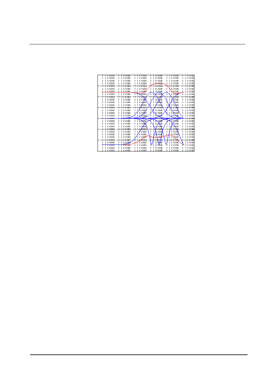
WM8974
Product Preview
w
PP Rev 1.1 September 2004
60
Figure 55 shows the result of having the gain set on more than one channel simultaneously. The
blue traces show each band (lowest cut-off/centre frequency) with
±12dB gain. The red traces show
the cumulative effect of all bands with +12dB gain and all bands -12dB gain, with EQxBW=0 for the
peak filters.
10
-1
10
0
10
1
10
2
10
3
10
4
10
5
-15
-10
-5
0
5
10
15
20
Frequency (Hz)
M
a
gni
t
ude
(
dB
)
Figure 55 Cumulative Frequency Boost/Cut

Product Preview
WM8974
w
PP Rev 1.1 September 2004
61
APPLICATIONS INFORMATION
RECOMMENDED EXTERNAL COMPONENTS
Figure 56 Recommended External Components

WM8974
Product Preview
w
PP Rev 1.1 September 2004
62
PACKAGE DIAGRAM
DM035.B
FL: 24 PIN QFN PLASTIC PACKAGE 4
X
4
X
0.9 mm BODY, 0.50 mm LEAD PITCH
INDEX AREA
(D/2 X E/2)
TOP VIEW
D
E
4
NOTES:
1. DIMENSION b APPLIES TO METALLIZED TERMINAL AND IS MEASURED BETWEEN 0.15 mm AND 0.30 mm FROM TERMINAL TIP.
2. FALLS WITHIN JEDEC, MO-220, VARIATION VGGD-2.
3. ALL DIMENSIONS ARE IN MILLIMETRES.
4. THE TERMINAL #1 IDENTIFIER AND TERMINAL NUMBERING CONVENTION SHALL CONFORM TO JEDEC 95-1 SPP-002.
5. COPLANARITY APPLIES TO THE EXPOSED HEAT SINK SLUG AS WELL AS THE TERMINALS.
6. THIS DRAWING IS SUBJECT TO CHANGE WITHOUT NOTICE.
7. DEPENDING ON THE METHOD OF LEAD TERMINATION AT THE EDGE OF THE PACKAGE, PULL BACK (L1) MAY BE PRESENT.
A3
G
T
H
W
b
Exposed lead
Half etch tie bar
Dimensions (mm)
Symbols
MIN
NOM
MAX
NOTE
A
A1
A3
0.80
0.90
1.00
0.05
0.02
0
0.20 REF
b
D
D2
E
E2
e
L
0.30
0.18
4.00
2.25
2.15
2.00
0.50 BSC
0.30
0.40
0.50
2
2
4.00
2.25
2.15
2.00
0.10
aaa
bbb
ccc
REF:
0.15
0.10
JEDEC, MO-220, VARIATION VGGD-2.
Tolerances of Form and Position
0.25
H
0.1
0.213
G
T
0.1
W
0.2
DETAIL 1
DETAIL 2
E2
A
6
1
13
18
24
19
12
e
D2
b
7
1
B
C
bbb
M
A
BOTTOM VIEW
C
aaa
2 X
C
aaa
2 X
1
C
A3
SEATING PLANE
DETAIL 2
A1
C
0.08
C
ccc
A
5
SIDE VIEW
DETAIL 1
7
AA
DD
CC
BB
L
L1
Dimensions (mm)
Symbols
MIN
NOM
MAX
NOTE
AA
0.235
L1
DD
CC
BB
0.15
0.03
0.181
0.181
0.235
7
7
7
7

Product Preview
WM8974
w
PP Rev 1.1 September 2004
63
IMPORTANT NOTICE
Wolfson Microelectronics plc (WM) reserve the right to make changes to their products or to discontinue any product or
service without notice, and advise customers to obtain the latest version of relevant information to verify, before placing
orders, that information being relied on is current. All products are sold subject to the WM terms and conditions of sale
supplied at the time of order acknowledgement, including those pertaining to warranty, patent infringement, and limitation of
liability.
WM warrants performance of its products to the specifications applicable at the time of sale in accordance with WM's
standard warranty. Testing and other quality control techniques are utilised to the extent WM deems necessary to support
this warranty. Specific testing of all parameters of each device is not necessarily performed, except those mandated by
government requirements.
In order to minimise risks associated with customer applications, adequate design and operating safeguards must be used
by the customer to minimise inherent or procedural hazards. Wolfson products are not authorised for use as critical
components in life support devices or systems without the express written approval of an officer of the company. Life
support devices or systems are devices or systems that are intended for surgical implant into the body, or support or sustain
life, and whose failure to perform when properly used in accordance with instructions for use provided, can be reasonably
expected to result in a significant injury to the user. A critical component is any component of a life support device or system
whose failure to perform can be reasonably expected to cause the failure of the life support device or system, or to affect its
safety or effectiveness.
WM assumes no liability for applications assistance or customer product design. WM does not warrant or represent that any
license, either express or implied, is granted under any patent right, copyright, mask work right, or other intellectual property
right of WM covering or relating to any combination, machine, or process in which such products or services might be or are
used. WM's publication of information regarding any third party's products or services does not constitute WM's approval,
license, warranty or endorsement thereof.
Reproduction of information from the WM web site or datasheets is permissible only if reproduction is without alteration and
is accompanied by all associated warranties, conditions, limitations and notices. Representation or reproduction of this
information with alteration voids all warranties provided for an associated WM product or service, is an unfair and deceptive
business practice, and WM is not responsible nor liable for any such use.
Resale of WM's products or services with statements different from or beyond the parameters stated by WM for that product
or service voids all express and any implied warranties for the associated WM product or service, is an unfair and deceptive
business practice, and WM is not responsible nor liable for any such use.
ADDRESS
Wolfson Microelectronics plc
Westfield House
26 Westfield Road
Edinburgh
EH11 2QB
United Kingdom
Tel :: +44 (0)131 272 7000
Fax :: +44 (0)131 272 7001
Email :: sales@wolfsonmicro.com