WM9703
AC'97 Revision 2.1 Audio Codec
WOLFSON MICROELECTRONICS LTD
w :: www.wolfsonmicro.com
Production Data, September 2001, Rev 3.5
Copyright
2001 Wolfson Microelectronics Ltd.
DESCRIPTION
WM9703 is a high-quality stereo audio codec compliant
with the AC'97 Revision 2.1 specification. It performs full
duplex 18-bit codec functions and supports variable
sample rates from 8 to 48k samples/s and offers excellent
quality with high SNR. Additional features include 3D
sound and line-level outputs. In addition, support is
provided for variable sample rates and accommodation is
made for master/slave mode operation.
WM9703 is interchangeable with AC'97 codecs from
Wolfson and other suppliers. The WM9703 is fully
operable on 3.3V or 5V or mixed 3.3/5V supplies, and is
packaged in the industry standard 48-pin TQFP package
with 7mm-body size.
AC'97 FEATURES
∑
3.3V or 5V operation
∑
18-bit stereo codec
∑
S/N ratio > 95dB
∑
Multiple stereo input mixer
∑
Mono and stereo volume control
∑
48-pin
TQFP
package
∑
Power
management
features
∑
Low power implementation
∑
Very low standby power
AC'97 REVISION 2.1 FEATURES
∑
Variable rate audio (VRA) support
∑
Analogue 3D stereo enhancement
∑
Line level outputs
∑
Supports Revision. 2.1 specified modem sample rates
and filtering
∑
Master/slave ID selection
∑
PC-beep connection when device held reset
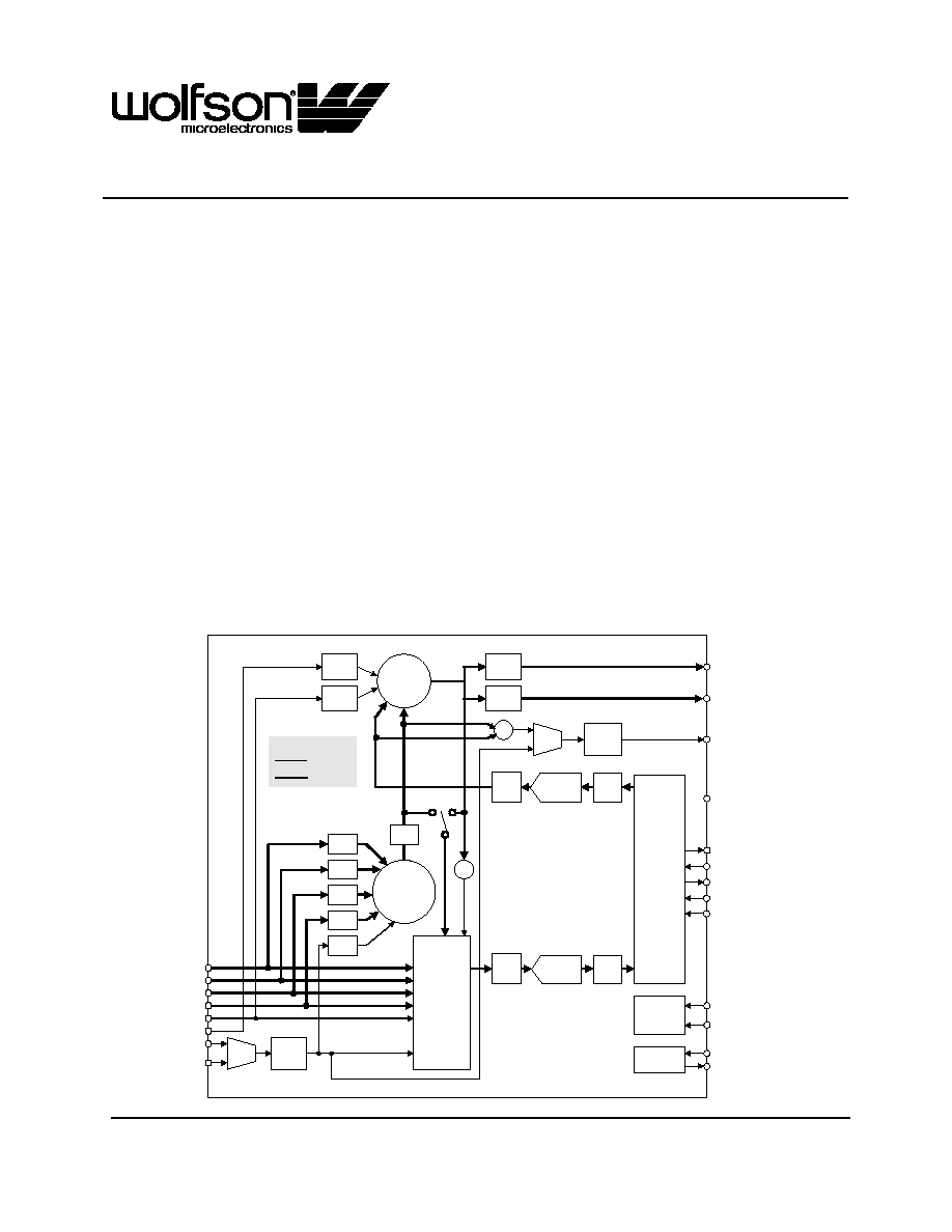
BLOCK DIAGRAM
VOL/
MUTE
VOL/
MUTE
VOL/
MUTE
VOL/
MUTE
VOL/
MUTE
VOL/
MUTE
(37) MONOOUT
(39,41) LNLVLOUT
(35,36) LINEOUT
CD (18,20)
LINEIN (23,24)
VIDEO (16,17)
AUX (14,15)
PHONE (13)
PCBEEP (12)
MIC[1] (21)
MIC[2] (22)
0dB/
20dB
MASTER/
SLAVE
SELECT
(45) CID[0]
(46) CID[1]
(6) BITCLK
(10) SYNC
(8) SDATAIN
(5) SDATAOUT
(11) RESETB
(47) EAPD
VOL/
MUTE
OSC
(2) XTLIN
(3) XTLOUT
VOL
STEREO
DAC
SRC
3D
VOL
STEREO
ADC
SRC
VOL/
MUTE
MUX
VOL/
MUTE
VOL/
MUTE
MUX
KEY:
MONO
STEREO
RECORD
MUX
AND
MUTE
SERIAL
I/F
WM9703
WM9703
Production Data
PD Rev 3.5 September 2001
2
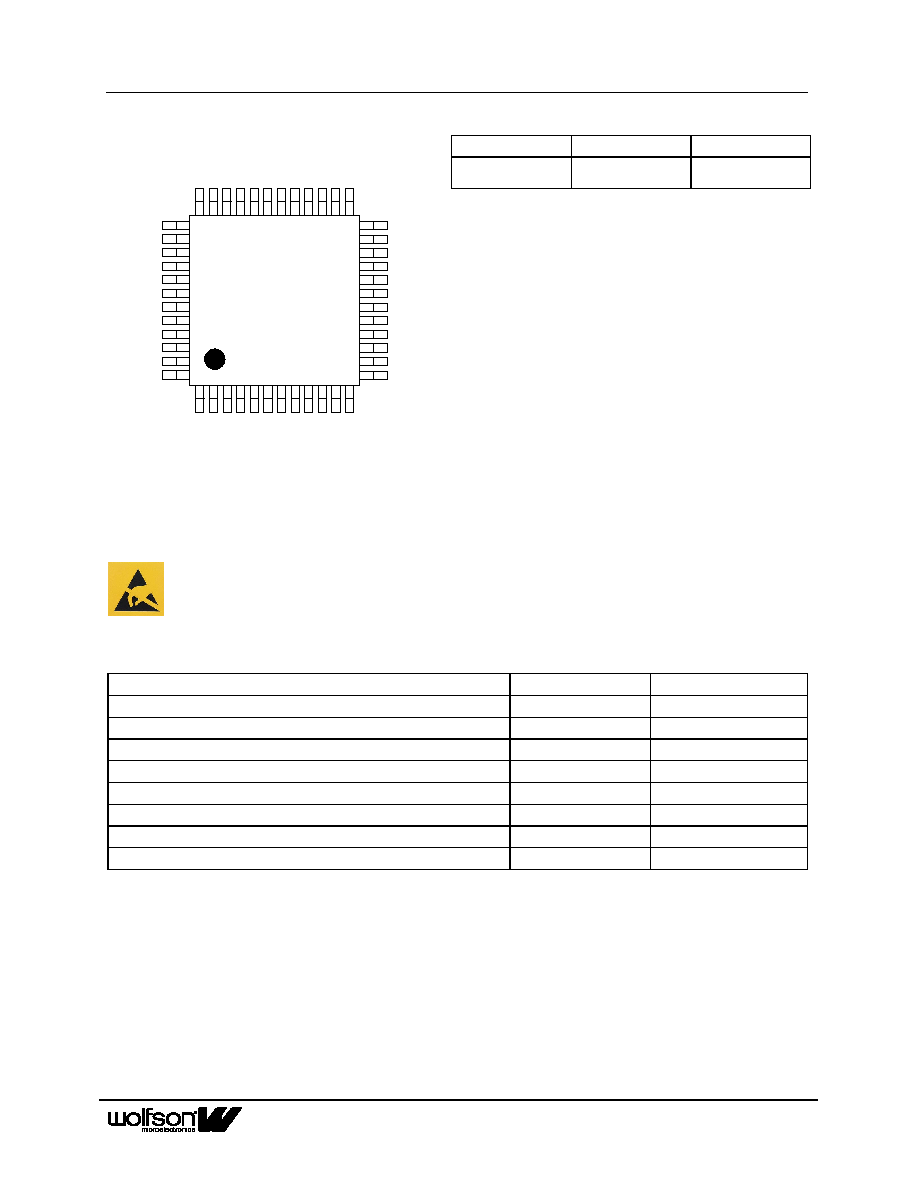
PIN CONFIGURATION
ORDERING INFORMATION
DEVICE
TEMP. RANGE
PACKAGE
WM9703CFT/V
0 to 70
o
C
48-pin TQFP
24
23
16
17
18
19
20
21
22
13
14
15
37
47
46
45
44
43
42
41
40
39
38
48
1
9
8
7
6
5
4
3
2
12
11
10
25
31
30
29
28
27
26
36
35
34
33
32
LINEINR
CDL
MIC2
CDGND
CDR
MIC1
LINEINL
AUXR
PHONE
AUXL
VIDEOL
VIDEOR
DVDD1
DVSS2
BI
TCL
K
SDATAO
UT
DVSS1
XTL
O
UT
XTL
I
N
SDATI
N
DVDD2
SYNC
RESETB
PCBEEP
NC
NC
NC
CID0
CID1
EAPD
MONOOUT
AVDD2
LNLVLOUTL
NC
LNLVLOUTR
AVSS2
LI
N
E
O
U
TR
NC
CAP1
CAP2
CX3
D
1
CX3
D
2
LI
N
E
O
U
TL
AVDD1
AVSS1
VREF
VREFO
U
T
AFI
L
T1
WM9703
ABSOLUTE MAXIMUM RATINGS
Absolute Maximum Ratings are stress ratings only. Permanent damage to the device may be caused by continuously operating
at or beyond these limits. Device functional operating limits and guaranteed performance specifications are given under Electrical
Characteristics at the test conditions specified.
ESD Sensitive Device. This device is manufactured on a CMOS process. It is therefore generically susceptible
to damage from excessive static voltages. Proper ESD precautions must be taken during handling and storage
of this device.
As per specifications IPC/JEDEC J-STD-020A and JEDEC A113-B, this product requires specific storage conditions prior to
surface mount assembly. It has been classified as having a Moisture Sensitivity Level of 2 and as such will be supplied in
vacuum-sealed moisture barrier bags.
CONDITION
MIN
MAX
Digital supply voltage
-0.3V
+7V
Analogue supply voltage
-0.3V
+7V
Voltage range digital inputs
DVSS
-0.3V
DVDD +0.3V
Voltage range analogue inputs
AVDD
-0.3V
AVDD +0.3V
Operating temperature range, T
A
0
o
C
+70
o
C
Storage temperature
-65
o
C
+150
o
C
Package body temperature (soldering 10 seconds)
+240
o
C
Package body temperature (soldering 2 minutes)
+183
o
C
Note:
1.
The digital supply voltage (DVDD) must always be less than or equal to the analogue supply voltage (AVDD).
WM9703
Production Data
PD Rev 3.5 September 2001
3
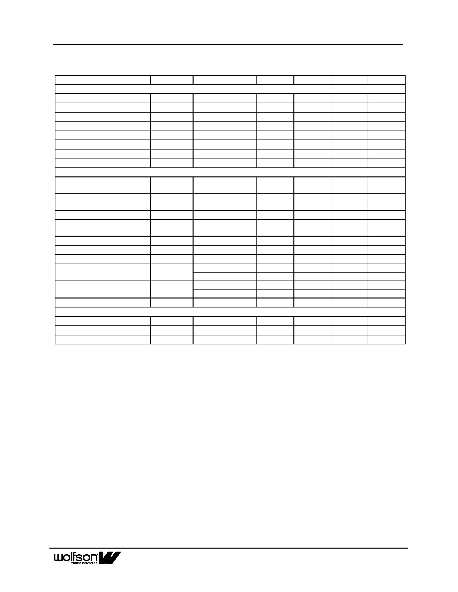
RECOMMENDED OPERATING CONDITIONS
PARAMETER
SYMBOL
TEST CONDITIONS
MIN
TYP
MAX
UNIT
Digital supply range
DVDD1, DVDD2
-10%
3.3 to 5.0
+10%
V
Analogue supply range
AVDD1, AVDD2
-10%
3.3 to 5.0
+10%
V
Digital ground
DVSS1, DVSS2
0
V
Analogue ground
AVSS1, AVSS2
0
V
Difference DVSS to AVSS
-0.3
0
+0.3
V
Analogue supply current
DVDD, AVDD = 5V
35
mA
Digital supply current
DVDD, AVDD = 5V
25
mA
Standby supply current (all PRs set)
DVDD, AVDD = 5V
10
µ
A
Analogue supply current
DVDD, AVDD = 3.3V
22
mA
Digital supply current
DVDD, AVDD = 3.3V
15
mA
Standby supply current (all PRs set)
DVDD, AVDD = 3.3V
6
µ
A
Note:
1.
Both supplies should be powered on and off at the same time
ELECTRICAL CHARACTERISTICS
Test Characteristics:
AVDD = 5V, GND = 0V ..............T
A
= 0
o
C to +70
o
C, unless otherwise stated
DVDD = 3.3V, GND = 0V ..............T
A
= 0
o
C to +70
o
C, unless otherwise stated
PARAMETER
SYMBOL
TEST CONDITIONS
MIN
TYP
MAX
UNIT
Digital Logic Levels (DVDD = 3.3 or 5.0V)
Input LOW level
V
IL
AVSS -0.3
0.8
V
Input HIGH level
V
IH
2.2
AVDD +0.3
V
Output LOW
V
OL
0.1 x DVDD
V
Output HIGH
V
OH
0.9 x DVDD
V
Analogue I/O Levels (Input Signals on any inputs, Outputs on LINEOUT L, R and MONOOUT)
Input level
Minimum input
impedance = 10k
AVSS
-100mV
AVDD
+100mV
V
Output level
Into 10kohm load
AVSS
+100mV
Near rail to
rail
AVDD
-100mV
V
Reference Levels
Reference input/output
CAP2
2/5 AVDD
AVDD/2
3/5 AVDD
V
CAP2 impedance
75
kohms
Mixer reference
VREF
Buffered
CAP2
V
MIC reference
VREFOUT
Buffered
CAP2
V
ADC reference
CAP1
Buffered
CAP2
V
DAC reference
AFILT1
Buffered
CAP2
V
MIDBUFF current sink
(pins CAP1, AFILT2, VREF
and VREFOUT)
AVDD = 5V
-5
-15
mA
MIDBUFF current source
(pins CAP1, AFILT1, VREF
and VREFOUT)
AVDD = 5V
5
15
mA
MIDBUFF current source
(pins CAP1, AFILT1, VREF
and VREFOUT)
AVDD = 3.3V
5
mA
WM9703
Production Data
PD Rev 3.5 September 2001
4
Test Characteristics:
AVDD = 5V, GND = 0V ..............T
A
= 0
o
C to +70
o
C, unless otherwise stated
DVDD = 3.3V, GND = 0V ..............T
A
= 0
o
C to +70
o
C, unless otherwise stated
PARAMETER
SYMBOL
TEST CONDITIONS
MIN
TYP
MAX
UNIT
DAC Circuit Specifications (AVDD = 5V) 48kHz sampling
SNR A-weighted (Note 1)
85
96
dB
Full scale output voltage
VREF
= 2.5V
1.0
Vrms
THD
-3dBFs input
74
90
dB
Frequency response
20
19,200
Hz
Transition band
19,200
28,800
Hz
Stop band
28,800
Hz
Out of band rejection
-40
dB
Spurious tone reduction
-100
dB
PSRR
20 to 20kHz
40
dB
ADC Circuit Specifications (AVDD = 5V) 48kHz sampling
SNR A-weighted (Note 1)
75
85
dB
ADC input for full scale output
VREF
= 2.5V
1.0
Vrms
THD
-6dBV input
74
90
dB
Frequency response
20
19,200
Hz
Transition band
19,200
28,800
Hz
Stop band
28,800
Hz
Stop band rejection
-74
dB
PSRR
20 to 20kHz
40
dB
Mixer Circuit Specifications (AVDD = 5V) 48kHz sampling
SNR CD path A-weighted
(Note 1)
90
100
dB
SNR Other paths A-weighted
(Note 1)
85
95
dB
Maximum input voltage
AVSS
1.0
AVDD
Vrms
Maximum output voltage on
LINEOUT
1.0
1.8
Vrms
THD
0dBV input
74
90
dB
Frequency response (+/-1dB)
20
20,000
Hz
Input impedance (CD inputs)
At any gain
10
15
kohm
At max gain
10
20
kohm
Input impedance (other mixer
inputs)
At 0db gain
100
kohm
At max gain
80
kohm
Input impedance Mic inputs
At 0db gain
10
15
kohm
PSRR
20 to 20kHz
40
dB
DAC Circuit Specifications (AVDD = 3.3V) 48kHz sampling
SNR A-weighted (Note 1)
96
dB
Full scale output voltage
VREF
= 1.65V
0.7
Vrms
THD
3dBFs input
90
dB
Frequency response
20
19,200
Hz
Transition band
19,200
28,800
Hz
Stop band
28,800
Hz
Out of band rejection
-40
dB
Spurious tone reduction
-100
dB
PSRR
20 to 20kHz
40
dB
WM9703
Production Data
PD Rev 3.5 September 2001
5
Test Characteristics:
AVDD = 5V, GND = 0V ..............T
A
= 0
o
C to +70
o
C, unless otherwise stated
DVDD = 3.3V, GND = 0V ..............T
A
= 0
o
C to +70
o
C, unless otherwise stated
PARAMETER
SYMBOL
TEST CONDITIONS
MIN
TYP
MAX
UNIT
ADC Circuit Specifications (AVDD = 3.3V) 48kHz sampling
SNR A-weighted (Note 1)
82
dB
ADC input for full scale output
VREF
= 1.65V
0.7
Vrms
THD
-9dBV input
80
dB
Frequency response
20
19,200
Hz
Transition band
19,200
28,800
Hz
Stop band
28,800
Hz
Stop band rejection
-74
dB
PSRR
20 to 20kHz
40
dB
Mixer Circuit Specifications (AVDD = 3.3V) 48kHz sampling
SNR CD path A-weighted
(Note 1)
97
dB
SNR Other paths A-weighted
(Note 1)
92
dB
Maximum input voltage
0.7
Vrms
Maximum output voltage on
LINEOUT
0.7
Vrms
THD
-3dBV input
90
dB
Frequency response (+/-1dB)
20
20,000
Hz
Input impedance (CD inputs)
At any gain
15
kohm
At max gain
20
kohm
Input impedance (other Mixer
inputs)
At 0db gain
100
kohm
At max gain
80
kohm
Input impedance MIC inputs
At 0db gain
15
kohm
PSRR
20 to 20kHz
40
dB
Clock Frequency Range
Crystal clock
24.576
MHz
BIT_CLK frequency
12.288
MHz
SYNC frequency
48.0
kHz
Note:
1. SNR is the ratio of 0dB signal output level to the output level with no signal, measured A-weighted over a 20Hz to 20kHz
bandwidth.