XECOM
(1)
XE1414L
XE1414L
October 2000
Compact 14.4 KBPS Modem Module for Embedded Applications
Description
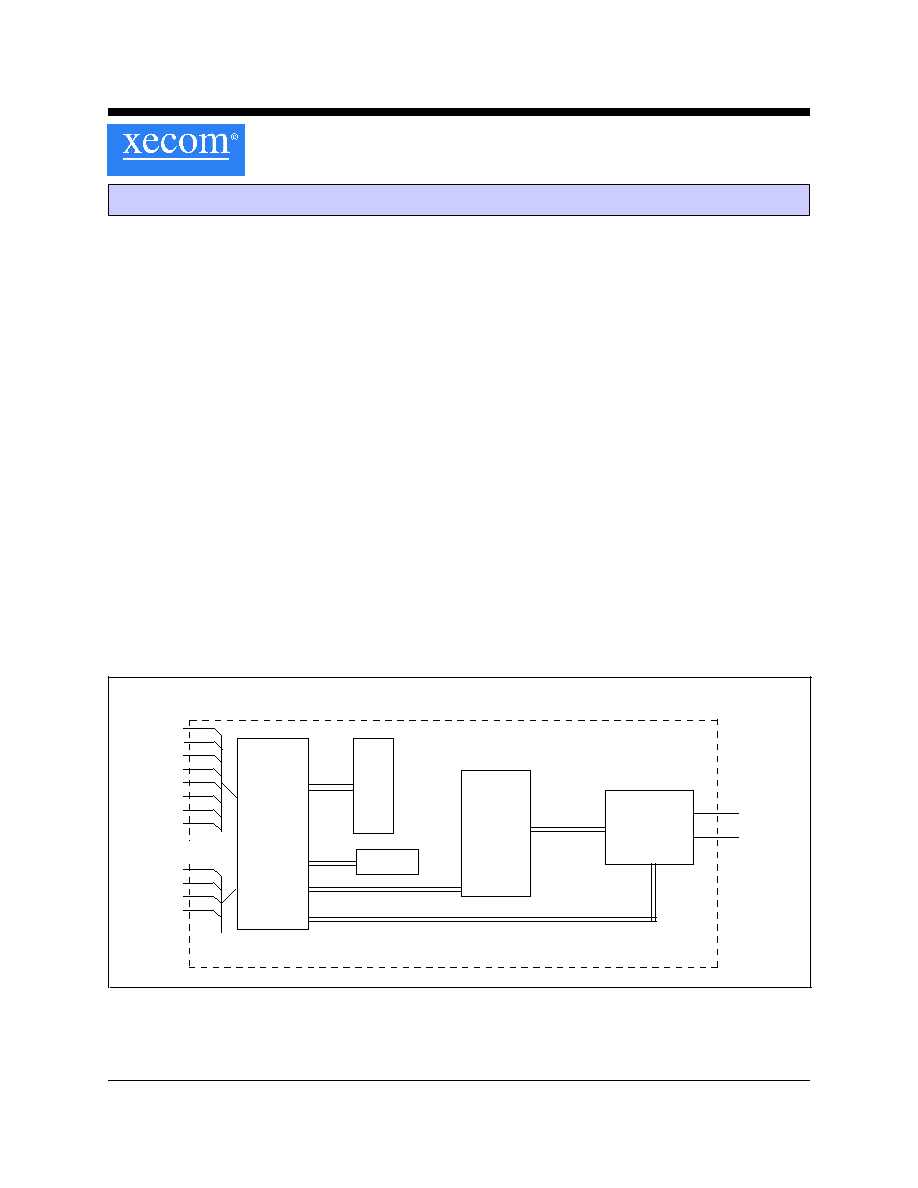
Xecom's XE1414L is a complete, 14.4 Kbps modem in a
single component. The XE1414L can be used in
throughout North America and Japan. It includes user
transferrable FCC Part 68 Registration.
The XE1414L is a complete modem including the DAA.
XE1414L users do not need to add RAM, ROM, Crystals,
low distortion transformer, or switches to complete the
modem design. The user only needs to provide the TTL
level, serial interface and the telephone line connection.
The XE1414L is a full-featured modem. The XE1414L
supports data compression, error correction and fax
transfer. The XE1414L also includes NVRAM for
permanent storage of the modem configuration.
The XE1414L is pin compatible with Xecom's XE3314L,
and XE5614L modems. This family of modems permits a
simple upgrade path from 14,400 bps to 56,000 bps.
Features
*
User Transferrable FCC Part 68 Registration
*
Small Size: 2.75 inches by 1.38 inches by 0.42 inches;
*
Modem Protocols support data transfer from 14.4
KBPS down to 300 BPS: V.32bis, V.32, V.22bis, V.22,
V.21, Bell 212A and 103;
*
Modem Control and Configuration via standard AT
Commands
*
Fax Protocols: V.17, V.29, V.27ter, and V.21 channel 2
*
Error Correction; V.42, MNP2-4 and MNP10
*
Data Compression; V.42bis and MNP5 provides a
maximum effective data rate of 57,600 bps.
*
Non-Volatile Memory for storing telephone numbers
and modem configuration.
* Standard operating temperature range 0C to 70C.
Extended operating temperature range of -40C to +85C
is availalble.
Block Diagram
Modem
Controller
ROM
NVRAM
Analog
Front
End
DAA
/DTR
/RTS
/CTS
/DSR
TXD
RXD
/DCD
Serial I/O
RESET
AR
OH
AMP
Tip
Ring
Auxiliary I/O
XECOM
(2)
XE1414L
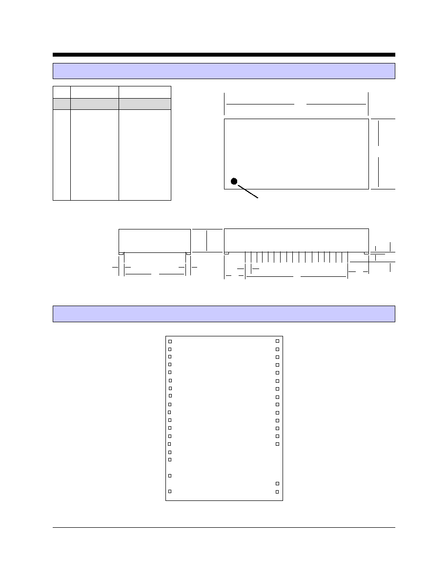
XE1414L PIN CONFIGURATION
NC
AR
RXD
NC
NC
NC
NC
NC
/DTR
NC
/CTS
NC
TXD
/RTS
NC
/RI
TIP
RING
VCC
/DSR
/DCD
NC
RESET
NC
NC
NC
NC
NC
OH
NC
NC
NC
AMP
GND
1
2
3
4
5
6
7
8
9
10
11
12
13
14
15
16
18
20
40
39
38
37
36
35
34
33
32
31
30
29
28
27
22
21
XE1414L Mechanical Specifications
Pins = 0.025 inch square pin; All pins tin-plated
A
2.74
2.760
69.60
70.10
B
1.370
1.390
34.80
35.31
C
0.420
0.430
10.67
10.92
D
1.190
1.210
30.23 30.73
E
1.890
1.910
48.01
48.51
F
0.125
0.200
3.18
5.08
G
0.080
0.100
2.03
2.54
H
0.415
0.435
10.54
11.05
J
0.090
0.110
2.29
2.79
K
0.020
0.025
0.51
0.64
INCHES
METRIC(MM)
PIN
MIN
MAX
MIN
MAX
Denotes Pin 1
A
B
K
F
H
E
J
H
C
D
G
G

XECOM
(3)
XE1414L
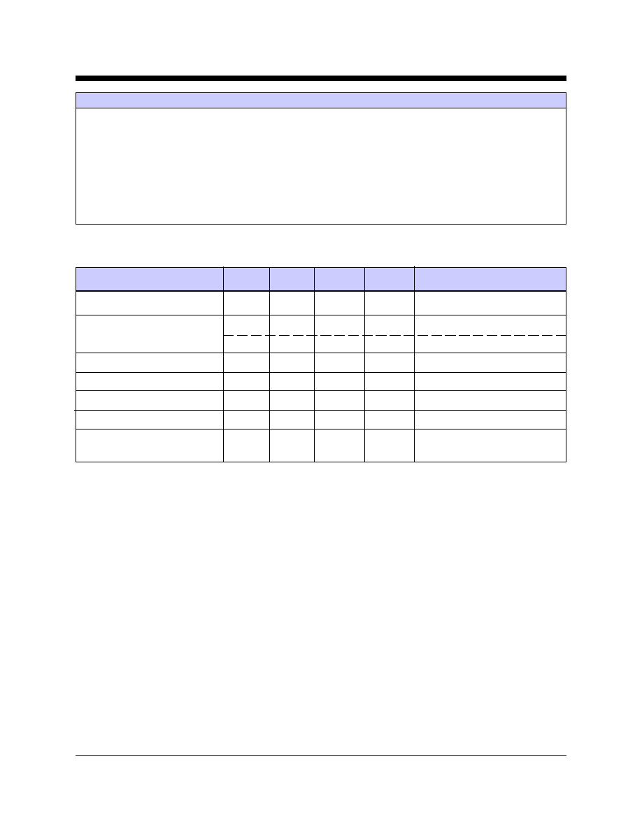
PIN NAME
DESCRIPTION
XE1414L PIN DESCRIPTIONS
1
NC
No Internal Connection
2
AR
Auxiliary Data/Voice Relay, Active High Output, TTL/CMOS. The AR signal goes high when ever the
modem is in the on-hook state. It can be connected to an external relay to switch control of the tele-
phone line between the modem and an auxiliary handset when.
3
RXD
Received Data, Output, TTL. Serial data output to the host. A logic "High" on RXD represents a
"mark" and a logic "Low" represents a "space".
4-8
NC
No Internal Connection
9
\DTR
Data Terminal Ready, Input, active Low, TTL. The "AT&D" command sets the function of \DTR. The
default, AT&D2, requires the host to assert \DTR to permit a modem link. The modem drops the call in
progress if \DTR is revoked and will not connect until \DTR is reasserted.
10
NC
No Internal Connection
11
\CTS
Clear to Send, Output, active Low, TTL/CMOS. \CTS provides the flow control output from the modem
when hardware flow control is selected. The modem revokes \CTS when the modem's input buffer is
full. The modem reasserts \CTS when the buffer can accept more data without a buffer overflow.
12
NC
No Internal Connection
13
TXD
Transmit Data, Input, TTL. Serial data input from the host. A logic "High" represents a "mark" and a
Low represents a "space", TTL.
14
\RTS
Request to Send, input, active Low, TTL. The XE1414L uses \RTS for hardware flow control. When
\RTS is revoked; hardware flow control is enabled, and the modem will not place data on RXD.
15
NC
No Internal Connection
16
\RI
Ring Indicator, Output, active Low, TTL. When low indicates the modem is receiving a ring signal.
18
TIP
Tip connection to the phone line (RJ11 pin 3) from the internal DAA. The XE1414L is not sensitive to
the battery voltage polarity across Tip and Ring.
20
RING
Ring connection to the phone line (RJ11 pin 4) from the internal DAA.
21
GND
Ground (0 volts)
22
AMP
Audio Output function is set by L & M commands and the value in register S22. This output can drive a
minimum load of 300 ohms.
27-29
N/C
No Internal Connection
30
OH
Off-Hook, Output, active High. OH indicates the modem's hookswitch relay is closed. Hookswitch clo-
sure connects the modem to the telephone line. This signal is available only on the XE1414L.
31-35
N/C
No Internal Connection
36
RESET
Hardware reset pin, Input, active High, TTL. A high on Pin 36 initiates a hardware reset. An external
reset is not required or recommended. The Reset pulse must be held a minimum of 100 milliseconds.
37
N/C
No Internal Connection
38
\DCD
Data Carrier Detect, Output Active Low, TTL/CMOS. The &C command sets the function of \DCD. In
the default state \DCD activates when a valid carrier is detected.
39
\DSR
Data Set Ready, Output, active Low, TTL/CMOS. &S sets the \DSR function. In the default condition,
AT&S0, \DSR is forced true.
40
Vcc
+5 Volts
XECOM
(4)
XE1414L
Parameter
Min
Typ
Max
Units
Comments
XE1414L ELECTRICAL SPECIFICATIONS
VCC
4.75
5.25
Volts
ICC
130
140
160
ma
On Line
45
Sleep Mode
Ring Voltage Detected
38
150
RMS
Type B Ringer
Ring Frequency Detected
15.3
68
Hz
Type B Ringer
Telephone Loop Current
20
100
ma
Off-Hook
Data Transmit level
-12
-10.5
-9.0
dBm
DTMF Transmit Level
-2.5
0
dBm
Avg over 3 second interval
SUPPLY VOLTAGE - Vcc
+6.5 Volts
DC INPUT VOLTAGE
-0.6 Volts to +6.5 Volts
STORAGE TEMPERATURE RANGE
-25� C TO +85� C
LEAD TEMPERATURE (Soldering, 2 sec per wave)
260� C
OPERATING TEMPERATURE RANGE
0 TO 70� C
*Exceeding these values may result in permanent damage to the device.
XE1414L ABSOLUTE MAXIMUM RATINGS
XECOM
(5)
XE1414L
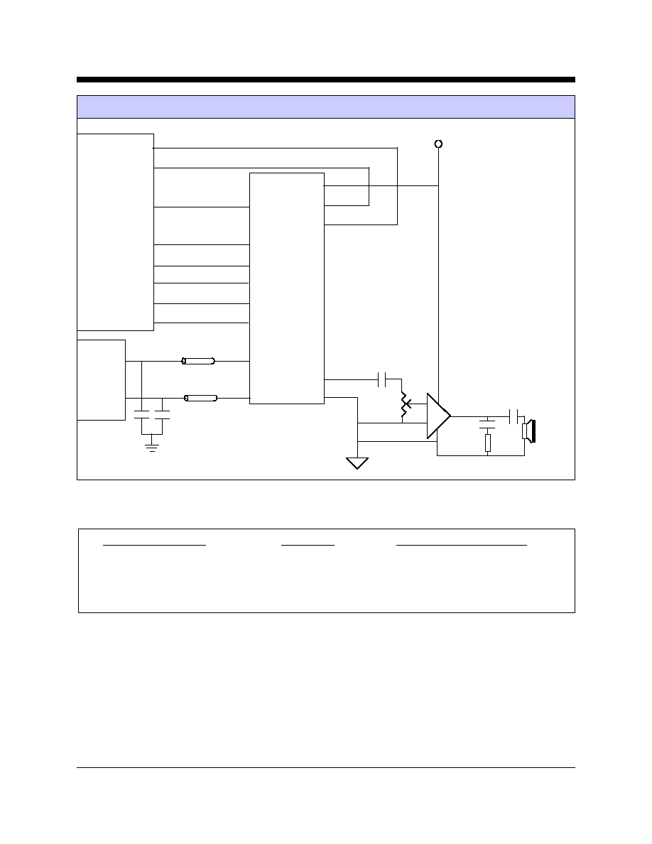
XE1414L Typical Connection Diagram
16C550
UART
XE1414L
/DCD
/DSR
SIN
/DTR
/CTS
SOUT
/RTS
/RI
RXD
/DTR
/CTS
TXD
/RTS
/RI
TIP
RING
VCC
/DSR
/DCD
AMP
GND
C1
C2
RJ11
3
4
FB1
FB2
+ 5 Volts
LM386
.05 ufd
10 ohms
250 ufd
8 ohm,
.5 W
speaker
.2 ufd
50K
Note: RJ11 Pin assignments reflect a 6-pin connector. Tip and Ring are always the center pins of the RJ11 Jack.
Recommended Parts
Reference Designation
Description
Recommended Part Number
FB1, FB2
Ferrite Beads
TDK ACB2012L-120-X
C1, C2
470 pfd 2600 VAC Capacitors
Panasonic ECKDR471
J1
RJ11 Jack
Stewart SS6446NF