Cool Solutions for Wireless Connectivity
XEMICS SA
∑
e-mail: info@xemics.com
∑
web: www.xemics.com
Data Sheet
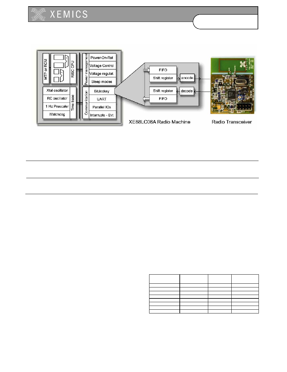
XE88LC06A
XE88LC06A
Ultra Low-Power Low-Voltage
Radio Machine
General Description
The XE88LC06A is an ultra low-power low-voltage
microcontroller based Radio Machine. It includes the
revolutionary BitJockey, UART type of peripheral
specialized for radio communication.
XE88LC06A is available with on chip ROM or Multiple-
Time-Programmable (MTP) program memory.
Key product Features
∑
Ultra low-power MCU, up to 7 MIPS
∑
300 uA at 1 MIPS operation
∑
6 uA at 32 kHz operation
∑
1 uA time keeping
∑
Low-voltage operation (1.2 - 5.5 V supply voltage)
∑
22 kB (8 kW) ROM/MTP, 512 B RAM
∑
4
counters
∑
PWM,
UART,
BitJockeyTM
∑
Analog
matrix
switching
∑
4 low-power analog comparators
∑
independant RC and crystal oscillators
∑
5 reset, 15 interrupt, 8 event sources
∑
100 years MTP Flash retention at 55∞C
Applications
∑
RF companion chip
∑
RF system supervisor
∑
Portable, battery operated instruments
∑
Metering
∑
Remote
control
∑
HVAC
control
Ordering Information
Product
Temperature
range
Memory
type
Package
XE88LC06AMI000
-40∞C to 85 ∞C
MTP
die
XE88LC06AMI014
-40∞C to 85 ∞C
MTP
SO24
XE88LC06AMI015
-40∞C to 85 ∞C
MTP
SO28
XE88LC06AMI026
-40∞C to 85 ∞C
MTP
TQFP32
XE88LC06ARI000
-40∞C to 125∞C
ROM
die
XE88LC06ARI014
-40∞C to 125∞C
ROM
SO24
XE88LC06ARI015
-40∞C to 125∞C
ROM
SO28
XE88LC06ARI026
-40∞C to 125∞C
ROM
TQFP32

D0303-136
Datasheet
XE88LC06A
TABLE OF CONTENTS
Chapter Title
1. General
overview
2. XE88LC06A
performance
3. CPU
4. Memory
mapping
5.
Low power modes
6. Reset
generator
7. Clock
generation
8. Interrupt
handler
9. Event
handler
10.
Low power RAM
11. Port
A
12. Port
B
13. Port
D
14.
Radio Asynchronous Receiver/Transmitter (BitJockeyTM)
15.
Universal Asynchronous Receiver/Transmitter (UART)
16.
Universal Synchronous Receiver/Transmitter (USRT)
17. Counters/PWM
18.
The Voltage Level Detector
19.
Low power comparators
20. Dimensions

1-2
D0303-136
Datasheet
XE88LC06A
1.1 Top schematic
The top level block schematic of the circuit is shown in Figure 1-1. The heart of the circuit consists of
the Coolrisc816 CPU (central processing unit) core. This core includes an 8x8 multiplier and 16
internal registers.
The bus controller generates all control signals for access to all data registers other than the CPU
internal registers.
The reset block generates the adequate reset signals for the rest of the circuit as a function of the set-
up contained in its control registers. Possible reset sources are the power-on-reset (POR), the
external pin NRESET, the watchdog (WD), a bus error detected by the bus controller or a
programmable pattern on Port A.
The clock generation and power management block sets up the clock signals and generates internal
supplies for different blocks. The clock can be generated from the RC oscillator (this is the start-up
condition), the crystal oscillator (XTAL) or an external clock source (given on the XIN pin).
The test controller generates all set-up signals for different test modes. In normal operation, it is used
as a set of 8 low power RAM. If power consumption is important for the application, the variables that
need to be accessed frequently should be stored in these registers rather than in the RAM.
The IRQ handler routes the interrupt signals of the different peripherals to the IRQ inputs of the CPU
core. It allows masking of the interrupt sources and it flags which interrupt source is active.
Events are generally used to restart the processor after a HALT period without jumping to a specified
address, i.e. the program execution resumes with the instruction following the HALT instruction. The
EVN handler routes the event signals of the different peripherals to the EVN inputs of the CPU core. It
allows masking of the event sources and it flags which event source is active.
The Port B is an 8 bit parallel IO port with analog capabilities. The USRT, UART, PWM and CMPD
blocks also make use of this port.
The instruction memory is a 22-bit wide flash or ROM memory depending on the circuit version. In
case of the ROM version, the UPP pin is not used. The maximal number of instructions in this product
is 8192.
The data memory on this product is a 512 byte SRAM.
The port A is an 8 bit parallel input port. It can also generate interrupts, events or a reset. It can be
used to input external clocks for the timer/counter/PWM block.
The Port D is a general purpose 8 bit parallel IO port.
The USRT (universal synchronous receiver/transmitter) contains some simple hardware functions in
order to simplify the software implementation of a synchronous serial link.
The UART (universal asynchronous receiver/transmitter) contains a full hardware implementation of
the asynchronous serial link.
The RFIF interface is a serial interface dedicated to communication with RF circuits. From the CPU
side, it very much looks like an ordinary UART but it also implements low level coding/decoding and
frame synchronisation. The input/output pins are multiplexed on port D.
The counters/timers/PWM can take its clocks from internal or external sources (on Port A) and can
generate interrupts or events. The PWM is output on Port B.

1-3
D0303-136
Datasheet
XE88LC06A
The VLD (voltage level detector) detects the battery end of life with respect to a programmable
threshold.
The CMPD contains a 4 channel comparator. It is intended to monitor analog or digital signals whilst
having a very low power consumption.
INSTRUCTION MEMORY
B
U
S
C
O
N
T
R
O
L
L
E
R
TEST CONTROLLER
RESET BLOCK
WD
CLOCK
GENERATION/
POW ER
MANAGEMENT
VREG
XTAL
RC
CPU
COOLRISC816
8
X
8
MULTIPLIER
16 CPU
REGISTERS
IRQ HANDLING
EVN HANDLING
PORT B
8 DATA REGISTERS
PORT A
USRT
PORT D
address
control
datain
dataout
reset
control
clocks
test
control
irq
evn
VPP
VBAT
VSS
NRESET
XIN
XOUT
VREG
TEST
PB(7:0)
PA(7:0)
PD(7:0)
DATA
MEMORY
UART
COUNTERS
TIMERS
PW M
VLD
CMPD
P
B
(
5:
4)
P
B
(
7:
6)
P
A
(
3:
0)
PB(
1:0
)
P
B
(
7:
4)
POR
RFIF
BitJockey
PD
(3
:0
)
Figure 1-1. Block schematic of the XE88LC06A circuit.