DS002 (v1.5) December 5, 2001
www.xilinx.com
1
Preliminary Product Specification
1-800-255-7778
© 2001 Xilinx, Inc. All rights reserved. All Xilinx trademarks, registered trademarks, patents, and disclaimers are as listed at
http://www.xilinx.com/legal.htm
.
All other trademarks and registered trademarks are the property of their respective owners. All specifications are subject to change without notice.
7
Features
∑
Certified to MIL-PRF-38535 (Qualified Manufacturer
Listing)
∑
Guaranteed over the full military temperature range
(≠55
∞
C to +125
∞
C)
∑
Ceramic and Plastic Packages
∑
Fast, high-density Field-Programmable Gate Arrays
-
Densities from 100K to 1M system gates
-
System performance up to 200 MHz
-
Hot-swappable for Compact PCI
∑
Multi-standard SelectI/OTM interfaces
-
16 high-performance interface standards
-
Connects directly to ZBTRAM devices
∑
Built-in clock-management circuitry
-
Four dedicated delay-locked loops (DLLs) for
advanced clock control
-
Four primary low-skew global clock distribution
nets, plus 24 secondary global nets
∑
Hierarchical memory system
-
LUTs configurable as 16-bit RAM, 32-bit RAM,
16-bit dual-ported RAM, or 16-bit Shift Register
-
Configurable synchronous dual-ported 4K-bit
RAMs
-
Fast interfaces to external high-performance RAMs
∑
Flexible architecture that balances speed and density
-
Dedicated carry logic for high-speed arithmetic
-
Dedicated multiplier support
-
Cascade chain for wide-input functions
-
Abundant registers/latches with clock enable, and
dual synchronous/asynchronous set and reset
-
Internal 3-state bussing
-
IEEE 1149.1 boundary-scan logic
-
Die-temperature sensing device
∑
Supported by FPGA FoundationTM and Alliance
Development Systems
-
Complete support for Unified Libraries, Relationally
Placed Macros, and Design Manager
-
Wide selection of PC and workstation platforms
∑
SRAM-based in-system configuration
-
Unlimited reprogrammability
-
Four programming modes
∑
0.22
µ
m 5-layer metal process
∑
100% factory tested
∑
Available to Standard Microcircuit Drawings
-
5962-99572 for XQV300
-
5962-99573 for XQV600
-
5962-99574 for XQV1000
-
Contact Defense Supply Center Columbus (DSCC)
for more information at
http://www.dscc.dla.mil
Description
The QProTM VirtexTM FPGA family delivers high-perfor-
mance, high-capacity programmable logic solutions. Dra-
matic increases in silicon efficiency result from optimizing
the new architecture for place-and-route efficiency and
exploiting an aggressive 5-layer-metal 0.22
µ
m CMOS pro-
cess. These advances make QPro Virtex FPGAs powerful
and flexible alternatives to mask-programmed gate arrays.
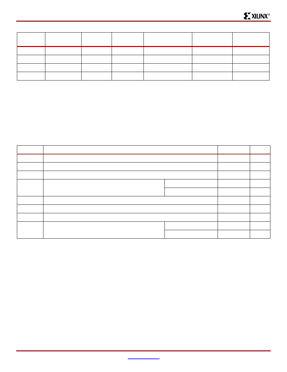
The Virtex family comprises the four members shown in
Table 1
.
Building on experience gained from previous generations of
FPGAs, the Virtex family represents a revolutionary step
forward in programmable logic design. Combining a wide
variety of programmable system features, a rich hierarchy of
fast, flexible interconnect resources, and advanced process
technology, the QPro Virtex family delivers a high-speed
and high-capacity programmable logic solution that
enhances design flexibility while reducing time-to-market.
Refer to the
"VirtexTM 2.5V Field Programmable Gate
Arrays"
commercial data sheet for more information on
device architecture and timing specifications.
0
QPro
Virtex 2.5V QML
High-Reliability FPGAs
DS002 (v1.5) December 5, 2001
0
2
Preliminary Product Specification
R
QPro Virtex 2.5V QML High-Reliability FPGAs
2
www.xilinx.com
DS002 (v1.5) December 5, 2001
1-800-255-7778
Preliminary Product Specification
R
Virtex Electrical Characteristics
Based on preliminary characterization. Further changes are not expected.
All specifications are representative of worst-case supply voltage and junction temperature conditions. The parameters
included are common to popular designs and typical applications. Contact the factory for design considerations requiring
more detailed information.
Virtex DC Characteristics
Absolute Maximum Ratings
Table 1: QPro Virtex Field-Programmable Gate Array Family Members
Device
System Gates
CLB Array
Logic Cells
Maximum
Available I/O
Block RAM Bits
Max Select
RAM Bits
XQV100
108,904
20 x 30
2,700
180
40,960
38,400
XQV300
322,970
32 x 48
6,912
316
65,536
98,304
XQV600
661,111
48 x 72
15,552
316
98,304
221,184
XQV1000
1,124,022
64 x 96
27,648
404
131,072
393,216
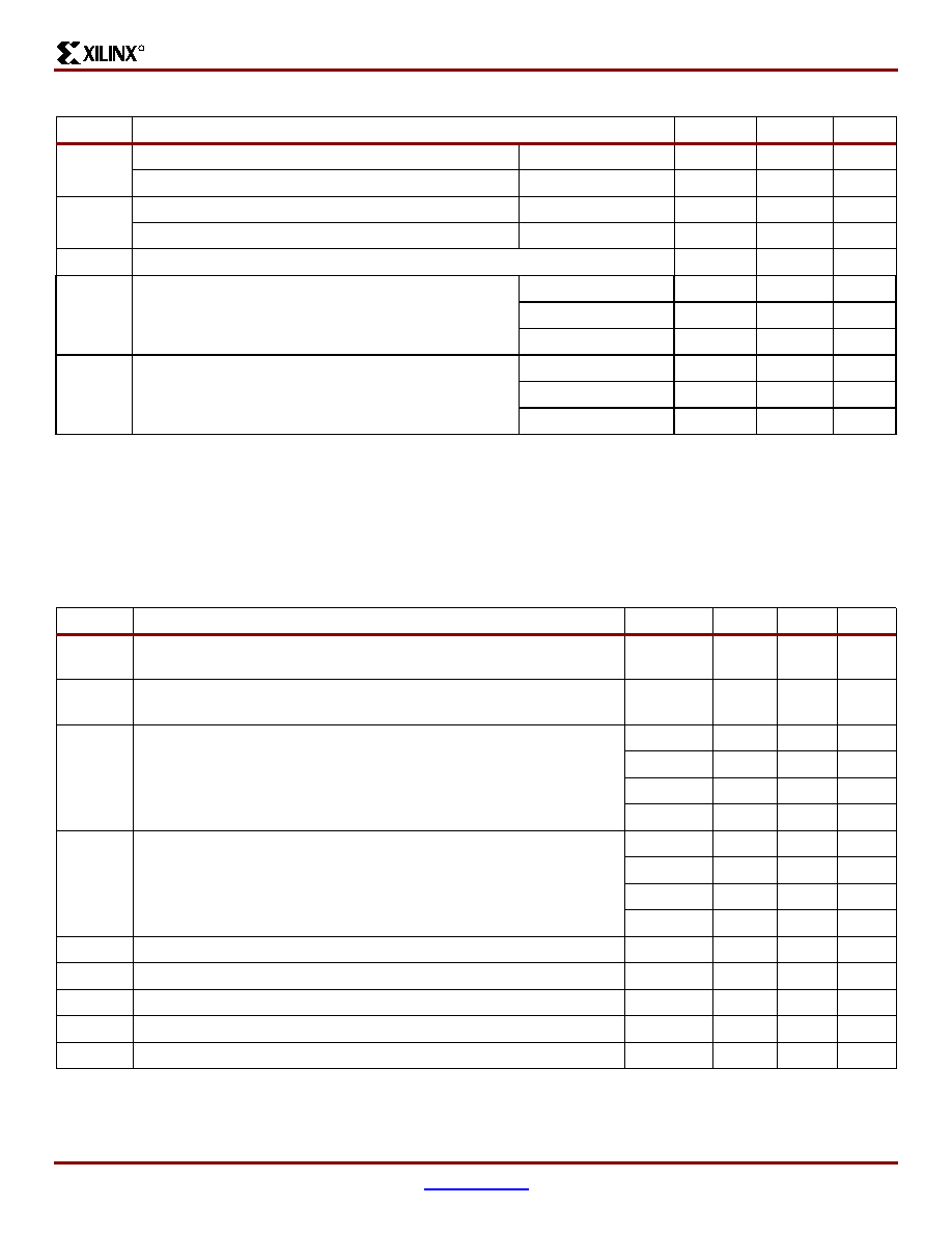
Symbol
Description Min/Max
Units
V
CCINT
Supply voltage relative to GND
≠0.5 to 3.0
V
V
CCO
Supply voltage relative to GND
≠0.5 to 4.0
V
V
REF
Input reference Voltage
≠0.5 to 3.6
V
V
IN
(3)
Input voltage relative to GND
Using V
REF
≠0.5 to 3.6
V
Internal threshold
≠0.5 to 5.5
V
V
TS
Voltage applied to 3-state output
≠0.5 to 5.5
V
V
CC
Longest supply voltage rise time from 1V to 2.375V
50
ms
T
STG
Storage temperature (ambient)
≠65 to +150
∞
C
T
J
Junction temperature
Ceramic packages
+150
∞
C
Plastic packages
+125
∞
C
Notes:
1.
Stresses beyond those listed under Absolute Maximum Ratings may cause permanent damage to the device. These are stress
ratings only, and functional operation of the device at these or any other conditions beyond those listed under Operating Conditions
is not implied. Exposure to Absolute Maximum Ratings conditions for extended periods of time may affect device reliability.
2.
Power supplies may turn on in any order.
3.
For protracted periods (e.g., longer than a day), V
IN
should not exceed V
CCO
by more that 3.6V.
QPro Virtex 2.5V QML High-Reliability FPGAs
DS002 (v1.5) December 5, 2001
www.xilinx.com
3
Preliminary Product Specification
1-800-255-7778
R
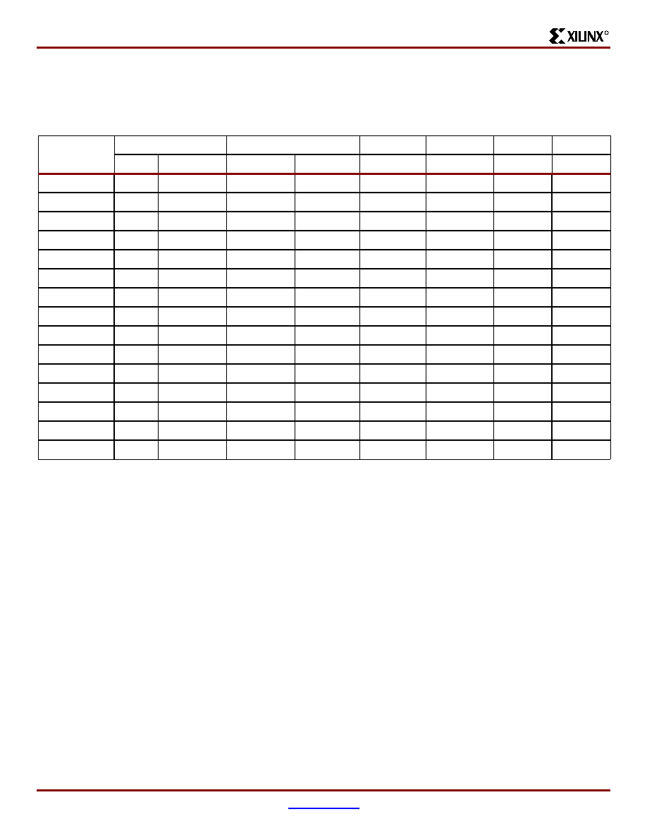
Recommended Operating Conditions
DC Characteristics Over Recommended Operating Conditions
Symbol
Description
Min
Max
Units
V
CCINT
Supply voltage relative to GND, T
C
= ≠55
∞
C to +125
∞
C
Ceramic packages
2.5 ≠ 5%
2.5 + 5%
V
Supply voltage relative to GND, T
J
= ≠55
∞
C to +125
∞
C
Plastic packages
2.5 ≠ 5%
2.5 + 5%
V
V
CCO
Supply voltage relative to GND, T
C
= ≠55
∞
C to +125
∞
C
Ceramic packages
1.2
3.6
V
Supply voltage relative to GND, T
J
= ≠55
∞
C to +125
∞
C
Plastic packages
1.2
3.6
V
T
IN
Input signal transition time
-
250
ns
T
IC
Initialization Temperature Range
(4)
XQVR300
≠55
+125
∞
C
XQVR600
≠55
+125
∞
C
XQVR1000
≠40
+125
∞
C
T
OC
Operational Temperature Range
(5)
XQVR300
≠55
+125
∞
C
XQVR600
≠55
+125
∞
C
XQVR1000
≠55
+125
∞
C
Notes:
1.
Correct operation is guaranteed with a minimum V
CCINT
of 2.25V (Nominal V
CCINT
≠ 10%). Below the minimum value stated above,
all delay parameters increase by 3% for each 50 mV reduction in V
CCINT
below the specified range.
2.
At junction temperatures above those listed as Operating Conditions, all delay parameters increase by 0.35% per
∞
C.
3.
Input and output measurement threshold is ~50% of V
CC
.
4.
Initialization occurs from the moment of V
CC
ramp-up to the rising transition of the INIT pin.
5.
The device is operational after the INIT pin has transitioned high.
Symbol
Description
Device
Min
Max
Units
V
DRINT
Data retention V
CCINT
voltage
(below which configuration data may be lost)
All
2.0
-
V
V
DRIO
Data retention V
CCO
voltage
(below which configuration data may be lost)
All
1.2
-
V
I
CCINTQ
Quiescent V
CCINT
supply current
(1)
XQV100
-
50
mA
XQV300
-
75
mA
XQV600
-
100
mA
XQV1000
-
100
mA
I
CCOQ
Quiescent V
CCINT
supply current
(1)
XQV100
-
2
mA
XQV300
-
2
mA
XQV600
-
2
mA
XQV1000
-
2
mA
I
REF
V
REF
current per V
REF
pin
-
-
20
µ
A
I
L
Input or output leakage current
-
≠10
+10
µ
A
C
IN
Input capacitance (sample tested)
-
-
8
pF
I
RPU
Pad pull-up (when selected) at V
IN
= 0V, V
CCO
= 3.3V (sample tested)
-
(2)
0.25
mA
I
RPD
Pad pull-down (when selected) at V
IN
= 3.6V (sample tested)
-
(2)
0.15
mA
Notes:
1.
With no output current loads, no active input pull-up resistors, all I/O pins in a High-Z state and floating.
2.
Internal pull-up and pull-down resistors guarantee valid logic levels at unconnected input pins. These pull-up and pull-down resistors
do not guarantee valid logic levels when input pins are connected to other circuits.
QPro Virtex 2.5V QML High-Reliability FPGAs
4
www.xilinx.com
DS002 (v1.5) December 5, 2001
1-800-255-7778
Preliminary Product Specification
R
DC Input and Output Levels
Values for V
IL
and V
IH
are recommended input voltages.
Values for I
OL
and I
OH
are guaranteed output currents over
the recommended operating conditions at the V
OL
and V
OH
test points. Only selected standards are tested. These are
chosen to ensure that all standards meet their specifica-
tions. The selected standards are tested at minimum V
CCO
with the respective V
OL
and V
OH
voltage levels shown.
Other standards are sample tested.
Input/Output
Standard
V
IL
V
IH
V
OL
V
OH
I
OL
I
OH
V, min
V, max
V, min
V, max
V, max
V, min
mA
mA
LVTTL
(1)
≠0.5
0.8
2.0
5.5
0.4
2.4
24
≠24
LVCMOS2
≠0.5
0.7
1.7
5.5
0.4
1.9
12
≠12
PCI, 3.3V
≠0.5
44% V
CCINT
60% V
CCINT
V
CCO
+ 0.5
10% V
CCO
90% V
CCO
(2)
(2)
PCI, 5.0V
≠0.5
0.8
2.0
5.5
0.55
2.4
(2)
(2)
GTL
≠0.5
V
REF
≠ 0.05
V
REF
+ 0.05
3.6
0.4
n/a
40
n/a
GTL+
≠0.5
V
REF
≠ 0.1
V
REF
+ 0.1
3.6
0.6
n/a
36
n/a
HSTL I
≠0.5
V
REF
≠ 0.1
V
REF
+ 0.1
3.6
0.4
V
CCO
≠ 0.4
8
-8
HSTL III
≠0.5
V
REF
≠ 0.1
V
REF
+ 0.1
3.6
0.4
V
CCO
≠ 0.4
24
≠8
HSTL IV
≠0.5
V
REF
≠ 0.1
V
REF
+ 0.1
3.6
0.4
V
CCO
≠ 0.4
48
≠8
SSTL3 I
≠0.5
V
REF
≠ 0.2
V
REF
+ 0.2
3.6
V
REF
≠ 0.6
V
REF
+ 0.6
8
≠8
SSTL3 II
≠0.5
V
REF
≠ 0.2
V
REF
+ 0.2
3.6
V
REF
≠ 0.8
V
REF
+ 0.8
16
≠16
SSTL2 I
≠0.5
V
REF
≠ 0.2
V
REF
+ 0.2
3.6
V
REF
≠ 0.65
V
REF
+ 0.65
7.6
≠7.6
SSTL2 II
≠0.5
V
REF
≠ 0.2
V
REF
+ 0.2
3.6
V
REF
≠ 0.80
V
REF
+ 0.80
15.2
≠15.2
CTT
≠0.5
V
REF
≠ 0.2
V
REF
+ 0.2
3.6
V
REF
≠ 0.4
V
REF
+ 0.4
8
≠8
AGP
≠0.5
V
REF
≠ 0.2
V
REF
+ 0.2
3.6
10% V
CCO
90% V
CCO
(2)
(2)
Notes:
1.
V
OL
and V
OH
for lower drive currents are sample tested.
2.
Tested according to the relevant specifications.
QPro Virtex 2.5V QML High-Reliability FPGAs
DS002 (v1.5) December 5, 2001
www.xilinx.com
5
Preliminary Product Specification
1-800-255-7778
R
Virtex Switching Characteristics
Testing of switching parameters is modeled after testing
methods specified by MIL-M-38510/605. All devices are
100% functionally tested. Internal timing parameters are
derived from measuring internal test patterns. Listed below
are representative values. For more specific, more precise,
and worst-case guaranteed data, use the values reported
by the static timing analyzer (TRCE in the Xilinx Develop-
ment System) and back-annotated to the simulation netlist.
All timing parameters assume worst-case operating condi-
tions (supply voltage and junction temperature). Values
apply to all Virtex devices unless otherwise noted.
IOB Input Switching Characteristics
Input delays associated with the pad are specified for
LVTTL levels. For other standards, adjust the delays with
the values shown in
"IOB Input Switching Characteristics
Standard Adjustments" on page 6
.
Symbol
Description
Device
Speed Grade
Units
-4
Min
Max
Propagation Delays
T
IOPI
Pad to I output, no delay
All
-
1.0
ns
T
IOPID
Pad to I output, with delay
XQV100
-
1.9
ns
XQV300
-
1.9
ns
XQV600
-
2.3
ns
XQV1000
-
2.7
ns
T
IOPLI
Pad to output IQ via transparent latch, no
delay
All
-
2.0
ns
T
IOPLID
Pad to output IQ via transparent latch, with
delay
XQV100
-
4.8
ns
XQV300
-
5.1
ns
XQV600
-
5.5
ns
XQV1000
-
5.9
ns
Sequential Delays
T
IOCKIQ
Clock CLK to output IQ
All
-
0.8
ns
Setup and Hold Times with Respect to Clock CLK
Setup Time / Hold Time
T
IOPICK
/ T
IOICKP
Pad, no delay
All
2.0 / 0
-
ns
T
IOPICKD
/ T
IOICKPD
Pad, with delay
All
5.0 / 0
-
ns
T
IOICECK
/ T
IOCKICE
ICE input
All
1.0 / 0
-
ns
T
IOSRCKI
/ T
IOCKISR
SR input (IFF, synchronous)
All
1.3 / 0
-
ns
Set/Reset Delays
T
IOSRIQ
SR input to IQ (asynchronous)
All
-
1.8
ns
T
GSRQ
GSR to output IQ
All
-
12.5
ns
Notes:
1.
A Zero "0" Hold Time listing indicates no hold time or a negative hold time. Negative values can not be guaranteed "best-case",
but if a "0" is listed, there is no positive hold time.