
DS012 (v1.7) June 23, 2003
www.xilinx.com
1
Preliminary Product Specification
1-800-255-7778
© 2003 Xilinx, Inc. All rights reserved. All Xilinx trademarks, registered trademarks, patents, and disclaimers are as listed at
http://www.xilinx.com/legal.htm
.
All other trademarks and registered trademarks are the property of their respective owners. All specifications are subject to change without notice.
Features
∑
Fast Zero PowerTM (FZP) design technique provides
ultra-low power and very high speed
∑
Innovative XPLA3 architecture combines high speed
with extreme flexibility
∑
Based on industry's first TotalCMOS PLD -- both
CMOS design and process technologies
∑
Advanced 0.35
µ
five layer metal EEPROM process
-
1,000 erase/program cycles guaranteed
-
20 years data retention guaranteed
∑
3V, In-System Programmable (ISP) using JTAG IEEE
1149.1 interface
-
Full Boundary Scan Test (IEEE 1149.1)
-
Fast programming times
∑
Ultra-low static power of less than 100
µ
A
∑
Support for complex asynchronous clocking
-
16 product term clocks and four local control term
clocks per function block
-
Four global clocks and one universal control term
clock per device
∑
Excellent pin retention during design changes
∑
Available in commercial grade and extended voltage
(2.7V to 3.6V) industrial grade
∑
5V tolerant I/O pins
∑
Input register set up time of 2.5 ns
∑
Single pass logic expandable to 48 product terms
∑
High-speed pin-to-pin delays of 5.0 ns
∑
Slew rate control per output
∑
100% routable
∑
Security bit prevents unauthorized access
∑
Supports hot-plugging capability
∑
Design entry/verification using Xilinx or industry
standard CAE tools
∑
Innovative Control Term structure provides:
-
Asynchronous macrocell clocking
-
Asynchronous macrocell register preset/reset
-
Clock enable control per macrocell
∑
Four output enable controls per function block
∑
Foldback NAND for synthesis optimization
∑
Universal 3-state which facilitates "bed of nails" testing
∑
Available in Chip-scale BGA, Fineline BGA, PLCC, and
QFP package
0
CoolRunner XPLA3 CPLD
DS012 (v1.7) June 23, 2003
0
14
Preliminary Product Specification
R
Table 1: CoolRunner XPLA3 Device Family
XCR3032XL
XCR3064XL
XCR3128XL
XCR3256XL
XCR3384XL
XCR3512XL
Macrocells
32
64
128
256
384
512
Usable Gates
750
1,500
3,000
6,000
9,000
12,000
Registers
32
64
128
256
384
512
T
PD
(ns)
5
6
6
7.5
7.5
7.5
T
SU
(ns)
3.5
4
4
4.8
4.8
TBD
T
CO
(ns)
3.5
4
4
4.5
4.5
4.5
F
system
(MHz)
213
192
175
154
135
135
Table 2: CoolRunner XPLA3 Packages and User I/O Pins
XCR3032XL
XCR3064XL
XCR3128XL
XCR3256XL
XCR3384XL
XCR3512XL
44-pin PLCC
36
36
-
-
-
-
44-pin VQFP
36
36
-
-
-
-
48-pin 0.8mm CSP
36
40
-
-
-
-
56-pin 0.5mm CSP
-
48
-
-
-
-
100-pin VQFP
-
68
84
-
-
-
144-pin 0.8mm CSP
-
-
108
-
-
-
144-pin TQFP
-
-
108
120
118
(1)
-
208-pin PQFP
-
-
-
164
172
180
256-pin Fineline BGA
-
-
-
164
212
212
280-pin 0.8mm CSP
-
-
-
164
-
-
324-pin Fineline BGA
-
-
-
-
220
260
Notes:
1.
XCR3384XL TQ144 JTAG pins are not compatible with other members of the XPLA3 family in the TQ144 package.

CoolRunner XPLA3 CPLD
2
www.xilinx.com
DS012 (v1.7) June 23, 2003
1-800-255-7778
Preliminary Product Specification
R
Family Overview
The CoolRunnerTM XPLA3 (eXtended Programmable Logic
Array) family of CPLDs is targeted for low power systems
that include portable, handheld, and power sensitive appli-
cations. Each member of the XPLA3 family includes Fast
Zero Power (FZP) design technology that combines low
power and high speed. With this design technique, the
XPLA3 family offers true pin-to-pin speeds of 5.0 ns, while
simultaneously delivering power that is less than 100
µ
A at
standby without the need for "turbo bits" or other power
down schemes. By replacing conventional sense amplifier
methods for implementing product terms (a technique that
has been used in PLDs since the bipolar era) with a cas-
caded chain of pure CMOS gates, the dynamic power is
also substantially lower than any other CPLD. CoolRunner
devices are the only TotalCMOS PLDs, as they use both a
CMOS process technology and the patented full CMOS
FZP design technique.
The CoolRunner XPLA3 family employs a full PLA structure
for logic allocation within a function block. The PLA pro-
vides maximum flexibility and logic density, with superior pin
locking capability, while maintaining deterministic timing.
XPLA3 CPLDs are supported by WebPACKTM and WebFIT-
TERTM from Xilinx and industry standard CAE tools
(Cadence/OrCAD, Exemplar Logic, Mentor, Synopsys,
Viewlogic, andd Synplicity), using text (ABEL, VHDL, Ver-
ilog) and schematic capture design entry. Design verifica-
tion uses industry standard simulators for functional and
timing simulation. Development is supported on personal
computer, Sparc, and HP platforms.
The XPLA3 family features also include industry-standard,
IEEE 1149.1, JTAG interface through which boundary-scan
testing and In-System Programming (ISP) and reprogram-
ming of the device can occur. The XPLA3 CPLD is electri-
cally reprogrammable using industry standard device
programmers.
XPLA3 Architecture
Figure 1
shows a high-level block diagram of a 128 macro-
cell device implementing the XPLA3 architecture. The
XPLA3 architecture consists of function blocks that are
interconnected by a Zero-power Interconnect Array (ZIA).
The ZIA is a virtual crosspoint switch. Each function block
has 36 inputs from the ZIA and contains 16 macrocells.
From this point of view, this architecture looks like many
other CPLD architectures. What makes the XPLA3 family
unique is logic allocation inside each function block and the
design technique used to implement product terms.
Function Block Architecture
Figure 3
illustrates the function block architecture. Each
function block contains a PLA array that generates control
terms, clock terms, and logic cells. A PLA differs from a PAL
in that the PLA has a fully programmable AND array fol-
lowed by a fully programmable OR array. A PAL array has a
fixed OR array, limiting flexibility. Refer to
Figure 2
for an
example of a PAL and a PLA array. The PLA array receives
its inputs directly from the ZIA. There are 36 pairs of true
and complement inputs from the ZIA that feed the 48 prod-
uct terms in the array. Within the 48 P-terms there are eight
local control terms (LCT[0:7]) available as control signals to
each macrocell for use as asynchronous clocks, resets, pre-
sets and output enables. If not needed as control terms,
these P-Terms can join the other 40 P-Terms as additional
logic resources.
In each function block there are eight foldback NAND prod-
uct terms that can be used to synthesize increased logic
density in support of wider logic equations. This feature can
be disabled in software by the user. As with unused control
P-Terms, unused foldback NAND P-Terms can be used as
additional logic resources.
Sixteen high-speed P-Terms are available at each macro-
cell for speed critical logic. If wider than a single P-Term
logic is required at a macrocell, 47 additional P-Terms can
be summed in prior to the VFM (Variable Function Multi-
plexer). The VFM increases logic optimization by imple-
menting some two input logic funtions before entering the
macrocell (see
Figure 4
).
Each macrocell can support combinatorial or registered
logic. The macrocell register accommodates asynchronous
presets and resets, and "power on" initial state. A hardware
clock enable is also provided for either D or T type registers,
and the register clock input is used as a latch enable when
the macrocell register is configured as a latch function.

CoolRunner XPLA3 CPLD
DS012 (v1.7) June 23, 2003
www.xilinx.com
3
Preliminary Product Specification
1-800-255-7778
R
Figure 1: Xilinx XPLA3 CPLD Architecture
Figure 2: PLA and PAL Array Example
FUNCTION
BLOCK
FUNCTION
BLOCK
I/O
36
16
16
36
16
16
MC1
MC2
MC16
I/O
MC1
MC2
MC16
FUNCTION
BLOCK
FUNCTION
BLOCK
I/O
36
16
16
36
16
16
MC1
MC2
MC16
I/O
MC1
MC2
MC16
FUNCTION
BLOCK
FUNCTION
BLOCK
I/O
36
16
16
36
16
16
MC1
MC2
MC16
I/O
MC1
MC2
MC16
FUNCTION
BLOCK
FUNCTION
BLOCK
I/O
36
16
16
36
16
16
MC1
MC2
MC16
I/O
MC1
MC2
MC16
DS012_01_112000
ZIA
Inputs
Inputs
DS012_08_020601
PLA Array
PAL Array
Outputs
Outputs

CoolRunner XPLA3 CPLD
4
www.xilinx.com
DS012 (v1.7) June 23, 2003
1-800-255-7778
Preliminary Product Specification
R
Macrocell Architecture
Figure 5
shows the architecture of the macrocell used in the
CoolRunner XPLA3. Any macrocell can be reset or preset
on power-up. Each macrocell register can be configured as
a D-, T-, or Latch-type flip-flop, or bypassed if the macrocell
is required as a combinatorial logic function.
Each of these flip-flops can be clocked from any one of eight
sources or their complements. There are two global syn-
chronous clocks that are selected from the four external
clock pins. There is one universal clock signal. The clock
input signals CT[4:7] (Local Control Terms) can be individu-
ally configured as either a PRODUCT term or SUM term
equation created from the 36 signals available inside the
function block.
There are two muxed paths to the ZIA. One mux selects
from either the output of the VFM or the output of the regis-
ter. The other mux selects from the output of the register or
from the I/O pad of the macrocell. When the I/O pin is used
as an output, the output buffer is enabled, and the macrocell
feedback path can be used to feed back the logic imple-
mented in the macrocell. When an I/O pin is used as an
input, the output buffer will be 3-stated and the input signal
will be fed into the ZIA via the I/O feedback path. The logic
Figure 3: Xilinx XPLA3 Function Block Architecture
Figure 4: Variable Function Multiplexer
Foldback NAND
(P
T
[8:15])
(P
T
[0:47])
(P
T
0)
(P
T
7)
(P
T
[32:47])
(P
T
16)
(P
T
[0:47])
(P
T
31)
To Local Control Term (LCT0)
To Universal Control Term (UCT) Mux
To Local Control Term (LCT7)
P-term Clocks
8
Product
Term
Array
36 x 48
ZIA
36
VFM
Macrocell 1
D
Q
I/O1
ZIA
ZIA
1
1
1
48
D
Q
ZIA
ZIA
I/O16
VFM
Macrocell 16
1
48
DS012_02_101200
From PLA OR Term
To Combinatorial Path
and Register Input
From P-term
DS012_03_121699

CoolRunner XPLA3 CPLD
DS012 (v1.7) June 23, 2003
www.xilinx.com
5
Preliminary Product Specification
1-800-255-7778
R
implemented in the buried macrocell can be fed back to the
ZIA via the macrocell feedback path.
If a macrocell pin is configured as a registered input, there is
a direct path to the register to provide a fast input setup
time. If the macrocell is configured as a latch, the register
clock input functions as the latch enable, with the latch
transparent when this signal is high. The hard-wired clock
enable is non-functional when the macrocell is configured
as a latch.
I/O Cell
The OE (Output Enable) multiplexer has eight possible
modes (
Figure 6
). When the I/O Cell is configured as an
input (or 3-stated output), a half latch feature exists. This
half latch pulls the input high (through a weak pullup) if the
input should float and cross the threshold. This protects the
input from staying in the linear region and causing an
increased amount of power consumption. This same weak
pull up can be enabled in software such that it is always on
when the I/O Cell is configured as an input. This weak pull
up is automatically turned on when a pin is unused by the
design.
The I/O Cell is 5V tolerant when the device is powered.
Each output has independent slew rate control (fast or slow)
which will assist in reducing EMI emissions.
See individual device data sheets for 3.3V PCI electrical
specification compatibility.
Note that an I/O macrocell used as buried logic that does
not have the I/O pin used for input is considered to be
unused, and the weak pull-up resistors will be turned on. It
is recommended that any unused I/O pins on the XPLA3
family of CPLDs be left unconnected. Dedicated input pins
(CLKx/INx) do not have on-chip weak pull-up resistors;
therefore unused dedicated input pins must have external
termination. As with all CMOS devices, do not allow inputs
to float.
Figure 5: XPLA3 Macrocell Architecture
Global CLK
Global CLK
Universal CLK
P-term CLK
CT [4:7]
ds012_05_122299
Universal PST
CT [0:5]
Universal RST
CT [0:5]
To ZIA
To I/O
PAD
Note: Global CLK signals come from pins.
To ZIA
VFM
RST
PST
D/T/L
CLKEn
Q
CT4
P-term
48
PLA OR Term
From PT Array
1
Figure 6: I/O Cell
GND (Weak P.U.)
V
CC
Universal OE
CT
GND
OE [2:0]
To Macrocell / ZIA
From Macrocell
I/O Pin
WP
Slew
Control
OE
Decode
0
1
2
3
4
5
6
7
I/O Pin
State
3-State
Function CT0
Function CT1
Function CT2
Function CT6
Universal OE
Enable
Weak P.U.
ds012_06_121699
Weak Pull-up
OE = 7
V
CC
3
4
CoolRunner XPLA3 CPLD
6
www.xilinx.com
DS012 (v1.7) June 23, 2003
1-800-255-7778
Preliminary Product Specification
R
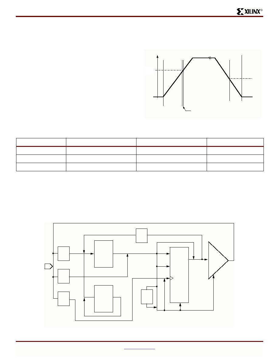
Power-Up Characteristics
CoolRunner XPLA3 CPLD I/O pins are well behaved under
all operating conditions. During power-up, CoolRunner
XPLA3 devices employ internal circuitry which keeps the
devices in the quiescent state until the V
CCINT
supply volt-
age is at a safe level (approximately 2.1V). During this time,
all I/O pins and JTAG pins are disabled, with the pins weakly
pulled high, and dedicated inputs/clocks are High-Z, as
shown in
Table 3
. When the supply voltage reaches a safe
level, all user registers become initialized, and the device is
immediately available for operation, as shown in
Figure 7
.
If the device is in the erased state (before any user pattern
is programmed), the device outputs remain disabled with a
weak pull-up. The JTAG pins are enabled to allow the device
to be programmed at any time. All devices are shipped in
the erased state from the factory.
If the device is programmed, the device inputs and outputs
take on their configured states for normal operation.
Timing Model
The XPLA3 architecture follows a timing model that allows
deterministic timing in design and redesign. The basic tim-
ing model is shown in
Figure 8
. There is a fast path (T
LOGI1
)
into the macrocell which is used if there is a single product
term. The T
LOGI2
path is used for multiple product term tim-
ing. For optimization of logic, the XPLA3 CPLD architecture
includes a Fold-back NAND path (T
LOGI3
). There is a fast
input path to each macrocell if used as an Input Register
(T
FIN
). XPLA3 also includes universal control terms (T
UDA
)
that can be used for synchronization of the macrocell regis-
ters in different function blocks. There is slew rate control
and output enable control on a per macrocell basis.
Figure 7: Device Behavior During Power Up
V
CCINT
No
Power
3.8 V
(Typ)
0V
No
Power
Quiescent
State
Quiescent
State
User Operation
Initialization of User Registers
DS012_12_062303
2.1V
1.6V
(Typ)
(Typ)
Table 3: I/O Power-Up Characteristics
Device Circuitry
Quiescent State
Erased Device Operation
Valid User Operation
Device I/Os
Disabled with Weak Pull-up
Disabled with Weak Pull-up
As Configured
Device Inputs/Clocks
High-Z
High-Z
High-Z
JTAG Controller
Disabled with Weak Pull-up
Enabled
As Configured
Figure 8: XPLA3 Timing Model
T
IN
T
F
T
OUT
T
EN
T
SLEW
T
LOGI1,2
T
PTCK
DLT
Q
CE
S/R
T
LOGI3
T
FIN
T
GCK
T
UDA
DS017_02_031802

CoolRunner XPLA3 CPLD
DS012 (v1.7) June 23, 2003
www.xilinx.com
7
Preliminary Product Specification
1-800-255-7778
R
JTAG Testing Capability
JTAG is the commonly used acronym for the Boundary
Scan Test (BST) feature defined for integrated circuits by
IEEE Standard 1149.1. This standard defines input/output
pins, logic control functions, and commands that facilitate
both board and device level testing without the use of spe-
cialized test equipment. XPLA3 devices use the JTAG Inter-
face for In-System Programming/Reprogramming. The
JTAG command set is implemented as described in
Table 4
.
As implemented in XPLA3, the JTAG Port includes four of
the five pins (refer to
Table 5
) described in the JTAG specifi-
cation: TCK, TMS, TDI, and TDO. The fifth signal defined by
the JTAG specification is TRST (Test Reset). TRST is con-
sidered an optional signal, since it is not actually required to
perform BST or ISP. The XPLA3 saves an I/O pin for general
purpose use by not implementing the optional TRST signal
in the JTAG interface. Instead, the XPLA3 supports the test
reset functionality through the use of its power-up reset cir-
cuit.
Port Enable Pin
The Port Enable pin is used to reclaim TMS, TDO, TDI, and
TCK for JTAG ISP programming if the user has defined
these pins as general purpose I/O during device program-
ming. For ease of use, XPLA3 devices are shipped with the
JTAG port pins enabled. Please note that the Port Enable
pin must be low logic level during the power-up sequence
for the device to operate properly.
During device programming, the JTAG ISP pins can be left
as is or reconfigured as user specific I/O pins. If the JTAG
ISP pins have been used for I/O pins, simply applying high
logic level to the Port Enable pin converts the JTAG ISP pins
back to their respective programming function and the
device can be reprogrammed via ISP. After completing the
desired JTAG ISP programming function, simply return Port
Enable to Ground. This will re-establish the JTAG ISP pins
to their respective I/O function. Note that reconfiguring the
JTAG port pins as I/Os makes these pins non-JTAG ISP
functional until reclaimed by port enable. If the JTAG pins
are not required as I/O, port enable should be permanently
tied to GND. Pins associated with the JTAG port have inter-
nal weak pull ups enabled to terminate the pins. However,
in noisy environments, external 10K pull ups are recom-
mended.
The XPLA3 family allows the macrocells associated with
these pins to be used as buried logic when the JTAG/ISP
function is enabled.
Table 4: XPLA3 Low-level JTAG Boundary-scan Commands
Instruction
(Instruction
Code)
Register Used
Description
Sample/Preload
(00010)
Boundary-scan
Register
The mandatory Sample/Preload instruction allows a snapshot of the normal operation of the
component to be taken and examined. It also allows data values to be loaded into the latched parallel
outputs of the Boundary-scan Shift Register prior to selection of the other boundary-scan test
instructions.
Extest
(00000)
Boundary-scan
Register
The mandatory Extest instruction allows testing of off-chip circuitry and board level interconnections.
Data would typically be loaded onto the latched parallel outputs of Boundary-scan Shift Register
using the Sample/Preload instruction prior to selection of the Extest instruction.
Bypass
(11111)
Bypass Register
Places the 1-bit bypass register between the TDI and TDO pins, which allows the BST data to pass
synchronously through the selected device to adjacent devices during normal device operation. The
Bypass instruction can be entered by holding TDI at a constant high value and completing an
Instruction-scan cycle.
Idcode
(00001)
Boundary-scan
Register
Selects the Idcode register and places it between TDI and TDO, allowing the Idcode to be serially
shifted out of TDO. The Idcode instruction permits blind interrogation of the components assembled
onto a printed circuit board. Thus, in circumstances where the component population may vary, it is
possible to determine what components exist in a product.
High-Z
(00101)
Bypass Register
The High-Z instruction places the component in a state which all of its system logic outputs are placed
in an inactive drive state (e.g., high impedance). In this state, an in-circuit test system may drive
signals onto the connections normally driven by a component output without incurring the risk of
damage to the component. The High-Z instruction also forces the Bypass Register between TDI and
TDO
Intest
(00011)
Boundary-scan
Register
The Intest instruction selects the boundary scan register preparatory to applying tests to the logic
core of the device. This permits testing of on-chip system logic while the component is already on the
board

CoolRunner XPLA3 CPLD
8
www.xilinx.com
DS012 (v1.7) June 23, 2003
1-800-255-7778
Preliminary Product Specification
R
3V, In-System Programming (ISP)
XPLA3 allows for 3V, in-system programming/reprogram-
ming of its EEPROM cells via a JTAG interface. An on-chip
charge pump eliminates the need for externally provided
super-voltages. This allows programming on the circuit
board using only the 3V supply required by the device for
normal operation. The ISP commands implemented in
XPLA3 are specified in
Table 6.
JTAG and ISP Interfacing
A number of industry-established methods exist for
JTAG/ISP interfacing with CPLDs and other integrated cir-
cuits. The XPLA3 family supports the following methods:
∑
Xilinx HW 130
∑
PC Parallel Port
∑
Workstation or PC Serial Port
∑
Embedded Processor
∑
Automated Test Equipment
∑
Third Party Programmers
∑
Xilinx ISP Programming Tools
Table 5: JTAG Pin Description
Pin
Name
Description
TCK
Test Clock Input
Clock pin to shift the serial data and instructions in and out of the TDI and TDO pins,
respectively.
TMS
Test Mode Select
Serial input pin selects the JTAG instruction mode. TMS should be driven high during
user mode operation.
TDI
Test Data Input
Serial input pin for instructions and test data. Data is shifted in on the rising edge of
TCK.
TDO
Test Data Output
Serial output pin for instructions and test data. Data is shifted out on the falling edge
of TCK. The signal is 3-stated if data is not being shifted out of the device.
Table 6: Low-level ISP Commands
Instruction
(Register Used)
Instruction
Code
Description
Enable
(ISP Shift Register)
01001
Enables the Erase, Program, and Verify commands. Using the Enable instruction
before the Erase, Program, and Verify instructions allows the user to specify the
outputs of the device using the JTAG Boundary-Scan Sample/Preload command.
Erase
(ISP Shift Register)
01010
Erases the entire EEPROM array. User can define the outputs during this
operation by using the JTAG Sample/Preload command.
Program
(ISP Shift Register)
01011
Programs the data in the ISP Shift Register into the addressed EEPROM row. The
outputs can be defined by using the JTAG Sample/Preload command.
Disable
(ISP Shift Register)
10000
Disable instruction allows the user to leave ISP mode. It selects the ISP register
to be directly connected between TDO and TDI.
Verify
(ISP Shift Register)
01100
Transfers the data from the addressed row to the ISP Shift Register. The data can
then be shifted out and compared with the JEDEC file. The user can define the
outputs during this operation.

CoolRunner XPLA3 CPLD
DS012 (v1.7) June 23, 2003
www.xilinx.com
9
Preliminary Product Specification
1-800-255-7778
R
Absolute Maximum Ratings
(1)
Table 7: Programming Specifications
Symbol
Parameter
Min.
Max.
Unit
DC Parameters
V
CCP
V
CC
supply program/verify
3.0
3.6
V
I
CCP
I
CC
limit program/verify
(1)
-
30
mA
V
IH
Input voltage (High)
2.0
-
V
V
IL
Input voltage (Low)
-
0.8
V
V
OL
Output voltage (Low)
-
0.4
V
V
OH
Output voltage (High)
2.4
-
V
AC Parameters
F
MAX
TCK maximum frequency
-
10
MHz
P
WE
Pulse width erase
100
-
ms
P
WP
Pulse width program
10
-
ms
P
WV
Pulse width verify
10
-
µ
s
T
INIT
Initialization time
(1)
-
200
µ
s
T
MS_SU
TMS setup time before TCK
10
-
ns
T
DI_SU
TDI setup time before TCK
10
-
ns
T
MS_H
TMS hold time after TCK
20
-
ns
T
DI_H
TDI hold time after TCK
20
-
ns
T
DO_CO
TDO valid after TCK
-
30
ns
Notes:
1.
Family specification. See individual device data sheets for specific device measurements.
Symbol
Parameter
Min.
Max.
Unit
V
CC
Supply voltage
(2)
relative to GND
≠0.5
4.0
V
V
I
Input voltage
(3)
relative to GND
≠0.5
5.5
(4)
V
I
OUT
Output current, per pin
≠100
100
mA
T
J
Maximum junction temperature
≠40
150
∞
C
T
STR
Storage temperature
≠65
150
∞
C
Notes:
1.
Stresses above those listed may cause malfunction or permanent damage to the device. This is a stress rating only. Functional
operation at these or any other condition above those indicated in the operational and programming specification is not implied.
2.
The chip supply voltage must rise monotonically.
3.
Maximum DC undershoot below GND must be limited to either 0.5V or 10 mA, whichever is easier to achieve. During transitions, the
device pins may undershoot to ≠2.0V or overshoot to 7.0V, provided this over- or undershoot lasts less than 10 ns and with the
forcing current being limited to 200 mA.
4.
External I/O voltage may not exceed V
CC
by 4.0V.

CoolRunner XPLA3 CPLD
10
www.xilinx.com
DS012 (v1.7) June 23, 2003
1-800-255-7778
Preliminary Product Specification
R
Recommended Operation Conditions
Quality and Reliability Characteristics
Revision History
The following table shows the revision history for this document.
Symbol
Parameter
Test Conditions
Min.
Max.
Unit
V
CC
Supply voltage
Commercial T
A
= 0∞C to 70∞C
3.0
3.6
V
Industrial T
A
= ≠40∞C to +85∞C
2.7
3.6
V
V
IL
Low-level input voltage
0
0.8
V
V
IH
High-level input voltage
2.0
5.5
V
V
O
Output voltage
0
V
CC
V
T
R
Input rise time
-
20
ns
T
F
Input fall time
-
20
ns
Symbol
Parameter
Min
Max
Units
T
DR
Data retention
20
-
Years
N
PE
Program/erase cycles (Endurance) MOSIV devices
1,000
-
Cycles
N
PE
Program/erase cycles (Endurance) UMC devices
10,000
-
Cycles
V
ESD
Electrostatic Discharge (ESD)
2,000
-
Volts
Date
Version
Revision
02/20/00
1.0
Initial Xilinx release.
03/06/00
1.1
Minor updates.
11/30/00
1.2
Updated Macrocell numbering, I/O pins, and available packages.
02/09/01
1.3
Updated specification.
04/11/01
1.4
Under Features, changed Global 3-state to Universal 3-state. Added XCR3512XL device;
changed T
SU
numbers, added 324-pin Fineline BGA package, Programming Specs:
changed T
INIT
from 50 min. to 50 max., Quality & Rel. specs: added N
PE
for UMC
devices--10,000 cycles.
01/07/02
1.5
Table 7
: Added Note 1, changed T
INIT
from 50 to 200 (max). Changed I
CCP
from 20 to 30
(max); updated Device Family
Table 1
usable gate counts. Updated Device Family
Table 2
package types, updated I/O cell section.
Absolute Maximum Ratings
table: Changed max
supply voltage relative to GND to 4.0V to match XC9500XL and UMC standard specs.
01/06/03
1.6
Added T
PTCK
parameter to timing model. Changed F
SYSTEM
for all devices in
Table 1
.
Changed from Advance Information to Preliminary. Added Note 1 to
Figure 2
regarding
XCR3384XL TQ144 JTAG pins.
06/23/03
1.7
Added
Power-Up Characteristics
.