 | –≠–ª–µ–∫—Ç—Ä–æ–Ω–Ω—ã–π –∫–æ–º–ø–æ–Ω–µ–Ω—Ç: DS022-1 | –°–∫–∞—á–∞—Ç—å:  PDF PDF  ZIP ZIP |
© 2001 Xilinx, Inc. All rights reserved. All Xilinx trademarks, registered trademarks, patents, and disclaimers are as listed at
http://www.xilinx.com/legal.htm
.
All other trademarks and registered trademarks are the property of their respective owners. All specifications are subject to change without notice.
DS022-1 (v2.2) November 9, 2001
www.xilinx.com
Module 1 of 4
Preliminary Product Specification
1-800-255-7778
1
Features
∑
Fast, High-Density 1.8 V FPGA Family
-
Densities from 58 k to 4 M system gates
-
130 MHz internal performance (four LUT levels)
-
Designed for low-power operation
-
PCI compliant 3.3 V, 32/64-bit, 33/ 66-MHz
∑
Highly Flexible SelectI/O+TM Technology
-
Supports 20 high-performance interface standards
-
Up to 804 singled-ended I/Os or 344 differential I/O
pairs for an aggregate bandwidth of > 100 Gb/s
∑
Differential Signalling Support
-
LVDS (622 Mb/s), BLVDS (Bus LVDS), LVPECL
-
Differential I/O signals can be input, output, or I/O
-
Compatible with standard differential devices
-
LVPECL and LVDS clock inputs for 300+ MHz
clocks
∑
Proprietary High-Performance SelectLinkTM
Technology
-
Double Data Rate (DDR) to Virtex-E link
-
Web-based HDL generation methodology
∑
Sophisticated SelectRAM+TM Memory Hierarchy
-
1 Mb of internal configurable distributed RAM
-
Up to 832 Kb of synchronous internal block RAM
-
True Dual-PortTM BlockRAM capability
-
Memory bandwidth up to 1.66 Tb/s (equivalent
bandwidth of over 100 RAMBUS channels)
-
Designed for high-performance Interfaces to
External Memories
-
200 MHz ZBT* SRAMs
-
200 Mb/s DDR SDRAMs
-
Supported by free Synthesizable reference design
∑
High-Performance Built-In Clock Management Circuitry
-
Eight fully digital Delay-Locked Loops (DLLs)
-
Digitally-Synthesized 50% duty cycle for Double
Data Rate (DDR) Applications
-
Clock Multiply and Divide
-
Zero-delay conversion of high-speed LVPECL/LVDS
clocks to any I/O standard
∑
Flexible Architecture Balances Speed and Density
-
Dedicated carry logic for high-speed arithmetic
-
Dedicated multiplier support
-
Cascade chain for wide-input function
-
Abundant registers/latches with clock enable, and
dual synchronous/asynchronous set and reset
-
Internal 3-state bussing
-
IEEE 1149.1 boundary-scan logic
-
Die-temperature sensor diode
∑
Supported by Xilinx FoundationTM and Alliance SeriesTM
Development Systems
-
Further compile time reduction of 50%
-
Internet Team Design (ITD) tool ideal for
million-plus gate density designs
-
Wide selection of PC and workstation platforms
∑
SRAM-Based In-System Configuration
-
Unlimited re-programmability
∑
Advanced Packaging Options
-
0.8 mm Chip-scale
-
1.0 mm BGA
-
1.27 mm BGA
-
HQ/PQ
∑
0.18
m
m 6-Layer Metal Process
∑
100% Factory Tested
* ZBT is a trademark of Integrated Device Technology, Inc.
0
VirtexTM-E 1.8 V
Field Programmable Gate Arrays
DS022-1 (v2.2) November 9, 2001
0
0
Preliminary Product Specification
R

VirtexTM-E 1.8 V Field Programmable Gate Arrays
R
Module 1 of 4
www.xilinx.com
DS022-1 (v2.2) November 9, 2001
2
1-800-255-7778
Preliminary Product Specification
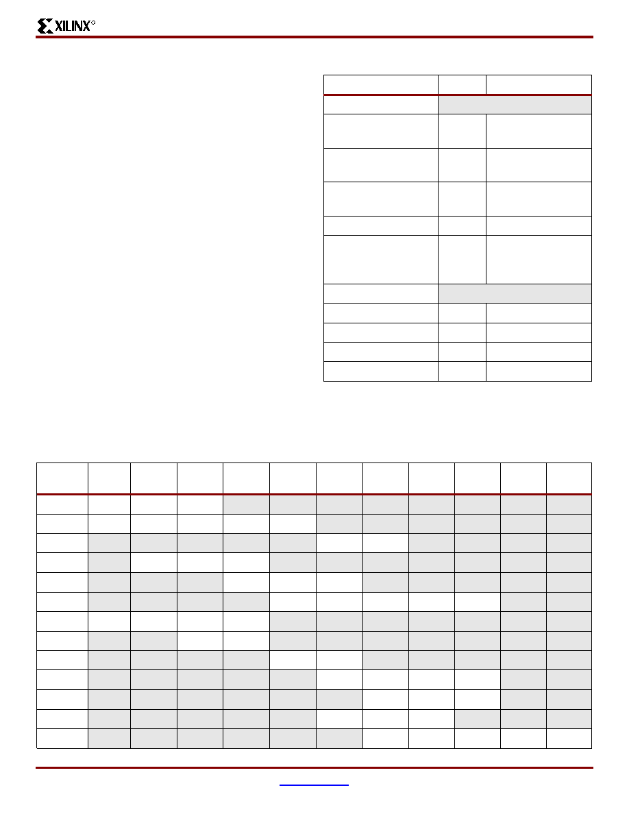
Virtex-E Compared to Virtex Devices
The Virtex-E family offers up to 43,200 logic cells in devices
up to 30% faster than the Virtex family.
I/O performance is increased to 622 Mb/s using Source
Synchronous data transmission architectures and synchro-
nous system performance up to 240 MHz using sin-
gled-ended SelectI/O technology. Additional I/O standards
are supported, notably LVPECL, LVDS, and BLVDS, which
use two pins per signal. Almost all signal pins can be used
for these new standards.
Virtex-E devices have up to 640 Kb of faster (250 MHz)
block SelectRAM, but the individual RAMs are the same
size and structure as in the Virtex family. They also have
eight DLLs instead of the four in Virtex devices. Each indi-
vidual DLL is slightly improved with easier clock mirroring
and 4x frequency multiplication.
V
CCINT
, the supply voltage for the internal logic and mem-
ory, is 1.8 V, instead of 2.5 V for Virtex devices. Advanced
processing and 0.18
m
m design rules have resulted in
smaller dice, faster speed, and lower power consumption.
I/O pins are 3 V tolerant, and can be 5 V tolerant with an
external 100
W
resistor. PCI 5 V is not supported. With the
addition of appropriate external resistors, any pin can toler-
ate any voltage desired.
Banking rules are different. With Virtex devices, all input
buffers are powered by V
CCINT
. With Virtex-E devices, the
LVTTL, LVCMOS2, and PCI input buffers are powered by
the I/O supply voltage V
CCO
.
The Virtex-E family is not bitstream-compatible with the Vir-
tex family, but Virtex designs can be compiled into equiva-
lent Virtex-E devices.
The same device in the same package for the Virtex-E and
Virtex families are pin-compatible with some minor excep-
tions. See the data sheet pinout section for details.
General Description
The Virtex-E FPGA family delivers high-performance,
high-capacity programmable logic solutions. Dramatic
increases in silicon efficiency result from optimizing the new
architecture for place-and-route efficiency and exploiting an
aggressive 6-layer metal 0.18
m
m CMOS process. These
advances make Virtex-E FPGAs powerful and flexible alter-
natives to mask-programmed gate arrays. The Virtex-E fam-
ily includes the nine members in
Table 1
.
Building on experience gained from Virtex FPGAs, the
Virtex-E family is an evolutionary step forward in program-
mable logic design. Combining a wide variety of program-
mable system features, a rich hierarchy of fast, flexible
interconnect resources, and advanced process technology,
the Virtex-E family delivers a high-speed and high-capacity
programmable logic solution that enhances design flexibility
while reducing time-to-market.
Virtex-E Architecture
Virtex-E devices feature a flexible, regular architecture that
comprises an array of configurable logic blocks (CLBs) sur-
rounded by programmable input/output blocks (IOBs), all
interconnected by a rich hierarchy of fast, versatile routing
Table 1:
Virtex-E Field-Programmable Gate Array Family Members
Device
System
Gates
Logic
Gates
CLB
Array
Logic
Cells
Differential
I/O Pairs
User
I/O
BlockRAM
Bits
Distributed
RAM Bits
XCV50E
71,693
20,736
16 x 24
1,728
83
176
65,536
24,576
XCV100E
128,236
32,400
20 x 30
2,700
83
196
81,920
38,400
XCV200E
306,393
63,504
28 x 42
5,292
119
284
114,688
75,264
XCV300E
411,955
82,944
32 x 48
6,912
137
316
131,072
98,304
XCV400E
569,952
129,600
40 x 60
10,800
183
404
163,840
153,600
XCV600E
985,882
186,624
48 x 72
15,552
247
512
294,912
221,184
XCV1000E
1,569,178
331,776
64 x 96
27,648
281
660
393,216
393,216
XCV1600E
2,188,742
419,904
72 x 108
34,992
344
724
589,824
497,664
XCV2000E
2,541,952
518,400
80 x 120
43,200
344
804
655,360
614,400
XCV2600E
3,263,755
685,584
92 x 138
57,132
344
804
753,664
812,544
XCV3200E
4,074,387
876,096
104 x 156
73,008
344
804
851,968
1,038,336
VirtexTM-E 1.8 V Field Programmable Gate Arrays
R
DS022-1 (v2.2) November 9, 2001
www.xilinx.com
Module 1 of 4
Preliminary Product Specification
1-800-255-7778
3
resources. The abundance of routing resources permits the
Virtex-E family to accommodate even the largest and most
complex designs.
Virtex-E FPGAs are SRAM-based, and are customized by
loading configuration data into internal memory cells. Con-
figuration data can be read from an external SPROM (mas-
ter serial mode), or can be written into the FPGA
(SelectMAPTM, slave serial, and JTAG modes).
The standard Xilinx Foundation SeriesTM and Alliance
SeriesTM Development systems deliver complete design
support for Virtex-E, covering every aspect from behavioral
and schematic entry, through simulation, automatic design
translation and implementation, to the creation and down-
loading of a configuration bit stream.
Higher Performance
Virtex-E devices provide better performance than previous
generations of FPGAs. Designs can achieve synchronous
system clock rates up to 240 MHz including I/O or 622 Mb/s
using Source Synchronous data transmission architech-
tures. Virtex-E I/Os comply fully with 3.3 V PCI specifica-
tions, and interfaces can be implemented that operate at
33 MHz or 66 MHz.
While performance is design-dependent, many designs
operate internally at speeds in excess of 133 MHz and can
achieve over 311 MHz.
Table 2
shows performance data for
representative circuits, using worst-case timing parameters.
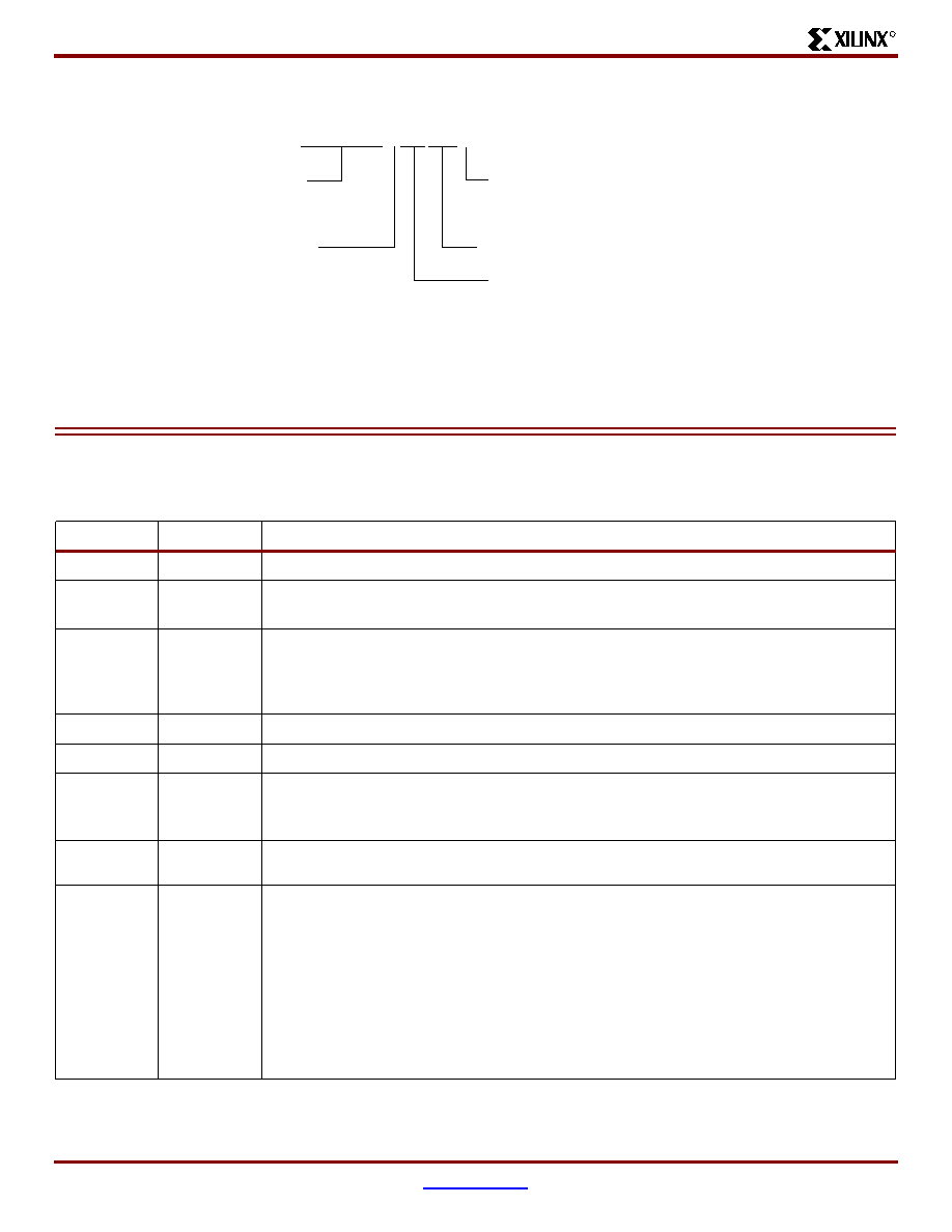
Virtex-E Device/Package Combinations and Maximum I/O
Table 2:
Performance for Common Circuit Functions
Function
Bits
Virtex-E (-7)
Register-to-Register
Adder
16
64
4.3 ns
6.3 ns
Pipelined Multiplier
8 x 8
16 x 16
4.4 ns
5.1 ns
Address Decoder
16
64
3.8 ns
5.5 ns
16:1 Multiplexer
4.6 ns
Parity Tree
9
18
36
3.5 ns
4.3 ns
5.9 ns
Chip-to-Chip
HSTL Class IV
LVTTL,16mA, fast slew
LVDS
LVPECL
Table 3:
Virtex-E Family Maximum User I/O by Device/Package (Excluding Dedicated Clock Pins)
XCV
50E
XCV
100E
XCV
200E
XCV
300E
XCV
400E
XCV
600E
XCV
1000E
XCV
1600E
XCV
2000E
XCV
2600E
XCV
3200E
CS144
94
94
94
PQ240
158
158
158
158
158
HQ240
158
158
BG352
196
260
260
BG432
316
316
316
BG560
404
404
404
404
404
FG256
176
176
176
176
FG456
284
312
FG676
404
444
FG680
512
512
512
512
FG860
660
660
660
FG900
512
660
700
FG1156
660
724
804
804
804
VirtexTM-E 1.8 V Field Programmable Gate Arrays
R
Module 1 of 4
www.xilinx.com
DS022-1 (v2.2) November 9, 2001
4
1-800-255-7778
Preliminary Product Specification
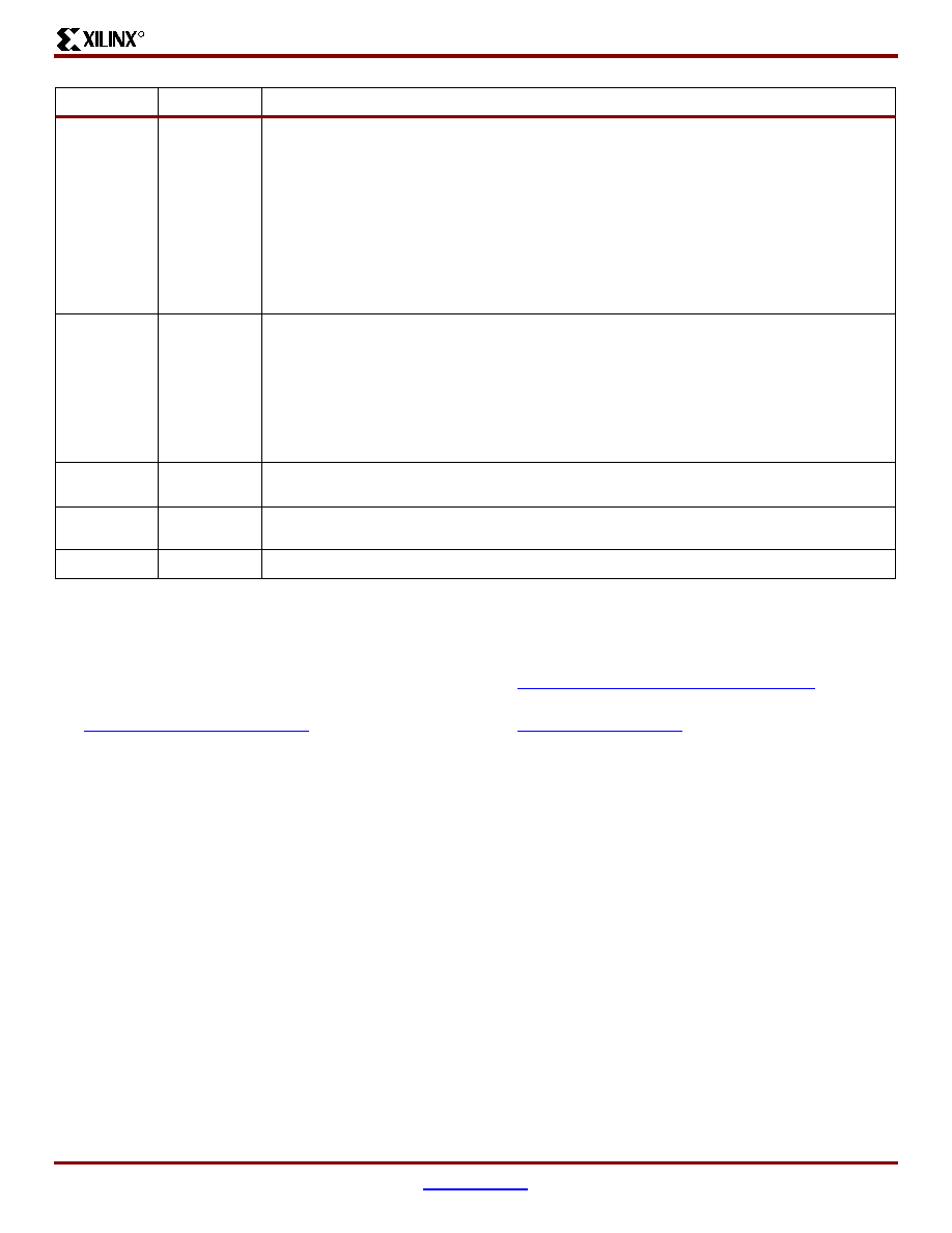
Virtex-E Ordering Information
Revision History
The following table shows the revision history for this document.
Figure 1:
Ordering Information
Date
Version
Revision
12/7/99
1.0
Initial Xilinx release.
1/10/00
1.1
Re-released with spd.txt v. 1.18, FG860/900/1156 package information, and additional DLL,
Select RAM and SelectI/O information.
1/28/00
1.2
Added Delay Measurement Methodology table, updated SelectI/O section, Figures 30, 54,
& 55, text explaining Table 5, T
BYP
values, buffered Hex Line info, p. 8, I/O Timing
Measurement notes, notes for Tables 15, 16, and corrected F1156 pinout table footnote
references.
2/29/00
1.3
Updated pinout tables, V
CC
page 20, and corrected Figure 20.
5/23/00
1.4
Correction to table on p. 22.
7/10/00
1.5
∑
Numerous minor edits.
∑
Data sheet upgraded to Preliminary.
∑
Preview -8 numbers added to Virtex-E Electrical Characteristics tables.
8/1/00
1.6
∑
Reformatted entire document to follow new style guidelines.
∑
Changed speed grade values in tables on pages 35-37.
9/20/00
1.7
∑
Min values added to Virtex-E Electrical Characteristics tables.
∑
XCV2600E and XCV3200E numbers added to Virtex-E Electrical Characteristics
tables (Module 3).
∑
Corrected user I/O count for XCV100E device in Table 1 (Module 1).
∑
Changed several pins to "No Connect in the XCV100E" and removed duplicate V
CCINT
pins in Table ~ (Module 4).
∑
Changed pin J10 to "No connect in XCV600E" in Table 74 (Module 4).
∑
Changed pin J30 to "VREF option only in the XCV600E" in Table 74 (Module 4).
∑
Corrected pair 18 in Table 75 (Module 4) to be "AO in the XCV1000E, XCV1600E".
Example: XCV300E-6PQ240C
Device Type
Temperature Range
C = Commercial (Tj = 0 C to +85 C)
I = Industrial (Tj = -40 C to +100 C)
Number of Pins
Package Type
BG = Ball Grid Array
FG = Fine Pitch Ball Grid Array
HQ = High Heat Dissipation
Speed Grade
(-6, -7, -8)
DS022_043_072000
VirtexTM-E 1.8 V Field Programmable Gate Arrays
R
DS022-1 (v2.2) November 9, 2001
www.xilinx.com
Module 1 of 4
Preliminary Product Specification
1-800-255-7778
5
Virtex-E Data Sheet
The Virtex-E Data Sheet contains the following modules:
∑
DS022-1, Virtex-E 1.8V FPGAs:
Introduction and Ordering Information (Module 1)
∑
DS022-2, Virtex-E 1.8V FPGAs:
Functional Description (Module 2)
∑
DS022-3, Virtex-E 1.8V FPGAs:
DC and Switching Characteristics (Module 3)
∑
DS022-4, Virtex-E 1.8V FPGAs:
Pinout Tables (Module 4)
11/20/00
1.8
∑
Upgraded speed grade -8 numbers in Virtex-E Electrical Characteristics tables to
Preliminary.
∑
Updated minimums in Table 13 and added notes to Table 14.
∑
Added to note 2 to Absolute Maximum Ratings.
∑
Changed speed grade -8 numbers for T
SHCKO32
, T
REG
, T
BCCS
, and T
ICKOF
.
∑
Changed all minimum hold times to ≠0.4 under Global Clock Setup and Hold for
LVTTL Standard, with DLL.
∑
Revised maximum T
DLLPW
in -6 speed grade for DLL Timing Parameters.
∑
Changed GCLK0 to BA22 for FG860 package in Table 46.
2/12/01
1.9
∑
Revised footnote for Table 14.
∑
Added numbers to Virtex-E Electrical Characteristics tables for XCV1000E and
XCV2000E devices.
∑
Updated Table 27 and Table 78 to include values for XCV400E and XCV600E devices.
∑
Revised Table 62 to include pinout information for the XCV400E and XCV600E devices
in the BG560 package.
∑
Updated footnotes 1 and 2 for Table 76 to include XCV2600E and XCV3200E devices.
4/2/01
2.0
∑
Updated numerous values in
Virtex-E Switching Characteristics
tables.
∑
Converted data sheet to modularized format. See the
Virtex-E Data Sheet
section.
10/25/01
2.1
∑
Updated the
Virtex-E Device/Package Combinations and Maximum I/O
table to
show XCV3200E in the FG1156 package.
11/09/01
2.2
∑
Minor edits.
Date
Version
Revision