 | –≠–ª–µ–∫—Ç—Ä–æ–Ω–Ω—ã–π –∫–æ–º–ø–æ–Ω–µ–Ω—Ç: TDOXZ | –°–∫–∞—á–∞—Ç—å:  PDF PDF  ZIP ZIP |

September 17, 1999 (Version 1.3)
1
d
Features
∑
In-system programmable 3.3V PROMs for configuration
of Xilinx FPGAs
-
Endurance of 10,000 program/erase cycles
-
Program/erase over full commercial voltage and
temperature range
∑
IEEE Std 1149.1 boundary-scan (JTAG) support
∑
Simple interface to the FPGA; could be configured to
use only one user I/O pin
∑
Cascadable for storing longer or multiple bitstreams
∑
Dual configuration modes
-
Serial Slow/Fast configuration (up to 15 mHz).
-
Parallel
∑
Low-power advanced CMOS FLASH process
∑
5 V tolerant I/O pins accept 5 V, 3.3 V and 2.5 V signals.
∑
3.3 V or 2.5 V output capability
∑
Available in PC20, SO20, PC44 and VQ44 packages.
∑
Design support using the Xilinx Alliance and
Foundation series software packages.
∑
JTAG command initiation of standard FPGA
configuration.
Description
Xilinx introduces the XC1800 series of in-system program-
mable configuration PROMs. Initial devices in this 3.3V
family are a 4 megabit, a 2 megabit, a 1 megabit, a 512
Kbit, a 256 Kbit, and a 128 Kbit PROM that provide an
easy-to-use, cost-effective method for re-programming and
storing large Xilinx FPGA or CPLD configuration bit-
streams.
When the FPGA is in Master Serial mode, it generates a
configuration clock that drives the PROM. A short access
time after the rising CCLK, data is available on the PROM
DATA (D0) pin that is connected to the FPGA DIN pin. The
FPGA generates the appropriate number of clock pulses to
complete the configuration. When the FPGA is in Slave
Serial mode, the PROM and the FPGA are clocked by an
external clock.
When the FPGA is in Express or SelectMAP Mode, an
external oscillator will generate the configuration clock that
drives the PROM and the FPGA. After the rising CCLK
edge, data are available on the PROM's DATA (D0-D7)
pins. The data will be clocked into the FPGA on the follow-
ing rising edge of the CCLK. Neither Express nor Select-
MAP utilize a Length Count, so a free-running oscillator
may be used. See
Figure 5
Multiple devices can be concatenated by using the CEO
output to drive the CE input of the following device. The
clock inputs and the DATA outputs of all PROMs in this
chain are interconnected. All devices are compatible and
can be cascaded with other members of the family or with
the XC1700L one-time programmable Serial PROM family.
0
XC1800 Series of In-System
Programmable Configuration
PROMs
September 17, 1999 (Version 1.3)
0
6*
Preliminary Product Specification
Æ
Figure 1: XC1800 Series Block Diagram
Control
and
JTAG
Interface
Memory
Serial
or
Parallel
Interface
D0 DATA
(Serial or Parallel
(Express/SelectMAP)
Mode)
D1 - D7
Express Mode and
SelectMAP Interface
Data
Address
CLK
CE
TCK
TMS
TDI
TDO
OE/Reset
CEO
Data
99020300
CF
R
XC1800 Series of In-System Programmable Configuration PROMs
2
September 17, 1999 (Version 1.3)
Pinout and Pin Description
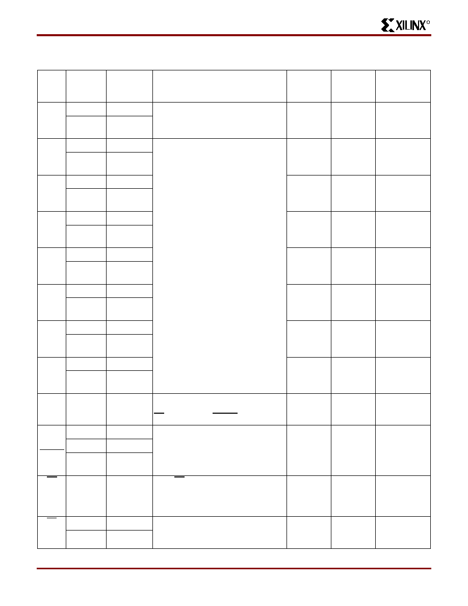
Table 1: Pin Names and Descriptions
Pin
Name
Boundary
Scan
Order
Function
Pin Description
44-pin
VQFP
44-pin
PLCC
20-pin
SOIC & PLCC
D0
4
DATA OUT D0 is the DATA output pin to provide data
for configuring an FPGA in serial mode.
40
2
1
3
OUTPUT
ENABLE
D1
6
DATA OUT D0- D7 are the output pins to provide par-
allel data for configuring a Xilinx FPGA in
express mode.
29
35
16
5
OUTPUT
ENABLE
D2
2
DATA OUT
42
4
2
1
OUTPUT
ENABLE
D3
8
DATA OUT
27
33
15
7
OUTPUT
ENABLE
D4
24
DATA OUT
9
15
7*
23
OUTPUT
ENABLE
D5
10
DATA OUT
25
31
14
9
OUTPUT
ENABLE
D6
17
DATA OUT
14
20
9
16
OUTPUT
ENABLE
D7
14
DATA OUT
19
25
12
13
OUTPUT
ENABLE
CLK
0
DATA IN
Each rising edge on the CLK input incre-
ments the internal address counter if both
CE is low and OE/RESET is high.
43
5
3
OE/
RESET
20
DATA IN
When Low, this input holds the address
counter reset and the DATA output at
high impedance.
13
19
8
19
DATA OUT
18
OUTPUT
ENABLE
CE
15
DATA IN
When CE is High, this pin puts the device
into standby mode. The DATA output pin
is at High impedance, and the device is in
low power standby mode.
15
21
10
CF
22
DATA OUT Allows JTAG CONFIG instruction to ini-
tiate FPGA configuration without power-
ing down FPGA.
10
16
7*
21
DATA IN

R
September 17, 1999 (Version 1.3)
3
XC1800 Series of In-System Programmable Configuration PROMs
*Programmable for Serial Mode only on 18512 and 1801.
CEO
13
DATA OUT Chip Enable (CEO) output is connected
to the CE input of the next PROM in the
chain. This output is Low when the CE
and OE/RESET inputs are active AND
the internal address counter has been in-
cremented beyond its Terminal Count
(TC) value. When the PROM has been
read, CEO will follow CE as long as OE/
RESET is High. When OE/RESET goes
Low, CEO stays High until the PROM is
brought out of reset by bringing OE/RE-
SET High. CEO can be programmed to
be either active High or active Low.
21
27
13
14
OUTPUT
ENABLE
GND
GND is the ground connection.
6, 18, 28 &
41
3, 12, 24 &
34
11
TMS
MODE
SELECT
The state of TMS on the rising edge of
TCK determines the state transitions at
the Test Access Port (TAP) controller.
TMS has an internal 50K ohm resistive
pull-up on it to provide a logic 1 to the de-
vice if the pin is not driven.
5
11
5
TCK
CLOCK
This pin is the JTAG test clock. It se-
quences the TAP controller and all the
JTAG test and programming electronics.
7
13
6
TDI
DATA IN
This pin is the serial input to all JTAG in-
struction and data registers. TDI has an
internal 50K ohm resistive pull-up on it to
provide a logic 1 to the system if the pin is
not driven.
3
9
4
TDO
DATA OUT This pin is the serial output for all JTAG
instruction and data registers. TDO has
an internal 50k ohm resistive pull-up on it
to provide a logic 1 to the system if the pin
is not driven.
31
37
17
V
CC
Positive voltage supply of 3.3V for inter-
nal logic and input buffers.
17, 35 & 38
23, 41 & 44
18 & 20
V
CCO
Positive voltage supply connected to the
output voltage drivers.
8, 16, 26 &
36
14, 22, 32 &
42
19
Pin
Name
Boundary
Scan
Order
Function
Pin Description
44-pin
VQFP
44-pin
PLCC
20-pin
SOIC & PLCC

R
XC1800 Series of In-System Programmable Configuration PROMs
4
September 17, 1999 (Version 1.3)
Xilinx FPGAs and Compatible
PROMs
Capacity
Device
Configuration Bits
PROM
XC4003E
53,984
XC18128
XC4005E
95,008
XC18128
XC4006E
119,840
XC18128
XC4008E
147,552
XC18256
XC4010E
178,144
XC18256
XC4013E
247,968
XC18256
XC4020E
329,312
XC18512
XC4025E
422,176
XC18512
XC4002XL
61,100
XC18128
XC4005XL
151,960
XC18256
XC4010XL
283,424
XC18512
XC4013XL/XLA
393,632
XC18512
XC4020XL/XLA
521,880
XC18512
XC4028XL/XLA
668,184
XC1801
XC4036XL/XLA
832,528
XC1801
XC4044XL/XLA
1,014,928
XC1801
XC4052XL/XLA
1,215,368
XC1802
XC4062XL/XLA
1,433,864
XC1802
XC4085XL/XLA
1,924,992
XC1802
XC40110XV
2,686,136
XC1804
XC40150XV
3,373,448
XC1804
XC40200XV
4,551,056
XC1804 +
XC18512
XC40250XV
5,433,888
XC1804 +
XC1802
XCV50
559,232
XC1801
XCV100
781,248
XC1801
XCV150
1,041,128
XC1801
XCV200
1,335,872
XC1802
XCV300
1,751,840
XC1802
XCV400
2,546,080
XC1804
XCV600
3,608,000
XC1804
XCV800
4,715,648
XC1804 +
XC18512
XCV1000
6,127,776
XC1804 +
XC1802
Devices
Configuration Bits
1804
4,194,304
1802
2,097,152
1801
1,048,576
18512
524,288
18256
262,144
18128
131,072
R
September 17, 1999 (Version 1.3)
5
XC1800 Series of In-System Programmable Configuration PROMs
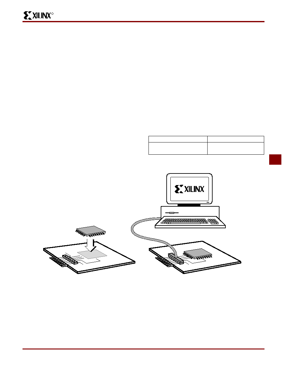
In-System Programming
One or more in-system programmable PROMs can be
daisy chained together and programmed in-system via the
standard 4-pin JTAG protocol as shown in
Figure 2
. In-sys-
tem programming offers quick and efficient design itera-
tions and eliminates unnecessary package handling or
socketing of devices. The Xilinx development system pro-
vides the programming data sequence using Xilinx JTAG
Programmer software and a download cable, a third-party
JTAG development system, a JTAG-compatible board
tester, or a simple microprocessor interface that emulates
the JTAG instruction sequence.
All outputs are 3-stated or held at clamp levels during in-
system programming.
External Programming
Xilinx reprogrammable PROMs can also be programmed
by the Xilinx HW-130 device programmer. This provides the
added flexibility of using pre-programmed devices in
design, boundary-scan manufacturing tools, with an in-sys-
tem programmable option for future enhancements and
design changes.
Reliability and Endurance
Xilinx in-system programmable products provide a mini-
mum endurance level of 10,000 in-system program/erase
cycles and a minimum data retention of 10 years. Each
device meets all functional, performance, and data reten-
tion specifications within this endurance limit.
Design Security
The Xilinx in-system programmable PROM devices incor-
porate advanced data security features to fully protect the
programming data against unauthorized reading.
Table 2
shows the security setting available.
The read security bit can be set by the user to prevent the
internal programming pattern from being read or copied via
JTAG. When set it allows device erase. Erasing the entire
device is the only way to reset the read security bit.
Table 2: Data Security Options
Default
Set
Read Allowed
Program/Erase Allowed
Read Inhibited via JTAG
Erase Allowed
X5902
GND
V
CC
(a)
(b)
Figure 2: In-System Programming Operation (a) solder device to PCB and (b) Program using Download Cable