
December 10, 1997 (Version 1.1)
5-1
Features
∑
On-chip address counter, incremented by each rising
edge on the clock input
∑
Simple interface to the FPGA; requires only one user
I/O pin
∑
Cascadable for storing longer or multiple bitstreams
∑
Programmable reset polarity (active High or active Low)
for compatibility with different FPGA solutions
∑
Supports XC4000EX/XL fast configuration mode (15.0
MHz)
∑
Low-power CMOS Floating Gate process
∑
Available in 5 V and 3.3 V versions
∑
Available in compact plastic packages: 8-pin PDIP,
20-pin SOIC, and 20-pin PLCC.
∑
Programming support by leading programmer
manufacturers.
∑
Design support using the Xilinx Alliance and
Foundation series software packages.
Description
The XC1701L, XC1701 and XC17512L serial configuration
PROMs (SCPs) provide an easy-to-use, cost-effective
method for storing Xilinx FPGA configuration bitstreams.
When the FPGA is in master serial mode, it generates a
configuration clock that drives the SCP. A short access time
after the rising clock edge, data appears on the SCP DATA
output pin that is connected to the FPGA DIN pin. The
FPGA generates the appropriate number of clock pulses to
complete the configuration. Once configured, it disables the
SCP. When the FPGA is in slave mode, the SCP and the
FPGA must both be clocked by an incoming signal.
Multiple devices can be concatenated by using the CEO
output to drive the CE input of the following device. The
clock inputs and the DATA outputs of all SCPs in this chain
are interconnected. All devices are compatible and can be
cascaded with other members of the family.
For device programming, either the Xilinx Alliance or Foun-
dation series development system compiles the FPGA
design file into a standard Hex format, which is then trans-
ferred to the programmer.
0
XC1701L
(3.3V),
XC1701
(5.0V) and
XC17512L
(3.3V)
Serial Configuration PROMs
December 10, 1997 (Version 1.1)
0
5*
Product Specification
Æ
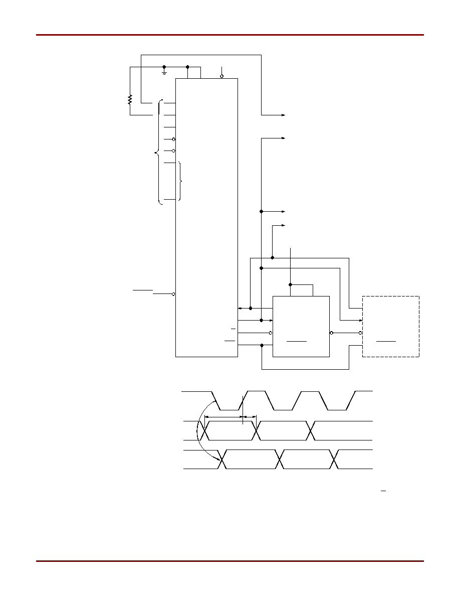
Figure 1: Simplified Block Diagram (does not show programming circuit)
EPROM
Cell
Matrix
Address Counter
CE
RESET/
OE or
OE/
RESET
DATA
CEO
OE
Output
CLK
V
CC
V
PP
GND
X3185
TC

XC1701L (3.3V), XC1701 (5.0V) and XC17512L (3.3V) Serial Configuration PROMs
5-2
December 10, 1997 (Version 1.1)
Pin Description
DATA
Data output, 3-stated when either CE or OE are inactive.
During programming, the DATA pin is I/O. Note that OE can
be programmed to be either active High or active Low.
CLK
Each rising edge on the CLK input increments the internal
address counter, if both CE and OE are active.
RESET/OE
When High, this input holds the address counter reset and
3-states the DATA output. The polarity of this input pin is
programmable as either RESET/OE or OE/RESET. To
avoid confusion, this document describes the pin as
RESET/OE, although the opposite polarity is possible on all
devices. When RESET is active, the address counter is
held at zero, and the DATA output is 3-stated. The polarity
of this input is programmable. The default is active High
RESET, but the preferred option is active Low RESET,
because it can be driven by the FPGA's INIT pin.
The polarity of this pin is controlled in the programmer inter-
face. This input pin is easily inverted using the Xilinx HW-
130 Programmer. Third-party programmers have different
methods to invert this pin.
CE
When High, this pin disables the internal address counter,
3-states the DATA output, and forces the device into low-I
CC
standby mode.
CEO
Chip Enable output, to be connected to the CE input of the
next SCP in the daisy chain. This output is Low when the
CE and OE inputs are both active AND the internal address
counter has been incremented beyond its Terminal Count
(TC) value. In other words: when the PROM has been read,
CEO will follow CE as long as OE is active. When OE goes
inactive, CEO stays High until the PROM is reset. Note that
OE can be programmed to be either active High or active
Low.
V
PP
Programming voltage. No overshoot above the specified
max voltage is permitted on this pin. For normal read oper-
ation, this pin
must be connected to V
CC
. Failure to do so
may lead to unpredictable, temperature-dependent opera-
tion and severe problems in circuit debugging.
Do not leave
VPP floating!
V
CC
and GND
Positive supply and ground pins.
Serial PROM Pinouts
Capacity
Number of Configuration Bits, Including
Header for all Xilinx FPGAs and Compatible
SCP Type
Pin Name
8-Pin
PDIP
20-Pin
SOIC
20-Pin
PLCC
DATA
1
1
2
CLK
2
3
4
RESET/OE (OE/RESET)
3
8
6
CE
4
10
8
GND
5
11
10
CEO
6
13
14
V
PP
7
18
17
V
CC
8
20
20
Device
Configuration Bits
XC1701L
1,048,576
XC1701
1,048,576
XC17512L
524,288
Device
Configuration Bits
SPROM
XC4010XL
283,424
XC17512L
XC4013XL
393,623
XC17512L
XC4020E
329,312
XC1701
XC4020XL
521,880
XC17512L
XC4025E
422,176
XC1701
XC4028XL
668,184
XC1701L
XC4028EX
668,184
XC1701
XC4036EX
832,528
XC1701
XC4036XL
832,528
XC1701L
XC4044XL
1,014,928
XC1701L
XC4052XL
1,215,368
XC1701L +
XC17256L
XC4062XL
1,433,864
XC1701L +
XC17512L
XC4085XL
1,924,992
2 x XC1701L

December 10, 1997 (Version 1.1)
5-3
Controlling Serial PROMs
Most connections between the FPGA device and the Serial
PROM are simple and self-explanatory.
∑
The DATA output(s) of the of the Serial PROM(s) drives
the DIN input of the lead FPGA device.
∑
The master FPGA CCLK output drives the CLK input(s)
of the Serial PROM(s).
∑
The CEO output of a Serial PROM drives the CE input
of the next Serial PROM in a daisy chain (if any).
∑
The RESET/OE input of all Serial PROMs is best driven
by the INIT output of the XC3000 or XC4000 lead
FPGA device. This connection assures that the Serial
PROM address counter is reset before the start of any
(re)configuration, even when a reconfiguration is
initiated by a V
CC
glitch. Other methods ≠ such as
driving RESET/OE from LDC or system reset ≠ assume
that the Serial PROM internal power-on-reset is always
in step with the FPGA's internal power-on-reset, which
may not be a safe assumption.
∑
The CE input of the lead (or only) Serial PROM is driven
by the DONE/PRGM or DONE output of the lead FPGA
device, provided that DONE/PRGM is not permanently
grounded. Otherwise, LDC can be used to drive CE, but
must then be unconditionally High during user
operation. CE can also be permanently tied Low, but
this keeps the DATA output active and causes an
unnecessary supply current of 10 mA maximum.
FPGA Master Serial Mode Summary
The I/O and logic functions of the Logic Cell Array and their
associated interconnections are established by a configu-
ration program. The program is loaded either automatically
upon power up, or on command, depending on the state of
the three FPGA mode pins. In Master Mode, the FPGA
automatically loads the configuration program from an
external memory. The Serial Configuration PROM has
been designed for compatibility with the Master Serial
Mode.
Upon power-up or reconfiguration, an FPGA enters the
Master Serial Mode whenever all three of the FPGA mode-
select pins are Low (M0=0, M1=0, M2=0). Data is read from
the Serial Configuration PROM sequentially on a single
data line. Synchronization is provided by the rising edge of
the temporary signal CCLK, which is generated during con-
figuration.
Master Serial Mode provides a simple configuration inter-
face. Only a serial data line and two control lines are
required to configure an FPGA. Data from the Serial Con-
figuration PROM is read sequentially, accessed via the
internal address and bit counters which are incremented on
every valid rising edge of CCLK.
If the user-programmable, dual-function DIN pin on the
FPGA is used only for configuration, it must still be held at
a defined level during normal operation. The XC3000 and
XC4000 families take care of this automatically with an on-
chip default pull-up resistor.
Programming the FPGA With Counters
Unchanged Upon Completion
When multiple FPGA-configurations for a single FPGA are
stored in a Serial Configuration PROM, the OE pin should
be tied Low. Upon power-up, the internal address counters
are reset and configuration begins with the first program
stored in memory. Since the OE pin is held Low, the
address counters are left unchanged after configuration is
complete. Therefore, to reprogram the FPGA with another
program, the D/P line is pulled Low and configuration
begins at the last value of the address counters.
This method fails if a user applies RESET during the FPGA
configuration process. The FPGA aborts the configuration
and then restarts a new configuration, as intended, but the
Serial PROM does not reset its address counter, since it
never saw a High level on its OE input. The new configura-
tion, therefore, reads the remaining data in the PROM and
interprets it as preamble, length count etc. Since the FPGA
is the master, it issues the necessary number of CCLK
pulses, up to 16 million (24) and D/P goes High. However,
the FPGA configuration will be completely wrong, with
potential contentions inside the FPGA and on its output
pins. This method must, therefore, never be used when
there is any chance of external reset during configuration.
Cascading Serial Configuration PROMs
For multiple FPGAs configured as a daisy-chain, or for
future FPGAs requiring larger configuration memories, cas-
caded SCPs provide additional memory. After the last bit
from the first SCP is read, the next clock signal to the SCP
asserts its CEO output Low and disables its DATA line. The
second SCP recognizes the Low level on its CE input and
enables its DATA output. See
Figure 2
.
After configuration is complete, the address counters of all
cascaded SCPs are reset if the FPGA RESET pin goes
Low, assuming the SCP reset polarity option has been
inverted.
To reprogram the FPGA with another program, the D/P line
goes Low and configuration begins where the address
counters had stopped. In this case, avoid contention
between DATA and the configured I/O use of DIN.
XC1701L (3.3V), XC1701 (5.0V) and XC17512L (3.3V) Serial Configuration PROMs
5-4
December 10, 1997 (Version 1.1)
Figure 2: Master Serial Mode. The one-time-programmable Serial Configuration PROM supports automatic loading of
configuration programs. Multiple devices can be cascaded to support additional FPGA. An early D/P inhibits the
PROM data output one CCLK cycle before the FPGA I/Os become active.
* If Readback is
Activated, a
3.3-k
Resistor is
Required in
Series With M1
During Configuration
the 3.3 k
M2 Pull-Down
Resistor Overcomes the
Internal Pull-Up,
but it Allows M2 to
be User I/O.
General-
Purpose
User I/O
Pins
Other
I/O Pins
M2
HDC
LDC
INIT
RESET
DIN
CCLK
INIT
D/P
SCP
DATA
CEO
CLK
CE
OPTIONAL
Slave FPGAs
with Identical
Configurations
Vcc
*
M0 M1 PWRDWN
FPGA
(Low Resets the Address Pointer)
∑
∑
∑
∑
∑
Vcc
VCC
VPP
RESET
X8256
Cascaded
Serial
Memory
DATA
CLK
CE
OPTIONAL
Daisy-chained
FPGAs with
Different
Configurations
DOUT
CCLK
(OUTPUT)
DIN
DOUT
(OUTPUT)
OE/RESET
OE/RESET

December 10, 1997 (Version 1.1)
5-5
Standby Mode
The PROM enters a low-power standby mode whenever
CE is asserted High. The output remains in a high imped-
ance state regardless of the state of the OE input.
Programming
The devices can be programmed on programmers supplied
by Xilinx or qualified third-party vendors. The user must
ensure that the appropriate programming algorithm and the
latest version of the programmer software are used. The
wrong choice can permanently damage the device.
Notes:
1.
The XC1700 RESET input has programmable polarity
2.
TC = Terminal Count = highest address value. TC+1 = address 0.
IMPORTANT: Always tie the V
PP
pin to V
CC
in your application. Never leave V
PP
floating.
Table 1: Truth Table for XC1700 Control Inputs
Control Inputs
Internal Address
Outputs
RESET
CE
DATA
CEO
I
cc
Inactive
Low
if address < TC: increment
if address > TC: don't change
active
3-state
High
Low
active
reduced
Active
Low
Held reset
3-state
High
active
Inactive
High
Not changing
3-state
High
standby
Active
High
Held reset
3-state
High
standby

XC1701L (3.3V), XC1701 (5.0V) and XC17512L (3.3V) Serial Configuration PROMs
5-6
December 10, 1997 (Version 1.1)
XC1701
Absolute Maximum Ratings
Note:
Stresses beyond those listed under Absolute Maximum Ratings may cause permanent damage to the device. These are
stress ratings only, and functional operation of the device at these or any other conditions beyond those listed under
Operating Conditions is not implied. Exposure to Absolute Maximum Ratings conditions for extended periods of time may
affect device reliability.
Operating Conditions
DC Characteristics Over Operating Condition
Note
: During normal read operation V
PP
must be connected to V
CC
Symbol
Description
Units
V
CC
Supply voltage relative to GND
-0.5 to +7.0
V
V
PP
Supply voltage relative to GND
-0.5 to +12.5
V
V
IN
Input voltage relative to GND
-0.5 to V
CC
+0.5
V
V
TS
Voltage applied to 3-state output
-0.5 to V
CC
+0.5
V
T
STG
Storage temperature (ambient)
-65 to +150
∞
C
T
SOL
Maximum soldering temperature (10 s @ 1/16 in.)
+260
∞
C
Symbol
Description
Min
Max
Units
V
CC
Commercial
Supply voltage relative to GND 0
∞
C to +70
∞
C junction
4.75
5.25
V
Industrial
Supply voltage relative to GND -40
∞
C to +85
∞
C junction
4.50
5.50
V
Military
Supply voltage relative to GND -55
∞
C to +125
∞
C case
4.50
5.50
V
Symbol
Description
Min
Max
Units
V
IH
High-level input voltage
2.0
V
CC
V
V
IL
Low-level input voltage
0
0.8
V
V
OH
High-level output voltage (I
OH
= -4 mA)
Commercial
3.86
V
V
OL
Low-level output voltage (I
OL
= +4 mA)
0.32
V
V
OH
High-level output voltage (I
OH
= -4 mA)
Industrial
3.76
V
V
OL
Low-level output voltage (I
OL
= +4 mA)
0.37
V
I
CCA
Supply current, active mode
10.0
mA
I
CCS
Supply current, standby mode
50.0
µ
A
I
L
Input or output leakage current
-10.0
10.0
µ
A
December 10, 1997 (Version 1.1)
5-7
XC1701L/XC17512L
Absolute Maximum Ratings
Note:
Stresses beyond those listed under Absolute Maximum Ratings may cause permanent damage to the device. These are stress
ratings only, and functional operation of the device at these or any other conditions beyond those listed under Operating
Conditions is not implied. Exposure to Absolute Maximum Ratings conditions for extended periods of time may affect device
reliability.
Operating Conditions
DC Characteristics Over Operating Condition
Note:
During normal read operation V
PP
must be connected to V
CC
Symbol
Description
Units
V
CC
Supply voltage relative to GND
-0.5 to +6.0
V
V
PP
Supply voltage relative to GND
-0.5 to +12.5
V
V
IN
Input voltage with respect to GND
-0.5 to V
CC
+0.5
V
V
TS
Voltage applied to 3-state output
-0.5 to V
CC
+0.5
V
T
STG
Storage temperature (ambient)
-65 to +150
∞
C
T
SOL
Maximum soldering temperature (10 s @ 1/16 in.)
+260
∞
C
Symbol
Description
Min
Max
Units
V
CC
Commercial
Supply voltage relative to GND 0
∞
C to +70
∞
C junction
3.0
3.6
V
Symbol
Description
Min
Max
Units
V
IH
High-level input voltage
2.0
V
CC
V
V
IL
Low-level input voltage
0
0.8
V
V
OH
High-level output voltage (I
OH
= -4 mA)
2.4
V
V
OL
Low-level output voltage (I
OL
= +4 mA)
0.4
V
I
CCA
Supply current, active mode
5.0
mA
I
CCS
Supply current, standby mode
50.0
µ
A
I
L
Input or output leakage current
-10.0
10.0
µ
A
XC1701L (3.3V), XC1701 (5.0V) and XC17512L (3.3V) Serial Configuration PROMs
5-8
December 10, 1997 (Version 1.1)
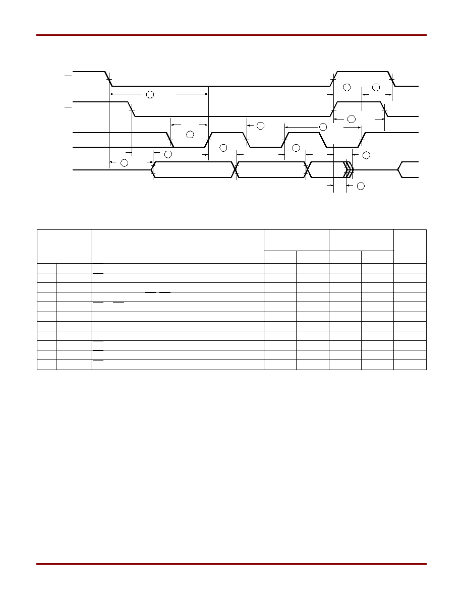
AC Characteristics Over Operating Condition
Notes:
1. AC test load = 50 pF
2. Float delays are measured with minimum tester ac load and maximum dc load.
3. Guaranteed by design, not tested.
4. All AC parameters are measured with V
IL
= 0.0 V and V
IH
= 3.0 V.
RESET/OE
CE
CLK
DATA
1
T
CE
2
T
OE
T
LC
7
9
T
SCE
T
SCE
T
HCE
T
HOE
11
T
CAC
T
OH
T
DF
5
T
OH
4
4
3
9
10
T
HC
8
X2634
T
CYC
6
Symbol
Description
XC1701
XC1701L
XC17512L
Units
Min
Max
Min
Max
1
T
OE
OE to Data Delay
25
30
ns
2
T
CE
CE to Data Delay
45
60
ns
3
T
CAC
CLK to Data Delay
45
60
ns
4
T
OH
Data Hold From CE, OE, or CLK
0
0
ns
5
T
DF
CE or OE to Data Float Delay
2
50
50
ns
6
T
CYC
Clock Periods
67
100
ns
7
T
LC
CLK Low Time
3
20
25
ns
8
THC
CLK High Time
3
20
25
ns
9
TSCE
CE Setup Time to CLK (to guarantee proper counting)
20
25
ns
10
T
HCE
CE Hold Time to CLK (to guarantee proper counting)
0
0
ns
11
T
HOE
OE Hold Time (guarantees counters are reset)
20
25
ns

December 10, 1997 (Version 1.1)
5-9
AC Characteristics Over Operating Condition (continued)
Notes:
1. AC test load = 50 pF
2. Float delays are measured with minimum tester ac load and maximum dc load.
3. Guaranteed by design, not tested.
4. All AC parameters are measured with V
IL
= 0.0 V and V
IH
= 3.0 V.
Symbol
Description
XC1701
XC1701L
XC17512L
Units
Min
Max
Min
Max
12
T
CDF
CLK to Data Float Delay
2
50
50
ns
13
T
OCK
CLK to CEO Delay
30
30
ns
14
T
OCE
CE to CEO Delay
35
35
ns
15
T
OOE
RESET/OE to CEO Delay
30
30
ns
RESET/OE
CLK
DATA
CE
15 T
OOE
CEO
First Bit
Last Bit
T
OCE
13 T
OCK
12 T
CDF
X3183
14
T
OCE
14

XC1701L (3.3V), XC1701 (5.0V) and XC17512L (3.3V) Serial Configuration PROMs
5-10 December 10, 1997 (Version 1.1)
Ordering Information
Marking Information
Due to the small size of the serial PROM package, the complete ordering part number cannot be marked on the package.
The XC prefix is deleted and the package code is simplified. Device marking is as follows.
XC1701L PC20 C
Operating Range/Processing
C = Commercial (0
∞
to +70
∞
C)
I = Industrial (≠40
∞
to +85
∞
C)
Package Type
PD8 = 8-Pin Plastic DIP
SO20 = 20-Pin Plastic Small-Outline Package
PC20 = 20-Pin Plastic Leaded Chip Carrier
Device Number
XC1701L
XC1701
XC17512L
1701L P C
Operating Range/Processing
C = Commercial (0
∞
to +70
∞
C)
I = Industrial (≠40
∞
to +85
∞
C)
Package Type
P = 8-Pin Plastic DIP
S = 20-Pin Plastic Small-Outline Package
J = 20-Pin Plastic Leaded Chip Carrier
Device Number
XC1701L
XC1701
XC17512L