
DS060 (v1.6) September 19, 2001
www.xilinx.com
1
Product Specification
1-800-255-7778
� 2001 Xilinx, Inc. All rights reserved. All Xilinx trademarks, registered trademarks, patents, and disclaimers are as listed at
http://www.xilinx.com/legal.htm
.
All other trademarks and registered trademarks are the property of their respective owners. All specifications are subject to change without notice.
Introduction
The Spartan
TM
and the Spartan-XL families are a high-vol-
ume production FPGA solution that delivers all the key
requirements for ASIC replacement up to 40,000 gates.
These requirements include high performance, on-chip
RAM, core solutions and prices that, in high volume,
approach and in many cases are equivalent to mask pro-
grammed ASIC devices.
The Spartan series is the result of more than 14 years of
FPGA design experience and feedback from thousands of
customers. By streamlining the Spartan series feature set,
leveraging advanced process technologies and focusing on
total cost management, the Spartan series delivers the key
features required by ASIC and other high-volume logic
users while avoiding the initial cost, long development
cycles and inherent risk of conventional ASICs. The Spar-
tan and Spartan-XL families in the Spartan series have ten
members, as shown in
Table 1
.
Spartan and Spartan-XL Features
Note: The Spartan series devices described in this data
sheet include the 5V Spartan family and the 3.3V
Spartan-XL family. See the separate data sheet for the 2.5V
Spartan-II family.
�
First ASIC replacement FPGA for high-volume
production with on-chip RAM
�
Density up to 1862 logic cells or 40,000 system gates
�
Streamlined feature set based on XC4000 architecture
�
System performance beyond 80 MHz
�
Broad set of AllianceCORETM and LogiCORETM
predefined solutions available
�
Unlimited reprogrammability
�
Low cost
�
System level features
-
Available in both 5V and 3.3V versions
-
On-chip SelectRAMTM memory
-
Fully PCI compliant
-
Full readback capability for program verification
and internal node observability
-
Dedicated high-speed carry logic
-
Internal 3-state bus capability
-
Eight global low-skew clock or signal networks
-
IEEE 1149.1-compatible Boundary Scan logic
-
Low cost plastic packages available in all densities
-
Footprint compatibility in common packages
�
Fully supported by powerful Xilinx development system
-
Foundation Series: Integrated, shrink-wrap
software
-
Alliance Series: Dozens of PC and workstation
third party development systems supported
-
Fully automatic mapping, placement and routing
Additional Spartan-XL Features
�
3.3V supply for low power with 5V tolerant I/Os
�
Power down input
�
Higher performance
�
Faster carry logic
�
More flexible high-speed clock network
�
Latch capability in Configurable Logic Blocks
�
Input fast capture latch
�
Optional mux or 2-input function generator on outputs
�
12 mA or 24 mA output drive
�
5V and 3.3V PCI compliant
�
Enhanced Boundary Scan
�
Express Mode configuration
�
Chip scale packaging
0
Spartan and Spartan-XL Families
Field Programmable Gate Arrays
DS060 (v1.6) September 19, 2001
0
0
Product Specification
R
Table 1: Spartan and Spartan-XL Field Programmable Gate Arrays
Device
Logic
Cells
Max
System
Gates
Typical
Gate Range
(Logic and RAM)
(1)
CLB
Matrix
Total
CLBs
No. of
Flip-flops
Max.
Avail.
User I/O
Total
Distributed
RAM Bits
XCS05 and XCS05XL
238
5,000
2,000-5,000
10 x 10
100
360
77
3,200
XCS10 and XCS10XL
466
10,000
3,000-10,000
14 x 14
196
616
112
6,272
XCS20 and XCS20XL
950
20,000
7,000-20,000
20 x 20
400
1,120
160
12,800
XCS30 and XCS30XL
1368
30,000
10,000-30,000
24 x 24
576
1,536
192
18,432
XCS40 and XCS40XL
1862
40,000
13,000-40,000
28 x 28
784
2,016
224
25,088
Notes:
1.
Max values of Typical Gate Range include 20-30% of CLBs used as RAM.

Spartan and Spartan-XL Families Field Programmable Gate Arrays
2
www.xilinx.com
DS060 (v1.6) September 19, 2001
1-800-255-7778
Product Specification
R
General Overview
Spartan series FPGAs are implemented with a regular, flex-
ible, programmable architecture of Configurable Logic
Blocks (CLBs), interconnected by a powerful hierarchy of
versatile routing resources (routing channels), and sur-
rounded by a perimeter of programmable Input/Output
Blocks (IOBs), as seen in
Figure 1
. They have generous
routing resources to accommodate the most complex inter-
connect patterns.
The devices are customized by loading configuration data
into internal static memory cells. Re-programming is possi-
ble an unlimited number of times. The values stored in these
memory cells determine the logic functions and intercon-
nections implemented in the FPGA. The FPGA can either
actively read its configuration data from an external serial
PROM (Master Serial mode), or the configuration data can
be written into the FPGA from an external device (Slave
Serial mode).
Spartan series FPGAs can be used where hardware must
be adapted to different user applications. FPGAs are ideal
for shortening design and development cycles, and also
offer a cost-effective solution for production rates well
beyond 50,000 systems per month.
Figure 1: Basic FPGA Block Diagram
CLB
B-
SCAN
CLB
CLB
CLB
CLB
CLB
Routing Channels
VersaRing Routing Channels
CLB
CLB
CLB
CLB
CLB
CLB
CLB
CLB
CLB
CLB
IOB
IOB
IOB
IOB
IOB
IOB
IOB
IOB
IOB
IOB
IOB
IOB
IOB
IOB
IOB
IOB
IOB
IOB
IOB
IOB
IOB
IOB
IOB
IOB
IOB
IOB
IOB
IOB
IOB
IOB
IOB
IOB
RDBK
START
-UP
OSC
DS060_01_081100

Spartan and Spartan-XL Families Field Programmable Gate Arrays
DS060 (v1.6) September 19, 2001
www.xilinx.com
3
Product Specification
1-800-255-7778
R
Spartan series devices achieve high-performance, low-cost
operation through the use of an advanced architecture and
semiconductor technology. Spartan and Spartan-XL
devices provide system clock rates exceeding 80 MHz and
internal performance in excess of 150 MHz. In contrast to
other FPGA devices, the Spartan series offers the most
cost-effective solution while maintaining leading-edge per-
formance. In addition to the conventional benefit of high vol-
ume programmable logic solutions, Spartan series FPGAs
also offer on-chip edge-triggered single-port and dual-port
RAM, clock enables on all flip-flops, fast carry logic, and
many other features.
The Spartan/XL families leverage the highly successful
XC4000 architecture with many of that family's features and
benefits. Technology advancements have been derived
from the XC4000XLA process developments.
Logic Functional Description
The Spartan series uses a standard FPGA structure as
shown in
Figure 1, page 2
. The FPGA consists of an array
of configurable logic blocks (CLBs) placed in a matrix of
routing channels. The input and output of signals is
achieved through a set of input/output blocks (IOBs) forming
a ring around the CLBs and routing channels.
�
CLBs provide the functional elements for implementing
the user's logic.
�
IOBs provide the interface between the package pins
and internal signal lines.
�
Routing channels provide paths to interconnect the
inputs and outputs of the CLBs and IOBs.
The functionality of each circuit block is customized during
configuration by programming internal static memory cells.
The values stored in these memory cells determine the
logic functions and interconnections implemented in the
FPGA.
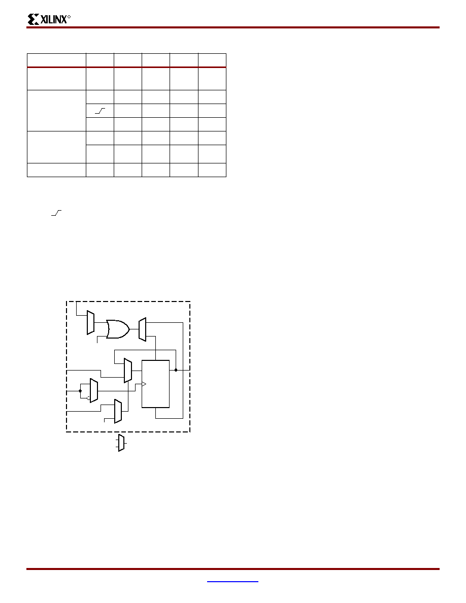
Configurable Logic Blocks (CLBs)
The CLBs are used to implement most of the logic in an
FPGA. The principal CLB elements are shown in the simpli-
fied block diagram in
Figure 2
. There are three look-up
tables (LUT) which are used as logic function generators,
two flip-flops and two groups of signal steering multiplexers.
There are also some more advanced features provided by
the CLB which will be covered in the
Advanced Features
Description, page 13
.
Function Generators
Two 16 x 1 memory look-up tables (F-LUT and G-LUT) are
used to implement 4-input function generators, each offer-
ing unrestricted logic implementation of any Boolean func-
tion of up to four independent input signals (F1 to F4 or G1
to G4). Using memory look-up tables the propagation delay
is independent of the function implemented.
A third 3-input function generator (H-LUT) can implement
any Boolean function of its three inputs. Two of these inputs
are controlled by programmable multiplexers (see box "A" of
Figure 2
). These inputs can come from the F-LUT or G-LUT
outputs or from CLB inputs. The third input always comes
from a CLB input. The CLB can, therefore, implement cer-
tain functions of up to nine inputs, like parity checking. The
three LUTs in the CLB can also be combined to do any arbi-
trarily defined Boolean function of five inputs.

Spartan and Spartan-XL Families Field Programmable Gate Arrays
4
www.xilinx.com
DS060 (v1.6) September 19, 2001
1-800-255-7778
Product Specification
R
A CLB can implement any of the following functions:
�
Any function of up to four variables, plus any second
function of up to four unrelated variables, plus any third
function of up to three unrelated variables
Note: When three separate functions are generated, one of
the function outputs must be captured in a flip-flop internal to
the CLB. Only two unregistered function generator outputs
are available from the CLB.
�
Any single function of five variables
�
Any function of four variables together with some
functions of six variables
�
Some functions of up to nine variables.
Implementing wide functions in a single block reduces both
the number of blocks required and the delay in the signal
path, achieving both increased capacity and speed.
The versatility of the CLB function generators significantly
improves system speed. In addition, the design-software
tools can deal with each function generator independently.
This flexibility improves cell usage.
Flip-Flops
Each CLB contains two flip-flops that can be used to regis-
ter (store) the function generator outputs. The flip-flops and
function generators can also be used independently (see
Figure 2
). The CLB input DIN can be used as a direct input
to either of the two flip-flops. H1 can also drive either
flip-flop via the H-LUT with a slight additional delay.
The two flip-flops have common clock (CK), clock enable
(EC) and set/reset (SR) inputs. Internally both flip-flops are
also controlled by a global initialization signal (GSR) which
is described in detail in
Global Signals: GSR and GTS,
page 20
.
Latches (Spartan-XL only)
The Spartan-XL CLB storage elements can also be config-
ured as latches. The two latches have common clock (K)
and clock enable (EC) inputs. Functionality of the storage
element is described in
Table 2
.
Figure 2: Spartan/XL Simplified CLB Logic Diagram (some features not shown)
G4
G
H1
F
G4
G3
G3
G2
G2
G1
D
YQ
Y
X
SR
CK
EC
Q
G1
SR
H1
DIN
G
H
Logic
Function
of
G1-G4
Logic
Function
of
F-G-H1
Multiplexer Controlled
by Configuration Program
G-LUT
F4
F4
F3
F3
F2
F2
F1
F1
K
EC
G
Logic
Function
of
F1-F4
F-LUT
H-LUT
A
B
D
XQ
SR
CK
EC
Q
DS060_02_0506 01
Spartan and Spartan-XL Families Field Programmable Gate Arrays
DS060 (v1.6) September 19, 2001
www.xilinx.com
5
Product Specification
1-800-255-7778
R
.
Clock Input
Each flip-flop can be triggered on either the rising or falling
clock edge. The CLB clock line is shared by both flip-flops.
However, the clock is individually invertible for each flip-flop
(see CK path in
Figure 3
). Any inverter placed on the clock
line in the design is automatically absorbed into the CLB.
Clock Enable
The clock enable line (EC) is active High. The EC line is
shared by both flip-flops in a CLB. If either one is left discon-
nected, the clock enable for that flip-flop defaults to the
active state. EC is not invertible within the CLB. The clock
enable is synchronous to the clock and must satisfy the
setup and hold timing specified for the device.
Set/Reset
The set/reset line (SR) is an asynchronous active High con-
trol of the flip-flop. SR can be configured as either set or
reset at each flip-flop. This configuration option determines
the state in which each flip-flop becomes operational after
configuration. It also determines the effect of a GSR pulse
during normal operation, and the effect of a pulse on the SR
line of the CLB. The SR line is shared by both flip-flops. If
SR is not specified for a flip-flop the set/reset for that flip-flop
defaults to the inactive state. SR is not invertible within the
CLB.
CLB Signal Flow Control
In addition to the H-LUT input control multiplexers (shown in
box "A" of
Figure 2, page 4
) there are signal flow control
multiplexers (shown in box "B" of
Figure 2
) which select the
signals which drive the flip-flop inputs and the combinatorial
CLB outputs (X and Y).
Each flip-flop input is driven from a 4:1 multiplexer which
selects among the three LUT outputs and DIN as the data
source.
Each combinatorial output is driven from a 2:1 multiplexer
which selects between two of the LUT outputs. The X output
can be driven from the F-LUT or H-LUT, the Y output from
G-LUT or H-LUT.
Control Signals
There are four signal control multiplexers on the input of the
CLB. These multiplexers allow the internal CLB control sig-
nals (H1, DIN, SR, and EC in
Figure 2
and
Figure 4
) to be
driven from any of the four general control inputs (C1-C4 in
Figure 4
) into the CLB. Any of these inputs can drive any of
the four internal control signals.
Table 2: CLB Storage Element Functionality
Mode
CK
EC
SR
D
Q
Power-Up or
GSR
X
X
X
X
SR
Flip-Flop
Operation
X
X
1
X
SR
1*
0*
D
D
0
X
0*
X
Q
Latch
Operation
(Spartan-XL)
1
1*
0*
X
Q
0
1*
0*
D
D
Both
X
0
0*
X
Q
Legend:
X
Don't care
Rising edge (clock not inverted).
SR
Set or Reset value. Reset is default.
0*
Input is Low or unconnected (default
value)
1*
Input is High or unconnected (default
value)
Figure 3: CLB Flip-Flop Functional Block Diagram
Multiplexer Controlled
by Configuration Program
D
Q
Q
D
GND
GSR
Vcc
CK
EC
SR
SD
RD
DS060_03_041901