
2-71
XC4000A
Logic Cell Array Family
Æ
Product Specifications
Description
The XC4000A family of FPGAs offers four devices at the low
end of the XC4000 family complexity range. XC4000A
differs from XC4000 in four areas: fewer routing resources,
fewer wide-edge decoders, higher output sink current, and
improved output slew-rate control.
∑
The XC4000 routing structure is optimized for smaller
designs, naturally requiring fewer routing resources. The
XC4000A devices have four Longlines and four single-
length lines per row and column, while the XC4000
devices have six Longlines and eight single-length lines
per row and column. This results in a smaller chip area
and lower cost per device.
∑
XC4000A has two wide-edge decoders on every device
edge, while the XC4000 has four. All other wide-decoder
features are identical in XC4000 and XC4000A.
∑
XC4000A outputs are specified at 24 mA, sink current,
while XC4000 outputs are specified at 12 mA. The source
current is the same 4 mA for both families.
∑
The XC4000A family offers a more sophisticated output
slew-rate control structure with four configurable options
for each individual output driver: fast, medium fast, me-
dium slow, and slow. Slew-rate control can alleviate
ground-bounce problems when multiple outputs switch
simultaneously, and it can reduce or eliminate crosstalk
and transmission-line effects on printed circuit boards.
Note that the XC4003 and XC4005 devices are available in
both flavors, the lower-priced XC4003A/XC4005A with re-
duced routing, and the higher-priced XC4003/XC4005 with
more abundant routing resources. The XC4000A devices
are intended for less demanding and more structured
designs, and the XC4000 devices for more random designs
requiring additional routing resources.
The equivalent devices are pin-compatible and are avail-
able in identical packages, but they are not bitstream
compatible. In order to move from a XC4000A to a XC4000,
or vice versa, the design must be recompiled.
Features
∑
Third Generation Field-Programmable Gate Arrays
≠ Abundant flip-flops
≠ Flexible function generators
≠ On-chip ultra-fast RAM
≠ Dedicated high-speed carry-propagation circuit
≠ Wide edge decoders (two per edge)
≠ Hierarchy of interconnect lines
≠ Internal 3-state bus capability
≠ Eight global low-skew clock or signal distribution
network
∑
Flexible Array Architecture
≠ Programmable logic blocks and I/O blocks
≠ Programmable interconnects and wide decoders
∑
Sub-micron CMOS Process
≠ High-speed logic and Interconnect
≠ Low power consumption
∑
Systems-Oriented Features
≠ IEEE 1149.1-compatible boundary-scan logic support
≠ Programmable output slew rate (4 modes)
≠ Programmable input pull-up or pull-down resistors
≠ 24-mA sink current per output (48 per pair)
∑
Configured by Loading Binary File
≠ Unlimited reprogrammability
≠ Six programming modes
∑
XACT Development System runs on '386/'486-type PC,
NEC PC, Apollo, Sun-4, and Hewlett-Packard 700 Series
≠ Interfaces to popular design environments like
Viewlogic, Mentor Graphics and OrCAD
≠ Fully automatic partitioning, placement and routing
≠ Interactive design editor for design optimization
≠ 288 macros, 34 hard macros, RAM/ROM compiler
Device
XC4002A
XC4003A
XC4004A
XC4005A
Appr. Gate Count
2,000
3,000
4,000
5,000
CLB Matrix
8 x 8
10 x 10
12 x 12
14 x 14
Number of CLBs
64
100
144
196
Number of Flip-Flops
256
360
480
616
Max Decode Inputs (per side)
24
30
36
42
Max RAM Bits
2,048
3,200
4,608
6,272
Number of IOBs
64
80
96
112
Table 1. The XC4000A Family of Field-Programmable Gate Arrays

XC4000A Logic Cell Array Family
2-72
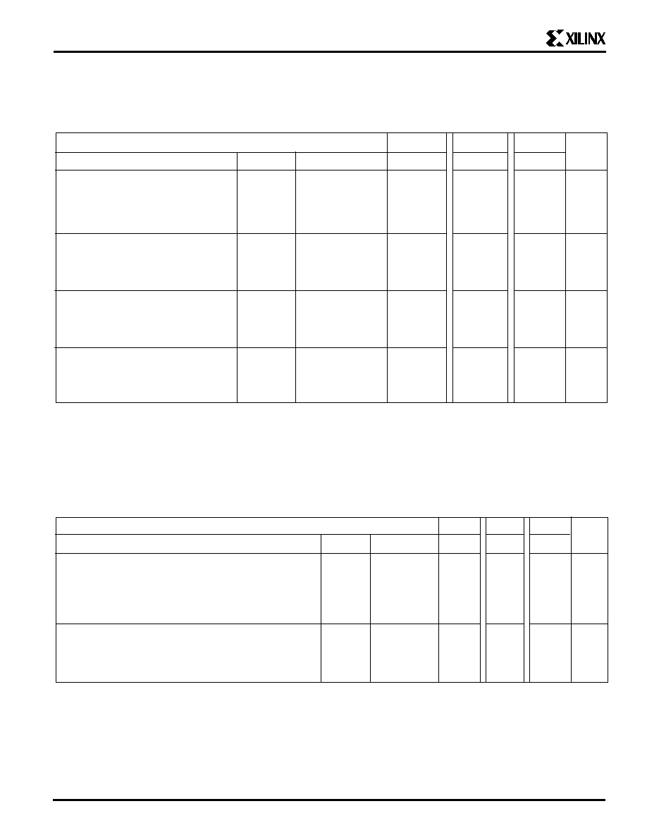
Absolute Maximum Ratings
Symbol Description
Units
V
CC
Supply voltage relative to GND
≠0.5 to +7.0
V
V
IN
Input voltage with respect to GND
≠0.5 to V
CC
+0.5
V
V
TS
Voltage applied to 3-state output
≠0.5 to V
CC
+0.5
V
T
STG
Storage temperature (ambient)
≠65 to + 150
∞
C
T
SOL
Maximum soldering temperature (10 s @ 1/16 in. = 1.5 mm)
+ 260
∞
C
T
J
Junction temperature
+ 150
∞
C
Note:
Stresses beyond those listed under Absolute Maximum Ratings may cause permanent damage to the device.
These are stress ratings only, and functional operation of the device at these or any other conditions beyond those
listed under Recommended Operating Conditions is not implied. Exposure to Absolute Maximum Ratings conditions
for extended periods of time may affect device reliability.
Operating Conditions
Symbol
Description
Min
Max
Units
V
CC
Supply voltage relative to GND Commercial 0
∞
C to 85
∞
C junction
4.75
5.25
V
Supply voltage relative to GND Industrial -40
∞
C to 100
∞
C junction
4.5
5.5
V
Supply voltage relative to GND
Military ≠55
∞
C to 125
∞
C case
4.5
5.5
V
V
IH
High-level input voltage (XC4000 has TTL-like input thresholds)
2.0
V
CC
V
V
IL
Low-level input voltage (XC4000 has TTL-like input thresholds)
0
0.8
V
T
IN
Input signal transition time
250
ns
DC Characteristics Over Operating Conditions
Symbol
Description
Min
Max
Units
V
OH
High-level output voltage @ I
OH
= ≠4.0 mA, V
CC
min
2.4
V
V
OL
Low-level output voltage @ I
OL
= 24 mA, V
CC
min (Note 1)
0.4
V
I
CCO
Quiescent LCA supply current (Note 2)
10
mA
I
IL
Leakage current
≠10
+10
µ
A
C
IN
Input capacitance (sample tested)
15
pF
I
RIN
Pad pull-up (when selected) @ V
IN
= 0V (sample tested)
0.02
0.25
mA
I
RLL
Horizontal Long Line pull-up (when selected) @ logic Low
0.2
2.5
mA
Note: 1. With 50% of the outputs simultaneously sinking 24 mA.
2. With no output current loads, no active input or longline pull-up resistors, all package pins at V
CC
or GND, and
the LCA configured with a MakeBits tie option.
At junction temperatures above those listed as Operating conditions, all delay parameters increase by 0.35% per
∞
C.
2-73
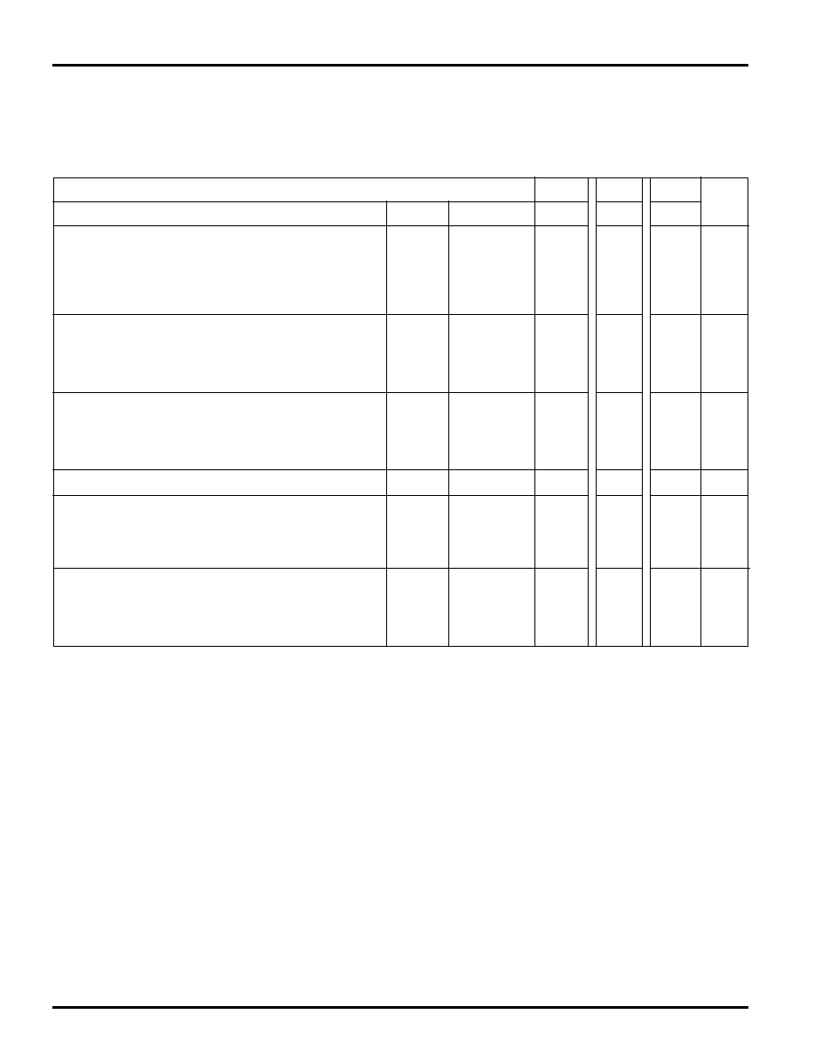
PRELIMINARY
Speed Grade
-6
-5
-4
Description
Symbol
Device
Max
Max
Max
Units
Global Signal Distribution
From pad through primary buffer, to any clock k
T
PG
XC4002A
7.7
5.7
ns
XC4003A
7.8
5.8
5.1
ns
XC4004A
7.9
5.9
ns
XC4005A
8.0
6.0
5.5
ns
From pad through secondary buffer, to any clock k
T
SG
XC4002A
8.7
6.7
ns
XC4003A
8.8
6.8
6.3
ns
XC4004A
8.9
6.9
ns
XC4005A
9.0
7.0
6.7
ns
PRELIMINARY
Wide Decoder Switching Characteristic Guidelines
Testing of the switching parameters is modeled after testing methods specified by MIL-M-38510/605. All devices are 100% functionally
tested. Since many internal timing parameters cannot be measured directly, there derived from benchmark timing patterns. The following
guidelines relflect worst-case values over the recommended operating conditions. For more detailed, more precise, and more up-to-date
timing information, use the values provided by the XACT timing calculator and used in the simulator.
Speed Grade
-6
-5
-4
Description
Symbol
Device
Max
Max
Max
Units
Full length, both pull-ups,
T
WAF
XC4002A
8.5
7.5
ns
inputs from IOB I-pins
XC4003A
9.0
8.0
5.0
ns
XC4004A
9.5
8.5
ns
XC4005A
10.0
9.0
6.0
ns
Full length, both pull-ups
T
WAFL
XC4002A
11.5
10.5
ns
inputs from internal logic
XC4003A
12.0
11.0
7.0
ns
XC4004A
12.5
11.5
ns
XC4005A
13.0
12.0
8.0
ns
Half length, one pull-up
T
WAO
XC4002A
8.5
7.5
ns
inputs from IOB I-pins
XC4003A
9.0
8.0
6.0
ns
XC4004A
9.5
8.5
ns
XC4005A
10.0
9.0
7.0
ns
Half length, one pull-up
T
WAOL
XC4002A
11.5
10.5
ns
inputs from internal logic
XC4003A
12.0
11.0
8.0
ns
XC4004A
12.5
11.5
ns
XC4005A
13.0
12.0
9.0
ns
Note: These delays are specified from the decoder input to the decoder output. For pin-to-pin delays, add the input delay (T
PID
)
and output delay (one of 4 modes), as listed on page 2-70.
Global Buffer Switching Characteristic Guidelines
Testing of the switching parameters is modeled after testing methods specified by MIL-M-38510/605. All devices are 100% functionally
tested. Since many internal timing parameters cannot be measured directly, they are derived from benchmark timing patterns. The
following guidelines reflect worst-case values over the recommended operating conditions. For more detailed, more precise, and more
up-to-date timing information, use the values provided by the XACT timing calculator and used in the simulator.
XC4000A Logic Cell Array Family
2-74
PRELIMINARY
Speed Grade
-6
-5
-4
Description
Symbol
Device
Max
Max
Max
Units
TBUF driving a Horizontal Longline (L.L.)
I going High or Low to L.L. going High or Low,
T
IO1
XC4002A
8.2
6.0
ns
while T is Low, i.e. buffer is constantly active
XC4003A
8.8
6.2
4.4
ns
XC4004A
9.4
6.6
ns
XC4005A
10.0
7.0
5.5
ns
I
going Low to L.L. going from resistive pull-up
T
IO2
XC4002A
8.7
6.5
ns
High to active Low, (TBUF configured as open drain)
XC4003A
9.3
6.7
5.0
ns
XC4004A
9.9
7.1
ns
XC4005A
10.5
7.5
6.0
ns
T
going Low to L.L. going from resistive pull-up
T
ON
XC4002A
10.1
8.4
ns
or floating High to active Low, (TUBF configured
XC4003A
10.7
9.0
7.2
ns
as open drain)
XC4004A
11.4
9.5
ns
XC4005A
12.0
10.0
8.0
ns
T
going High to TBUF going inactive, not driving L.L.
T
OFF
All devices
3.0
2.0
1.8
ns
T
going High to L.L. going from Low to High,
T
PUS
XC4002A
23.0
19.0
ns
pulled up by a single resistor
XC4003A
24.0
20.0
14.0
ns
XC4004A
25.0
21.0
ns
XC4005A
26.0
22.0
16.0
ns
T
going High to L.L. going from Low to High,
T
PUF
XC4002A
10.5
8.5
ns
pulled up by two resistors
XC4003A
11.0
9.0
7.0
ns
XC4004A
11.5
9.5
ns
XC4005A
12.0
10.0
8.0
ns
Horizontal Longline Switching Characteristic Guidelines
Testing of the switching parameters is modeled after testing methods specified by MIL-M-38510/605. All devices are 100% functionally
tested. Since many internal timing parameters cannot be measured directly, they are derived from benchmark timing patterns. The
following guidelines reflect worst-case values over the recommended operating conditions. For more detailed, more precise, and more
up-to-date timing information, use the values provided by the XACT timing calculator and used in the simulator.

2-75
PRELIMINARY
Speed Grade
-6
-5
-4
Description
Symbol
Device
Units
Global Clock to Output (fast)
T
ICKOF
XC4002A
14.9
12.2
ns
XC4003A
15.1
12.5
11.6
ns
(Max)
XC4004A
15.3
12.8
ns
XC4005A
15.5
13.0
12.0
ns
Global Clock to Output (slew limited)
T
ICKO
XC4002A
19.9
15.2
ns
XC4003A
20.1
15.5
14.6
ns
(Max)
XC4004A
20.3
15.8
ns
XC4005A
20.5
16.0
15.0
ns
Input Set-up Time, using IFF (no delay)
T
PSUF
XC4002A
2.6
2.3
ns
XC4003A
2.4
2.0
1.6
ns
(Min)
XC4004A
2.2
1.7
ns
XC4005A
2.0
1.5
1.2
ns
Input Hold time, using IFF (no delay)
T
PHF
XC4002A
4.9
3.7
ns
XC4003A
5.1
4.0
4.0
ns
(Min)
XC4004A
5.3
4.3
ns
XC4005A
5.5
4.5
4.5
ns
Input Set-up Time, using IFF (with delay)
T
PSU
XC4002A
21.8
18.8
ns
XC4003A
21.5
18.5
12.0
ns
(Min)
XC4004A
21.2
18.2
ns
XC4005A
21.0
18.0
12.0
ns
Input Hold Time, using IFF (with delay)
T
PH
XC4002A
0
0
ns
XC4003A
0
0
0
ns
(Min)
XC4004A
0
0
ns
XC4005A
0
0
0
ns
Guaranteed Input and Output Parameters (Pin-to-Pin)
All values listed below are tested directly. and guaranteed over the operating conditions. The same parameters can also be derived
indirectly from the IOB and Global Buffer specifications. The XACT delay calculator uses this indirect method. When there is a discrepancy
between these two methods, the directly tested values listed below should be used, and the derived values should be ignored.
IFF
Input
Set-Up
&
Hold
Time
OFF
∑
∑
∑
∑
∑
Global Clock-to-Output Delay
X3192
T
PG
Timing is measured at pin threshold, with 50 pF external
capacitive loads (incl. test fixture). When testing fast out-
puts, only one output switches. When testing slew-rate
limited outputs, half the number of outputs on one side of the
device are switching. These parameter values are tested
and guaranteed for worst-case conditions of supply voltage
and temperature, and also with the most unfavorable clock
polarity choice.
PRELIMINARY
PRELIMINARY
Pad to I1, I2
via transparent
latch, with delay
XC4003A 17.6 ns
XC4005A 17.9 ns
T
PDLI
for -4 Speed Grade
Input set-up time
pad to clock (IK)
with delay
XC4003A 15.6 ns
XC4005A 15.9 ns
T
PICKD
for -4 Speed Grade
X6091
See page 2-76

XC4000A Logic Cell Array Family
2-76
PRELIMINARY
-6
-5
Description
Symbol
Min Max
Min Max
Min Max Units
INPUT
Propagation Delays
Pad to I1, I2
T
PID
4.0
3.0
2.8
ns
Pad to I1, I2, via transparent latch (no delay)
T
PLI
8.0
7.0
6.0
ns
Pad to I1, I2, via transparent latch (with delay)
T
PDLI
26.0
24.0
**
ns
Clock (IK) toI1, I2, (flip-flop)
T
IKRI
8.0
7.0
6.0
ns
Clock (IK) to I1, I2 (latch enable, active Low)
T
IKLI
8.0
7.0
6.0
ns
Set-up Time (Note 3)
Pad to Clock (IK), no delay
T
PICK
7.0
6.0
4.0
ns
Pad to Clock (IK) with delay
T
PICKD
25.0
24 .0
**
ns
Hold Time (Note 3)
Pad to Clock (IK), no delay
T
IKPI
1.0
1.0
1.0
ns
Pad to Clock (IK) with delay
T
IKPID
neg
neg
neg
ns
OUTPUT
Propagation Delays
Clock (OK) to Pad (fast)
T
OKPOF
7.5
7.0
6.5
ns
Output (O) to Pad (fast)
T
OPF
9.0
7.0
5.5
ns
3-state to Pad begin hi-Z (slew-rate independent)
T
TSHZ
9.0
7.0
6.5
ns
3-state to Pad active and valid (fast)
T
TSONF
13.0
10.0
9.5
ns
Additional Delay
For medium fast outputs
2.0
1.5
1.0
ns
For medium slow outputs
4.0
3.0
2.0
ns
For slow outputs
6.0
4.5
3.0
ns
Set-up and Hold Times
Output (O) to clock (OK) set-up time
T
OOK
8.0
6.0
5.5
ns
Output (O) to clock (OK) hold time
T
OKO
0.0
0.0
0
ns
Clock
Clock High or Low time
T
CH/
T
CL
5.0
4.0
4.0
ns
Global Set/Reset
Delay from GSR net through Q to I1, I2
T
RRI
14.5
13.5
13.5
ns
Delay from GSR net to Pad
T
RPO
18.0
17.0
14.6
ns
GSR width*
T
MRW
21.0
18.0
18.0
ns
IOB Switching Characteristic Guidelines
Testing of the switching parameters is modeled after testing methods specified by MIL-M-38510/605. All devices are 100% functionally
tested. Since many internal timing parameters cannot be measured directly, they are derived from benchmark timing patterns. The following
guidelines reflect worst-case values over the recommended operating conditions. For more detailed, more precise, and more up-to-date
timing information, use the values provided by the XACT timing calculator and used in the simulator.
* Timing is based on the XC4005. For other devices see XACT timing calculator.
** See preceding page.
Notes: 1. Timing is measured at pin threshold, with 50 pF external capacitive loads (incl. test fixture).
2. Voltage levels of unused (bonded and unbonded) pads must be valid logic levels. Each can be configured with the
internal pull-up or pull-down resistor or alternatively configured as a driven output or be driven from an external source.
3. Input pad setup times and hold times are specified with respect to the internal clock (IK). To calculate system setup time,
subtract clock delay (clock pad to IK) from the specified input pad setup time value, but do not subtract below zero.
Negative hold time means that the delay in the input data is adequate for the external system hold time to be zero,
provided the input clock uses the Global signal distribution from pad to IK.
-4
XC4003A
XC4005A

2-77
PRELIMINARY
Speed Grade
-6
-5
-4
Description
Symbol
Min Max
Min
Max
Min Max Units
Combinatorial Delays
F/G inputs to X/Y outputs
T
ILO
6.0
4.5
4.0
ns
F/G inputs via H' to X/Y outputs
T
IHO
8.0
7.0
6.0
ns
C inputs via H' to X/Y outputs
T
HHO
7.0
5.0
4.5
ns
CLB Fast Carry Logic
Operand inputs (F1,F2,G1,G4) to C
OUT
T
OPCY
7.0
5.5
5.0
ns
Add/Subtract input (F3) to C
OUT
T
ASCY
8.0
6.0
5.5
ns
Initialization inputs (F1,F3) to C
OUT
T
INCY
6.0
4.0
3.5
ns
C
IN
through function generators to X/Y outputs
T
SUM
8.0
6.0
5.5
ns
C
IN
to C
OUT
, bypass function generators.
T
BYP
2.0
1.5
1.5
ns
Sequential Delays
Clock K to outputs Q
T
CKO
5.0
3.0
3.0
ns
Set-up Time before Clock K
F/G inputs
T
ICK
6.0
4.5
4.5
ns
F/G inputs via H'
T
IHCK
8.0
6.0
6.0
ns
C inputs via H1
T
HHCK
7.0
5.0
5.0
ns
C inputs via DIN
T
DICK
4.0
3.0
3.0
ns
C inputs via EC
T
ECCK
7.0
4.0
3.0
ns
C inputs via S/R, going Low (inactive)
T
RCK
6.0
4.5
4.0
ns
C
IN
input via F'/G'
8.0
6.0
5.5
ns
C
IN
input via F'/G' and H'
10.0
7.5
7.3
ns
Hold Time after Clock K
F/G inputs
T
CKI
0
0
0
ns
F/G inputs via H'
T
CKIH
0
0
0
ns
C inputs via H1
T
CKHH
0
0
0
ns
C inputs via DIN
T
CKDI
0
0
0
ns
C inputs via EC
T
CKEC
0
0
0
ns
C inputs via S/R, going Low (inactive)
T
CKR
0
0
0
ns
Clock
Clock High time
T
CH
5.0
4.0
4.0
ns
Clock Low time
T
CL
5.0
4.0
4.0
ns
Set/Reset Direct
Width (High)
T
RPW
5.0
4.0
4.0
ns
Delay from C inputs via S/R, going High to Q
T
RIO
9.0
8.0
7.0
ns
Master Set/Reset*
Width (High or Low)
T
MRW
21.0
18.0
18.0
ns
Delay from Global Set/Reset net to Q
T
MRQ
33.0
31.0
28.0
ns
CLB Switching Characteristic Guidelines
Testing of the switching parameters is modeled after testing methods specified by MIL-M-38510/605. All devices are 100% functionally
tested. Since many internal timing parameters cannot be measured directly, they are derived from benchmark timing patterns. The following
guidelines reflect worst-case values over the recommended operating conditions. For more detailed, more precise, and more up-to-date
timing information, use the values provided by the XACT timing calculator and used in the simulator.
* Timing is based on the XC4005. For other devices see XACT timing calculator.
XC4003A
XC4005A

XC4000A Logic Cell Array Family
2-78
PRELIMINARY
Write Operation
Address write cycle time
16 x 2
T
WC
9.0
8.0
8.0
ns
32 x 1
T
WCT
9.0
8.0
8.0
ns
Write Enable pulse width (High)
16 x 2
T
WP
5.0
4.0
4.0
ns
32 x 1
T
WPT
5.0
4.0
4.0
ns
Address set-up time before beginning of WE
16 x 2
T
AS
2.0
2.0
2.0
ns
32 x 1
T
AST
2.0
2.0
2.0
ns
Address hold time after end of WE
16 x 2
T
AH
2.0
2.0
2.0
ns
32 x 1
T
AHT
2.0
2.0
2.0
ns
DIN set-up time before end of WE
16 x 2
T
DS
4.0
4.0
4.0
ns
32 x 1
T
DST
5.0
5.0
5.0
ns
DIN hold time after end of WE
both
T
DHT
2.0
2.0
2.0
ns
Read Operation
Address read cycle time
16 x 2
T
RC
7.0
5.5
5.0
ns
32 x 1
T
RCT
10.0
7.5
7.0
ns
Data valid after address change
16 x 2
T
ILO
6.0
4.5
4.0
ns
(no Write Enable)
32 x 1
T
IHO
8.0
7.0
6.0
ns
Read Operation, Clocking Data into Flip-Flop
Address setup time before clock K
16 x 2
T
ICK
6.0
4.5
4.5
ns
32 x 1
T
IHCK
8.0
6.0
6.0
ns
Read During Write
Data valid after WE going active
16 x 2
T
WO
12.0
10.0
9.0
ns
(DIN stable before WE)
32 x 1
T
WOT
15.0
12.0
11.0
ns
Data valid after DIN
16 x 2
T
DO
11.0
9.0
8.5
ns
(DIN change during WE)
32 x 1
T
DOT
14.0
11.0
11.0
ns
Read During Write, Clocking Data into Flip-Flop
WE setup time before clock K
16 x 2
T
WCK
12.0
10.0
9.5
ns
32 x 1
T
WCKT
15.0
12.0
11.5
ns
Data setup time before clock K
16 x 2
T
DCK
11.0
9.0
9.0
ns
32 x 1
T
DCKT
14.0
11.0
11.0
ns
CLB Switching Characteristic Guidelines (continued)
Testing of the switching parameters is modeled after testing methods specified by MIL-M-38510/605. All devices are 100% functionally
tested. Since many internal timing parameters cannot be measured directly, they are derived from benchmark timing patterns. The following
guidelines reflect worst-case values over the recommended operating conditions. For more detailed, more precise, and more up-to-date
timing information, use the values provided by the XACT timing calculator and used in the simulator.
CLB RAM OPTION
Speed Grade
-6
-5
-4
Description
Symbol
Min
Max
Min Max
Min Max Units
Note: Timing for the 16 x 1 RAM option is identical to 16 x 2 RAM timing
XC4003A
XC4005A

2-79
CLB RAM Timing Characteristics
RC
T
ILO
T
VALID
VALID
ADDRESS
X,Y OUTPUTS
READ
CLOCK
XQ,YQ OUTPUTS
READ DURING WRITE
ICK
T
CKO
T
WP
T
VALID
VALID
WO
T
WRITE ENABLE
DATA IN
(stable during WE)
X,Y OUTPUTS
DATA IN
(changing during WE)
X,Y OUTPUTS
OLD
NEW
WO
T
VALID
(OLD)
DO
T
VALID
(NEW)
WRITE ENABLE
DATA IN
CLOCK
XQ,YQ OUTPUTS
WRITE ENABLE
DATA IN
READ DURING WRITE, CLOCKING DATA INTO FLIP-FLOP
WRITE
WP
T
WCK
T
DCK
T
CKO
T
AS
T
WP
T
DS
T
DH
T
X2640
REQUIRED
DH
T
VALID
(PREVIOUS)
CH
T
VALID
(NEW)
VALID
(OLD)
AH
T
READ, CLOCKING DATA INTO FLIP-FLOP

XC4000A Logic Cell Array Family
2-80

2-81
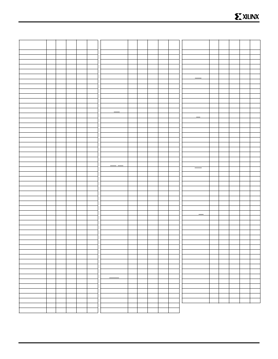
XC4002A Pinouts
*
Indicates unconnected package pins.
Contributes only one bit (.i) to the boundary scan register.
Boundary Scan Bit 0 = TDO.T
Boundary Scan Bit 1 = TDO.O
Boundary Scan Bit 199 = BSCANT.UPD
Pin
Description
Bound
Scan
Pin
Description
Bound
Scan
Pin
Description
Bound
Scan
PC 84 PQ100 VQ100 PG120
PC 84 PQ100 VQ100 PG120
PC 84 PQ100 VQ100 PG120
VCC
2
92
89
G3
≠
I/O
28
23
20
C9
92
≠
≠
≠
≠
L9
≠
I/O (A8)
3
93
90
G1
26
SGCK2 (I/O)
29
24
21
A12
95
I/O (D6)
58
58
55
M10
157
I/O (A9)
4
94
91
F1
29
O (M1)
30
25
22
B11
98
I/O
≠
59
56
N11
160
≠
≠
95
*
92
*
E1
*
≠
GND
31
26
23
C10
≠
I/O (D5)
59
60
57
M9
163
≠
≠
96
*
93
*
F2
*
≠
I (M0)
32
27
24
C11
101
I/O (
CSO
)
60
61
58
N10
166
I/O (A10)
5
97
94
F3
32
VCC
33
28
25
D11
≠
≠
≠
62
*
59
*
L8
*
≠
I/O (A11)
6
98
95
D1
35
I (M2)
34
29
26
B12
102
≠
≠
63
*
60
*
N9
*
≠
≠
≠
≠
≠
E2
*
≠
PGCK2 (I/O)
35
30
27
C12
103
I/O (D4)
61
64
61
M8
169
I/O (A12)
7
99
96
C1
38
I/O (HDC)
36
31
28
A13
106
I/O
62
65
62
N8
172
I/O (A13)
8
100
97
D2
41
≠
≠
≠
≠
B13
*
≠
VCC
63
66
63
M7
≠
≠
≠
≠
≠
E3
*
≠
≠
≠
≠
≠
E11
*
≠
GND
64
67
64
L7
≠
≠
≠
≠
≠
B1
*
≠
I/O
≠
32
29
D12
109
I/O (D3)
65
68
65
N7
175
I/O (A14)
9
1
98
C2
44
I/O (
LDC
)
37
33
30
C13
112
I/O (
RS
)
66
69
66
N6
178
SGCK1 (A15, I/O)
10
2
99
D3
47
I/O
38
34
31
E12
115
≠
≠
70
*
67
*
N5
*
≠
VCC
11
3
100
C3
≠
I/O
39
35
32
D13
118
≠
≠
≠
≠
M6
*
≠
GND
12
4
1
C4
≠
≠
≠
36
*
33
*
F11
*
≠
I/O (D2)
67
71
68
L6
181
PGCK1 (A16, I/O)
13
5
2
B2
50
≠
≠
37
*
34
*
E13
*
≠
I/O
68
72
69
N4
184
I/O (A17)
14
6
3
B3
53
I/O
40
38
35
F12
121
I/O (D1)
69
73
70
M5
187
≠
≠
≠
≠
A1
*
≠
I/O (
ERR
,
INIT
)
41
39
36
F13
124
I/O (RCLK-BUSY/RDY)
70
74
71
N3
190
≠
≠
≠
≠
A2
*
≠
VCC
42
40
37
G12
≠
≠
≠
≠
≠
M4
*
≠
I/O (TDI)
15
7
4
C5
56
GND
43
41
38
G11
≠
≠
≠
≠
≠
L5
*
≠
I/O (TCK)
16
8
5
B4
59
I/O
44
42
39
G13
127
I/O (D0, DIN)
71
75
72
N2
193
≠
≠
≠
≠
A3
*
≠
I/O
45
43
40
H13
130
SGCK4 (DOUT, I/O)
72
76
73
M3
196
I/O (TMS)
17
9
6
B5
62
≠
≠
44
*
41
*
J13
*
≠
CCLK
73
77
74
L4
≠
I/O
18
10
7
A4
65
≠
≠
45
*
42
*
H12
*
≠
VCC
74
78
75
L3
≠
≠
≠
≠
≠
C6
*
≠
I/O
46
46
43
H11
133
O (TDO)
75
79
76
M2
≠
≠
≠
11
*
8
*
A5
*
≠
I/O
47
47
44
K13
136
GND
76
80
77
K3
≠
I/O
19
12
9
B6
68
I/O
48
48
45
J12
139
I/O (A0,
WS
)
77
81
78
L2
2
I/O
20
13
10
A6
71
I/O
49
49
46
L13
142
PGCK4 (I/O,A1)
78
82
79
N1
5
GND
21
14
11
B7
≠
≠
≠
≠
≠
K12
*
≠
≠
≠
≠
≠
M1
*
≠
VCC
22
15
12
C7
≠
≠
≠
≠
≠
J11
*
≠
≠
≠
≠
≠
J3
*
≠
I/O
23
16
13
A7
74
I/O
50
50
47
M13
145
I/O (CS1, A2)
79
83
80
K2
8
I/O
24
17
14
A8
77
SGCK3 (I/O)
51
51
48
L12
148
I/O (A3)
80
84
81
L1
11
≠
≠
18
*
15
*
A9
*
≠
GND
52
52
49
K11
≠
I/O (A4)
81
85
82
J2
14
≠
≠
≠
≠
B8
*
≠
DONE
53
53
50
L11
≠
I/O (A5)
82
86
83
K1
17
I/O
25
19
16
C8
80
VCC
54
54
51
L10
≠
≠
≠
87
*
84
*
H3
*
≠
I/O
26
20
17
A10
83
PROG
55
55
52
M12
≠
≠
≠
88
*
85
*
J1
*
≠
I/O
27
21
18
B9
86
I/O (D7)
56
56
53
M11
151
I/O (A6)
83
89
86
H2
20
I/O
≠
22
19
A11
89
PGCK3 (I/O)
57
57
54
N13
154
I/O (A7)
84
90
87
H1
23
≠
≠
≠
≠
B10
*
≠
≠
≠
≠
≠
N12
*
≠
GND
1
91
88
G2
≠
This document was created with FrameMaker 4 0 2

XC4000A Logic Cell Array Family
2-82
XC4003A Pinouts
*
Indicates unconnected package pins.
Contributes only one bit (.i) to the boundary scan register.
Boundary Scan Bit 0 = TDO.T
Boundary Scan Bit 1 = TDO.O
Boundary Scan Bit 247 = BSCANT.UPD
Pin
Description
Bound
Scan
Pin
Description
Bound
Scan
PC84
VQ100 PQ100 PG120
PC84
VQ100 PQ100 PG120
VCC
2
89
92
G3
≠
GND
43
38
41
G11
≠
I/O (A8)
3
90
93
G1
32
I/O
44
39
42
G13
157
I/O (A9)
4
91
94
F1
35
I/O
45
40
43
H13
160
I/O
≠
92
95
E1
38
I/O
≠
41
44
J13
163
I/O
≠
93
96
F2
41
I/O
≠
42
45
H12
166
I/O (A10)
5
94
97
F3
44
I/O
46
43
46
H11
169
I/O (A11)
6
95
98
D1
47
I/O
47
44
47
K13
172
≠
≠
≠
≠
E2
*
≠
I/O
48
45
48
J12
175
I/O (A12)
7
96
99
C1
50
I/O
49
46
49
L13
178
I/O (A13)
8
97
100
D2
53
≠
≠
≠
≠
K12
*
≠
≠
≠
≠
≠
E3
*
≠
≠
≠
≠
≠
J11
*
≠
≠
≠
≠
≠
B1
*
≠
I/O
50
47
50
M13
181
I/O (A14)
9
98
1
C2
56
SGCK3 (I/O)
51
48
51
L12
184
SGCK1 (A15,I/O)
10
99
2
D3
59
GND
52
49
52
K11
≠
VCC
11
100
3
C3
≠
DONE
53
50
53
L11
≠
GND
12
1
4
C4
≠
VCC
54
51
54
L10
≠
PGCK1 (A16, I/O)
13
2
5
B2
62
PROG
55
52
55
M12
≠
I/O (A17)
14
3
6
B3
65
I/O (D7)
56
53
56
M11
187
≠
≠
≠
≠
A1
*
≠
PGCK3 (I/O)
57
54
57
N13
190
≠
≠
≠
≠
A2
*
≠
≠
≠
≠
≠
N12
*
≠
I/O (TDI)
15
4
7
C5
68
≠
≠
≠
≠
L9
*
≠
I/O (TCK)
16
5
8
B4
71
I/O (D6)
58
55
58
M10
193
≠
≠
≠
≠
A3
*
≠
I/O
≠
56
59
N11
196
I/O (TMS)
17
6
9
B5
74
I/O (D5)
59
57
60
M9
199
I/O
18
7
10
A4
77
I/O (CS0)
60
58
61
N10
202
I/O
≠
≠
≠
C6
80
I/O
≠
59
62
L8
205
I/O
≠
8
11
A5
83
I/O
≠
60
63
N9
208
I/O
19
9
12
B6
86
I/O (D4)
61
61
64
M8
211
I/O
20
10
13
A6
89
I/O
62
62
65
N8
214
GND
21
11
14
B7
≠
VCC
63
63
66
M7
≠
VCC
22
12
15
C7
≠
GND
64
64
67
L7
≠
I/O
23
13
16
A7
92
I/O (D3)
65
65
68
N7
217
I/O
24
14
17
A8
95
I/O (
RS
)
66
66
69
N6
220
I/O
≠
15
18
A9
98
I/O
≠
67
70
N5
223
I/O
≠
≠
≠
B8
101
I/O
≠
≠
≠
M6
226
I/O
25
16
19
C8
104
I/O (D2)
67
68
71
L6
229
I/O
26
17
20
A10
107
I/O
68
69
72
N4
232
I/O
27
18
21
B9
110
I/O (D1)
69
70
73
M5
235
I/O
≠
19
22
A11
113
I/O (RCLK-BUSY/RDY)
70
71
74
N3
238
≠
≠
≠
≠
B10
*
≠
≠
≠
≠
≠
M4
*
≠
I/O
28
20
23
C9
116
≠
≠
≠
≠
L5
*
≠
SGCK2 (I/O)
29
21
24
A12
119
I/O (D0, DIN)
71
72
75
N2
241
O (M1)
30
22
25
B11
122
SGCK4 (DOUT, I/O)
72
73
76
M3
244
GND
31
23
26
C10
≠
CCLK
73
74
77
L4
≠
I (M0)
32
24
27
C11
125
VCC
74
75
78
L3
≠
VCC
33
25
28
D11
≠
O (TDO)
75
76
79
M2
≠
I (M2)
34
26
29
B12
126
GND
76
77
80
K3
≠
PGCK2 (I/O)
35
27
30
C12
127
I/O (A0,
WS
)
77
78
81
L2
2
I/O (HDC)
36
28
31
A13
130
PGCK4 (A1, I/O)
78
79
82
N1
5
≠
≠
≠
≠
B13
*
≠
≠
≠
≠
≠
M1
*
≠
≠
≠
≠
≠
E11
*
≠
≠
≠
≠
≠
J3
*
≠
I/O
≠
29
32
D12
133
I/O (CS1, A2)
79
80
83
K2
8
I/O (
LDC
)
37
30
33
C13
136
I/O (A3)
80
81
84
L1
11
I/O
38
31
34
E12
139
I/O (A4)
81
82
85
J2
14
I/O
39
32
35
D13
142
I/O (A5)
82
83
86
K1
17
I/O
≠
33
36
F11
145
I/O
≠
84
87
H3
20
I/O
≠
34
37
E13
148
I/O
≠
85
88
J1
23
I/O
40
35
38
F12
151
I/O (A6)
83
86
89
H2
26
I/O (
ERR
,
INIT
)
41
36
39
F13
154
I/O (A7)
84
87
90
H1
29
VCC
42
37
40
G12
≠
GND
1
88
91
G2
≠
2-83
XC4004A Pinouts
*
Indicates unconnected package pins.
Contributes only one bit (.i) to the boundary scan register.
Boundary Scan Bit 0 = TDO.T
Boundary Scan Bit 1 = TDO.O
Boundary Scan Bit 295 = BSCANT.UPD
Pin
Description
Bound
Scan
Pin
Description
Bound
Scan
Pin
Description
Bound
Scan
PC84 TQ144 PQ160 PG120
PC84 TQ144 PQ160 PG120
PC84 TQ144 PQ160 PG120
VCC
2
128
142
G3
≠
I/O
28
32
36
C9
140
≠
≠
≠
90
*
≠
≠
I/O (A8)
3
129
143
G1
38
SGCK2 (I/O)
29
33
37
A12
143
GND
≠
81
91
≠
≠
I/O (A9)
4
130
144
F1
41
O (M1)
30
34
38
B11
146
≠
≠
82
*
92
*
≠
≠
I/O
≠
131
145
E1
44
GND
31
35
39
C10
≠
≠
≠
83
*
93
*
≠
≠
I/O
≠
132
146
F2
47
I (M0)
32
36
40
C11
149
I/O (D5)
59
84
94
M9
241
I/O (A10)
5
133
147
F3
50
VCC
33
37
41
D11
≠
I/O (
CSO
)
60
85
95
N10
244
I/O (A11)
6
134
148
D1
53
I (M2)
34
38
42
B12
150
I/O
≠
86
96
L8
247
≠
≠
135
*
149
*
≠
≠
PGCK2 (I/O)
35
39
43
C12
151
I/O
≠
87
97
N9
250
≠
≠
136
*
150
*
≠
≠
I/O (HDC)
36
40
44
A13
154
I/O (D4)
61
88
98
M8
253
GND
≠
137
151
E2
≠
I/O
≠
41
45
B13
157
I/O
62
89
99
N8
256
≠
≠
≠
152
*
≠
≠
I/O
≠
42
46
E11
160
VCC
63
90
100
M7
≠
≠
≠
≠
153
*
≠
≠
I/O
≠
43
47
D12
163
GND
64
91
101
L7
≠
I/O (A12)
7
138
154
C1
56
I/O (
LDC
)
37
44
48
C13
166
I/O (D3)
65
92
102
N7
259
I/O (A13)
8
139
155
D2
59
≠
≠
≠
49
*
≠
≠
I/O (
RS
)
66
93
103
N6
262
I/O
≠
140
156
E3
62
≠
≠
≠
50
*
≠
≠
I/O
≠
94
104
N5
265
I/O
≠
141
157
B1
65
GND
≠
45
51
≠
≠
I/O
≠
95
105
M6
268
I/O (A14)
9
142
158
C2
68
≠
≠
46
*
52
*
≠
≠
I/O (D2)
67
96
106
L6
271
SGCK1 (A15, I/O)
10
143
159
D3
71
≠
≠
47
*
53
*
≠
≠
I/O
68
97
107
N4
274
VCC
11
144
160
C3
≠
I/O
38
48
54
E12
169
≠
≠
98
*
108
*
≠
≠
GND
12
1
1
C4
≠
I/O
39
49
55
D13
172
≠
≠
99
*
109
*
≠
≠
PGCK1 (A16, I/O)
13
2
2
B2
74
I/O
≠
50
56
F11
175
GND
≠
100
110
≠
≠
I/O (A17)
14
3
3
B3
77
I/O
≠
51
57
E13
178
≠
≠
≠
111
*
≠
≠
I/O
≠
4
4
A1
80
I/O
40
52
58
F12
181
≠
≠
≠
112
*
≠
≠
I/O
≠
5
5
A2
83
I/O (
ERR
,
INIT
)
41
53
59
F13
184
I/O (D1)
69
101
113
M5
277
I/O (TDI)
15
6
6
C5
86
VCC
42
54
60
G12
≠
I/O
(RCLK-BUSY/RDY)
70
102
114
N3
280
I/O (TCK)
16
7
7
B4
89
GND
43
55
61
G11
≠
I/O
≠
103
115
M4
283
≠
≠
≠
8
*
≠
≠
I/O
44
56
62
G13
187
I/O
≠
104
116
L5
286
≠
≠
≠
9
*
≠
≠
I/O
45
57
63
H13
190
I/O (D0, DIN)
71
105
117
N2
289
GND
≠
8
10
A3
≠
I/O
≠
58
64
J13
193
SGCK4 (DOUT, I/O)
72
106
118
M3
292
≠
≠
9
*
11
*
≠
≠
I/O
≠
59
65
H12
196
CCLK
73
107
119
L4
≠
≠
≠
10
*
12
*
≠
≠
I/O
46
60
66
H11
199
VCC
74
108
120
L3
≠
I/O (TMS)
17
11
13
B5
92
I/O
47
61
67
K13
202
O (TDO)
75
109
121
M2
≠
I/O
18
12
14
A4
95
≠
≠
62
*
68
*
≠
≠
GND
76
110
122
K3
≠
I/O
≠
13
15
C6
98
≠
≠
63
*
69
*
≠
≠
I/O (A0,
WS
)
77
111
123
L2
2
I/O
≠
14
16
A5
101
GND
≠
64
70
≠
≠
PGCK4 (I/O,A1)
78
112
124
N1
5
I/O
19
15
17
B6
104
≠
≠
≠
71
*
≠
≠
I/O
≠
113
125
M1
8
I/O
20
16
18
A6
107
≠
≠
≠
72
*
≠
I/O
≠
114
126
J3
11
GND
21
17
19
B7
≠
I/O
48
65
73
J12
205
I/O (CS1, A2)
79
115
127
K2
14
VCC
22
18
20
C7
≠
I/O
49
66
74
L13
201
I/O (A3)
80
116
128
L1
17
I/O
23
19
21
A7
110
I/O
≠
67
75
K12
211
≠
≠
117
*
129
*
≠
≠
I/O
24
20
22
A8
113
I/O
≠
68
76
J11
214
≠
≠
≠
130
*
≠
≠
I/O
≠
21
23
A9
116
I/O
50
69
77
M13
217
GND
≠
118
131
≠
≠
I/O
≠
22
24
B8
119
SGCK3 (I/O)
51
70
78
L12
220
≠
≠
119
*
132
*
≠
≠
I/O
25
23
25
C8
122
GND
52
71
79
K11
≠
≠
≠
120
*
133
*
≠
≠
I/O
26
24
26
A10
125
DONE
53
72
80
L11
≠
I/O (A4)
81
121
134
J2
20
≠
≠
25
*
27
*
≠
≠
VCC
54
73
81
L10
≠
I/O (A5)
82
122
135
K1
23
≠
≠
26
*
28
*
≠
≠
PROG
55
74
82
M12
≠
≠
≠
≠
136
*
≠
≠
GND
≠
27
29
≠
≠
I/O (D7)
56
75
83
M11
223
I/O
≠
123
137
H3
26
≠
≠
≠
30
*
≠
≠
PGCK3 (I/O)
57
76
84
N13
226
I/O
≠
124
138
J1
29
≠
≠
≠
31
*
≠
≠
I/O
-
77
85
N12
229
I/O (A6)
83
125
139
H2
32
I/O
27
28
32
B9
128
I/O
-
78
86
L9
232
I/O (A7)
84
126
140
H1
35
I/O
≠
29
33
A11
131
I/O (D6)
58
79
87
M10
235
GND
1
127
141
G2
≠
I/O
≠
30
34
B10
134
I/O
-
80
88
N11
238
I/O
≠
31
35
≠
137
-
-
-
89
*
-
≠

XC4000A Logic Cell Array Family
2-84
XC4005A Pinouts
*
Indicates unconnected package pins.
Contributes only one bit (.i) to the boundary scan register.
Pin
Description
Bound
Scan
Pin
Description
Bound
Scan
PC84
TQ144 PQ160 PQ208 PG156
PC84
TQ144 PQ160 PQ208 PG156
VCC
2
128
142
183
H3
≠
I/O
≠
31
35
45
C12
161
I/O (A8)
3
129
143
184
H1
44
≠
≠
≠
≠
≠
≠
≠
I/O (A9)
4
130
144
185
G1
47
I/O
28
32
36
46
B13
164
I/O
≠
131
145
186
G2
50
SGCK2 (I/O)
29
33
37
47
B14
167
I/O
≠
132
146
187
G3
53
O (M1)
30
34
38
48
A15
170
≠
≠
≠
≠
188
*
≠
≠
GND
31
35
39
49
C13
≠
≠
≠
≠
≠
189
*
≠
≠
I (M0)
32
36
40
50
A16
173
I/O (A10)
5
133
147
190
F1
56
≠
≠
≠
≠
51
*
≠
≠
I/O (A11)
6
134
148
191
F2
59
≠
≠
≠
≠
52
*
≠
≠
I/O ≠
135
149
192
E1
62
≠
≠
≠
≠
53
*
≠
≠
I/O
≠
136
150
193
E2
65
≠
≠
≠
≠
54
*
≠
≠
GND
≠
137
151
194
F3
≠
VCC
33
37
41
55
C14
≠
≠
≠
≠
≠
195
*
≠
≠
I (M2)
34
38
42
56
B15
174
≠
≠
≠
≠
196
*
≠
≠
PGCK2 (I/O)
35
39
43
57
B16
175
≠
≠
≠
152
*
197
*
D1
*
≠
I/O (HDC)
36
40
44
58
D14
178
≠
≠
≠
153
*
198
*
D2
*
≠
I/O
≠
41
45
59
C15
181
I/O (A12)
7
138
154
199
E3
68
≠
≠
≠
≠
≠
≠
≠
I/O (A13)
8
139
155
200
C1
71
I/O
≠
42
46
60
D15
184
≠
≠
≠
≠
≠
≠
≠
I/O
≠
43
47
61
E14
187
I/O ≠
140
156
201
C2
74
I/O
(LDC)
37
44
48
62
C16
190
I/O ≠
141
157
202
D3
77
≠
≠
≠
49
*
63
*
E15
*
≠
I/O (A14)
9
142
158
203
B1
80
≠
≠
≠
50
*
64
*
D16
*
≠
SGCK1 (A15, I/O)
10
143
159
204
B2
83
≠
≠
≠
≠
65
*
≠
≠
VCC
11
144
160
205
C3
≠
≠
≠
≠
≠
66
*
≠
≠
≠
≠
≠
≠
206
*
≠
≠
GND
≠
45
51
67
F14
≠
≠
≠
≠
≠
207
*
≠
≠
I/O
≠
46
52
68
F15
193
≠
≠
≠
≠
208
*
≠
≠
I/O
≠
47
53
69
E16
196
≠
≠
≠
≠
1
*
≠
≠
I/O
38
48
54
70
F16
199
GND
12
1
1
2
C4
≠
I/O
39
49
55
71
G14
202
≠
≠
≠
≠
3
*
≠
≠
≠
≠
≠
≠
72
*
≠
≠
PGCK1 (A16, I/O)
13
2
2
4
B3
86
≠
≠
≠
≠
73
*
≠
≠
I/O (A17)
14
3
3
5
A1
89
I/O
≠
50
56
74
G15
205
I/O
≠
4
4
6
A2
92
I/O
≠
51
57
75
G16
208
I/O
≠
5
5
7
C5
95
I/O
40
52
58
76
H16
211
≠
≠
≠
≠
≠
≠
≠
I/O (ERR, INIT)
41
53
59
77
H15
214
I/O (TDI)
15
6
6
8
B4
98
VCC
42
54
60
78
H14
≠
I/O (TCK)
16
7
7
9
A3
101
GND
43
55
61
79
J14
≠
≠
≠
≠
8
*
10
*
A4
*
≠
I/O
44
56
62
80
J15
217
≠
≠
≠
9
*
11
*
≠
≠
I/O
45
57
63
81
J16
220
≠
≠
≠
≠
12
*
≠
≠
I/O
≠
58
64
82
K16
223
≠
≠
≠
≠
13
*
≠
≠
I/O
≠
59
65
83
K15
226
GND
≠
8
10
14
C6
≠
≠
≠
≠
≠
84
*
≠
≠
I/O
≠
9
11
15
B5
104
≠
≠
≠
≠
85
*
≠
≠
I/O
≠
10
12
16
B6
107
I/O
46
60
66
86
K14
229
I/O (TMS)
17
11
13
17
A5
110
I/O
47
61
67
87
L16
232
I/O
18
12
14
18
C7
113
I/O
≠
62
68
88
M16
235
≠
≠
≠
≠
19
*
≠
≠
I/O
≠
63
69
89
L15
238
≠
≠
≠
≠
20
*
≠
≠
GND
≠
64
70
90
L14
≠
I/O
≠
13
15
21
B7
116
≠
≠
≠
≠
91
*
≠
≠
I/O
≠
14
16
22
A6
119
≠
≠
≠
≠
92
*
≠
≠
I/O
19
15
17
23
A7
122
≠
≠
≠
71
*
93
*
N16
*
≠
I/O
20
16
18
24
A8
125
≠
≠
≠
72
*
94
*
M15
*
≠
GND
21
17
19
25
C8
≠
I/O
48
65
73
95
P16
241
VCC
22
18
20
26
B8
≠
I/O
49
66
74
96
M14
244
I/O
23
19
21
27
C9
128
I/O
≠
67
75
97
N15
247
I/O
24
20
22
28
B9
131
I/O
≠
68
76
98
P15
250
I/O
≠
21
23
29
A9
134
I/O
50
69
77
99
N14
253
I/O
≠
22
24
30
B10
137
SGCK3 (I/O)
51
70
78
100
R16
256
≠
≠
≠
≠
31
*
≠
≠
GND
52
71
79
101
P14
≠
≠
≠
≠
≠
32
*
≠
≠
≠
≠
≠
≠
102
*
≠
≠
I/O
25
23
25
33
C10
140
DONE
53
72
80
103
R15
≠
I/O
26
24
26
34
A10
143
≠
≠
≠
≠
104
*
≠
≠
I/O
≠
25
27
35
A11
146
≠
≠
≠
≠
105
*
≠
≠
I/O
≠
26
28
36
B11
149
VCC
54
73
81
106
P13
≠
GND
≠
27
29
37
C11
≠
≠
≠
≠
≠
107
*
≠
≠
≠
≠
≠
≠
38
*
≠
≠
PROG
55
74
82
108
R14
≠
≠
≠
≠
≠
39
*
≠
≠
I/O (D7)
56
75
83
109
T16
259
≠
≠
≠
30
*
40
*
A12
*
≠
PGCK3 (I/O)
57
76
84
110
T15
262
≠
≠
≠
31
*
41
*
≠
≠
I/O
≠
77
85
111
R13
265
I/O
27
28
32
42
B12
152
≠
≠
≠
≠
≠
≠
≠
I/O
≠
29
33
43
A13
155
I/O
≠
78
86
112
P12
268
I/O
≠
30
34
44
A14
158
I/O(D6)
58
79
87
113
T14
271
This document was created with FrameMaker 4 0 2

2-85
XC4005A Pinouts (continued)
*
Indicates unconnected package pins.
Boundary Scan Bit 1 = TDO.O
Boundary Scan Bit 0 = TDO.T
Boundary Scan Bit 343 = BSCANT.UPD
Pin
Descriptions
PC84
TQ144
PQ160
PQ208
PG156
Bound
Scan
I/O ≠
80
88
114
T13
274
≠
≠
≠
89
*
115
*
R12
*
≠
≠
≠
≠
90
*
116
*
T12
*
≠
≠
≠
≠
≠
117
*
≠
≠
≠
≠
≠
≠
118
*
≠
≠
GND
≠
81
91
119
P11
≠
I/O ≠
82
92
120
R11
277
I/O
≠
83
93
121
T11
280
I/O (D5)
59
84
94
122
T10
283
I/O (CS0)
60
85
95
123
P10
286
≠
≠
≠
≠
124
*
≠
≠
≠
≠
≠
≠
125
*
≠
≠
I/O ≠
86
96
126
R10
289
I/O ≠
87
97
127
T9
292
I/O (D4)
61
88
98
128
R9
295
I/O
62
89
99
129
P9
298
VCC
63
90
100
130
R8
≠
GND
64
91
101
131
P8
≠
I/O (D3)
65
92
102
132
T8
301
I/O (RS)
66
93
103
133
T7
304
I/O ≠
94
104
134
T6
307
I/O
≠
95
105
135
R7
310
≠
≠
≠
≠
136
*
≠
≠
≠
≠
≠
≠
137
*
≠
≠
I/O (D2)
67
96
106
138
P7
313
I/O 68
97
107
139
T5
316
I/O ≠
98
108
140
R6
319
I/O ≠
99
109
141
T4
322
GND
≠
100
110
142
P6
≠
≠
≠
≠
≠
143
*
≠
≠
≠
≠
≠
≠
144
*
≠
≠
≠
≠
≠
111
*
145
*
R5
*
≠
≠
≠
≠
112
*
146
*
≠
≠
I/O (D1)
69
101
113
147
T3
325
I/O (RCLK-BUSY/RDY)
70
102
114
148
P5
328
I/O ≠
103
115
149
R4
331
≠
≠
≠
≠
≠
≠
≠
I/O
≠
104
116
150
R3
334
I/O (D0, DIN)
71
105
117
151
P4
337
SGCK4 (DOUT, I/O)
72
106
118
152
T2
340
CCLK
73
107
119
153
R2
≠
VCC
74
108
120
154
P3
≠
≠
≠
≠
≠
155
*
≠
≠
≠
≠
≠
≠
156
*
≠
≠
≠
≠
≠
≠
157
*
≠
≠
≠
≠
≠
≠
158
*
≠
≠
O (TDO)
75
109
121
159
T1
≠
GND
76
110
122
160
N3
≠
I/O (A0,WS)
77
111
123
161
R1
2
PGCK4 (A1,I/O)
78
112
124
162
P2
5
I/O
≠
113
125
163
N2
8
≠
≠
≠
≠
≠
≠
≠
I/O
≠
114
126
164
M3
11
I/O (CS1,A2)
79
115
127
165
P1
14
I/O (A3)
80
116
128
166
N1
17
≠
≠
117
*
129
*
167
*
M2
*
≠
≠
≠
≠
130
*
168
*
M1
*
≠
≠
≠
≠
≠
169
*
≠
≠
≠
≠
≠
≠
170
*
≠
≠
GND
≠
118
131
171
L3
≠
I/O
≠
119
132
172
L2
20
I/O
≠
120
133
173
L1
23
I/O (A4)
81
121
134
174
K3
26
I/O (A5)
82
122
135
175
K2
29
≠
≠
≠
≠
176
*
≠
≠
≠
≠
≠
136
*
177
*
≠
≠
I/O
≠
123
137
178
K1
32
I/O
≠
124
138
179
J1
35
I/O (A6)
83
125
139
180
J2
38
I/O (A7)
84
126
140
181
J3
41
GND
1
127
141
182
H2
≠

XC4000A Logic Cell Array Family
2-86
For a detailed description of the device architecture, see pages 2-9 through 2-31.
For a detailed description of the configuration modes and their timing, see pages 2-32 through 2-55.
For detailed lists of package pinouts, see pages 2-57 through 2-81 through 2-85.
For package physical dimensions and thermal data, see Section 4.
Ordering Information
Example:
XC4005A-5 PQ160C
Component Availability
Device Type
Temperature Range
Package Type
Number of Pins
Speed Grade
C = Commercial = 0
∞
to +85
∞
C
B = MIL-STD-883C Class B
I = Industrial = -40
∞
to +100
∞
C
Parentheses indicate future product plans
M = Mil Temp = -55
∞
to +125
∞
C
PINS
84
100
120
144
156
160
164
191
196
208
223
225
240
299
TOP
TOP
TOP
TYPE
PLAST.
PLAST.
PLAST. BRAZED CERAM. PLAST.
CERAM
PLAST. BRAZED CERAM. BRAZED PLAST.
METAL CERAM. PLAST.
PLAST.
METAL
METAL
PLCC
PQFP
VQFP
CQFP
PGA
TQFP
PGA
PQFP
CQFP
PGA
CQFP
PQFP
PQFP
PGA
BGA
PQFP
PQFP
PQFP
CODE
PC84
PQ100 VQ100 CB100 PG120 TQ144 PG156 PQ160 CB164 PG191 CB196 PQ208 MQ208 PG223 BG225 PQ240 MQ240 PG299
XC4002A
-6
C I
C I
C I
C I
-5
C
C
C
C
-4
XC4003A
-10
M B
M B
-6
C I
C I
C I
M B
C I M B
-5
C
C
C
C
-4
C
C
C
C
XC4004A
-6
C I
C I
C I
C I
-5
C
C
C
C
-4
XC4005A
-6
C I
C I
C I
C I
C I
-5
C I
C I
C I
C I
C I
-4
C
C
C
C
C